

LTC3576/LTC3576-1
Switching Power Manager
with USB On-the-Go + Triple
Step-Down DC/DCs
FEATURES
n
Bidirectional Switching Regulator with Bat-
Track™ Adaptive Output Control Provides Effi cient
Charging and
n
Bat-Track Control of External High Voltage Step-
a 5V Output for USB On-The-Go
Down Switching Regulator
n
Overvoltage Protection Guards Against Damage
n
“Instant-On” Operation with Discharged Battery
n
Triple Step-Down Switching Regulators with I2C
Adjustable Outputs (1A/400mA/400mA I
n
180mΩ Internal Ideal Diode + External Ideal Diode
OUT
)
Controller Powers the Load in Battery Mode
n
Li-Ion/Polymer Battery Charger (1.5A Max I
n
Battery Float Voltage: 4.2V (LTC3576), 4.1V (LTC3576-1)
n
Compact (4mm × 6mm × 0.75mm) 38-pin QFN Package
CHG
)
APPLICATIONS
n
HDD-Based Media Players
n
GPS, PDAs, Digital Cameras, Smart Phones
n
Automotive Compatible Portable Electronics
DESCRIPTION
The LTC
management and battery charger ICs for Li-Ion/Polymer
battery applications. They each include a high effi ciency,
bidirectional switching PowerPath™ manager with automatic load prioritization, a battery charger, an ideal diode, a
controller for an external high voltage switching regulator
and three general purpose step-down switching regulators
with I
ing regulators automatically limit input current for USB
compatibility and can also generate 5V at 500mA for USB
on-the-go applications when powered from the battery.
Both the USB and external switching regulator power paths
feature Bat-Track optimized charging to provide maximum
power to the application from supplies as high as 38V. An
overvoltage circuit protects the LTC3576/LTC3576-1 from
damage due to high voltage on the V
just two external components. The LTC3576/LTC3576-1 are
available in a low profi le 38-pin (4mm × 6mm × 0.75mm)
QFN package.
L, LT, LTC and LTM are registered trademarks of Linear Technology Corporation. Bat-Track
and PowerPath are trademarks of Linear Technology Corporation. All other trademarks are the
property of their respective owners. Protected by U.S. Patents, including 6522118, 6404251.
®
3576/LTC3576-1 are highly integrated power
2
C adjustable output voltages. The internal switch-
or WALL pins with
BUS
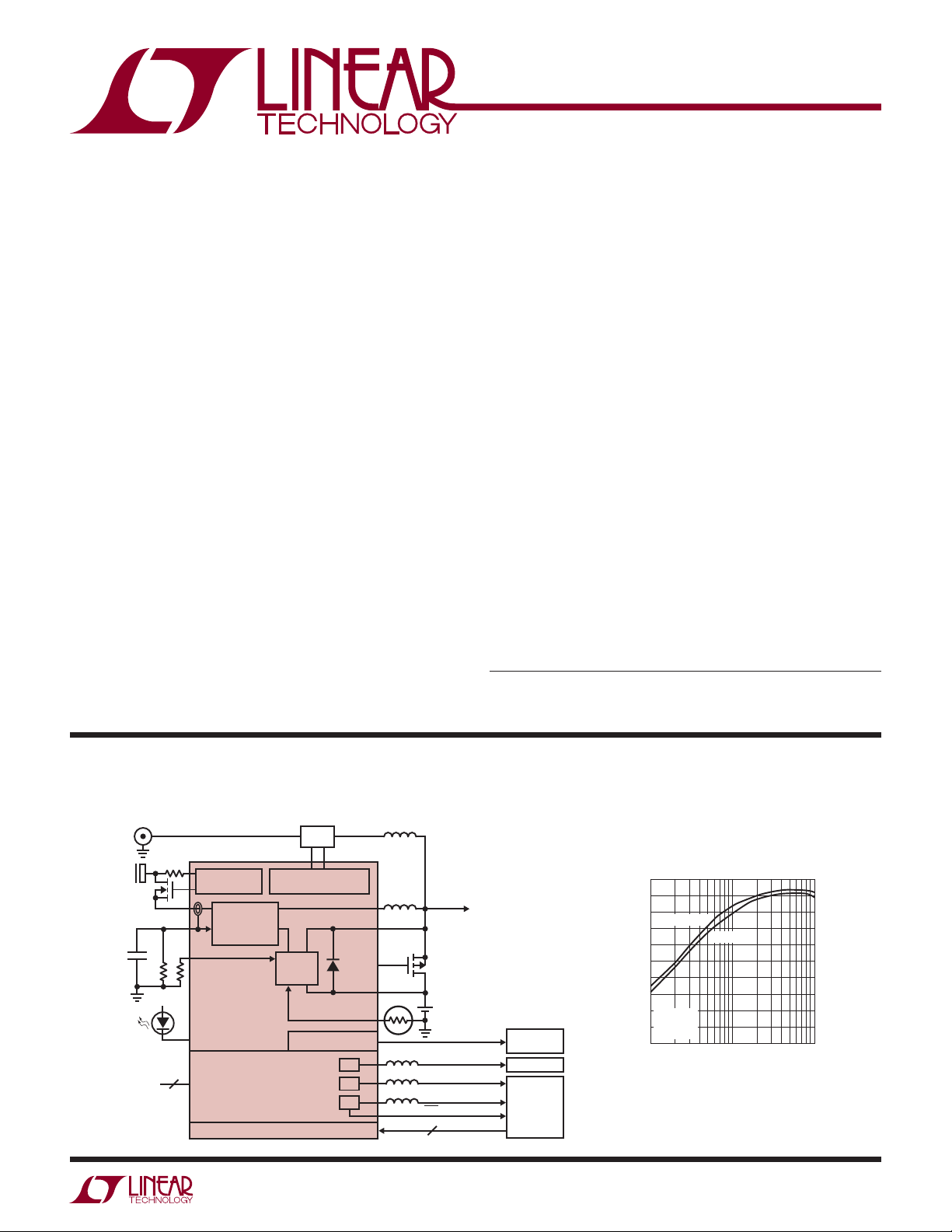
TYPICAL APPLICATION
High Effi ciency PowerPath Manager with Overvoltage Protection
and Triple Step-Down Regulator
AUTOMOTIVE
FIREWIRE, ETC.
USB OR
5V AC
ADAPTER
CONTROLS
ENABLE
CHARGE
6
OVERVOLTAGE
PROTECTION
USB COMPLIANT
BIDIRECTIONAL
SWITCHING
REGULATOR
LTC3576/LTC3576-1
HIGH EFFICIENCY
LT3653
EXTERNAL HIGH VOLTAGE
BUCK CONTROLLER
CC/CV
BATTERY
CHARGER
ALWAYS ON LDO
TRIPLE
STEP-DOWN
SWITCHING
REGULATORS
2
C PORT
I
0V
T
1
2
3
OPTIONAL
+
Li-Ion
3.3V/20mA
0.8V TO 3.6V/400mA
0.8V TO 3.6V/400mA
0.8V TO 3.6V/1A
RST
2
TO OTHER
LOADS
RTC/LOW
POWER LOGIC
MEMORY
I/O
CORE
µPROCESSOR
2
C
I
3576 TA01
PowerPath Switching Regulator Effi ciency
to System Load (P
100
90
80
BAT = 4.2V
70
60
50
40
EFFICIENCY (%)
30
20
V
BUS
I
BAT
10
10x MODE
0
10
= 5V
= 0mA
LOAD CURRENT (mA)
BAT = 3.3V
VOUT/PVBUS
100 1000
)
3576 TA01b
3576f
1
LTC3576/LTC3576-1
(Notes 1, 2, 3)
V
, WALL (Transient) t < 1ms,
BUS
Duty Cycle < 1% .......................................... –0.3V to 7V
, WALL (Static), BAT, V
V
BUS
, ENOTG, NTC, SDA, SCL, DVCC,
V
OUT
RST3, CHRG ................................................ –0.3V to 6V
, I
I
LIM0
.........–0.3V to Max(V
ILIM1
EN1, EN2, EN3 ...............................–0.3V to V
FBx (x = 1, 2, 3) ..............................–0.3V to V
I
OVSENS
I
CLPROG
I
CHRG
I
PROG
I
LDO3V3
I
SW1
I
SW
...................................................................10mA
....................................................................3mA
, I
............................................................50mA
RST3
........................................................................2mA
...................................................................30mA
, I
(Continuous) .......................................600mA
SW2
, I
, I
SW3
BAT
, I
(Continuous) ..............................2A
VOUT
Maximum Junction Temperature........................... 125°C
Operating Temperature Range.................. –40°C to 85°C
Storage Temperature Range ................... –65°C to 125°C
IN1
, V
IN2
BUS
, V
,
IN3
, V
, BAT) + 0.3V
OUT
OUT
INx
+ 0.3V
+ 0.3V
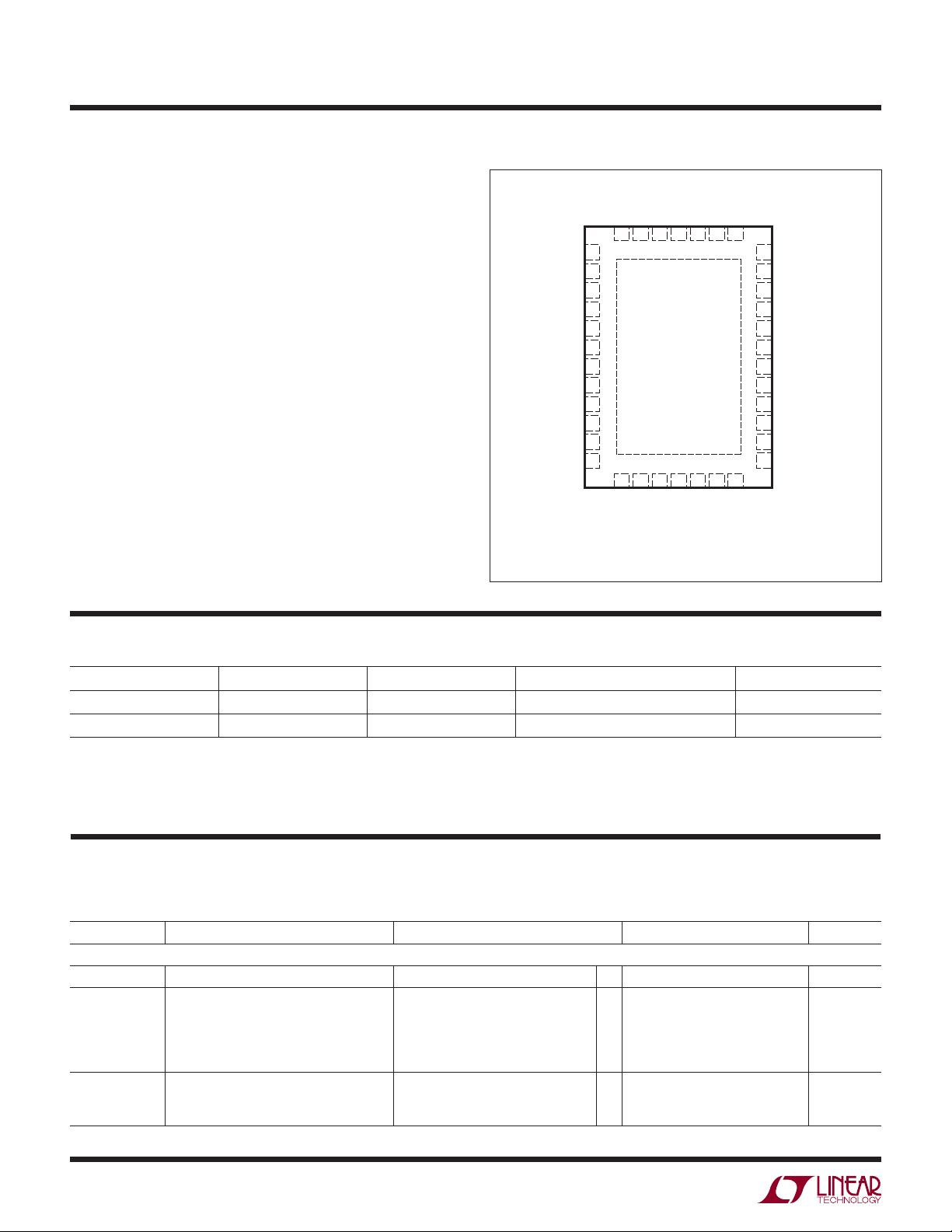
PIN CONFIGURATION ABSOLUTE MAXIMUM RATINGS
TOP VIEW
LIM1ILIM0
I
38 37 36 35 34 33 32
1CLPROG
LDO3V3
2
NTCBIAS
3
NTC
4
OVGATE
5
OVSENS
6
FB1
7
V
8
IN1
SW1
9
EN1
10
ENOTG
11
DV
12
CC
13 14 15 16
SCL
38-LEAD (4mm s 6mm) PLASTIC QFN
T
EXPOSED PAD (PIN 39) IS GND, MUST BE SOLDERED TO PCB
JMAX
BUSVBUSVOUT
SW
V
39
17 18 19
NC
SDA
UFE PACKAGE
= 125°C, θJA = 34°C/W
NC
IN3
V
SW3
BAT
EN3
31
30
29
28
27
26
25
24
23
22
21
20
IDGATE
CHRG
PROG
ACPR
WALL
V
C
FB2
V
IN2
SW2
EN2
RST3
FB3
ORDER INFORMATION
LEAD FREE FINISH TAPE AND REEL PART MARKING PACKAGE DESCRIPTION TEMPERATURE RANGE
LTC3576EUFE#PBF LTC3576EUFE#TRPBF 3576
LTC3576EUFE-1#PBF LTC3576EUFE-1#TRPBF 35761
Consult LTC Marketing for parts specifi ed with wider operating temperature ranges.
Consult LTC Marketing for information on non-standard lead based fi nish parts.
For more information on lead free part marking, go to: http://www.linear.com/leadfree/
For more information on tape and reel specifi cations, go to: http://www.linear.com/tapeandreel/
ELECTRICAL CHARACTERISTICS
The l denotes the specifi cations which apply over the full operating
temperature range, otherwise specifi cations are at TA = 25°C. V
BUS
38-Lead (4mm × 6mm) Plastic QFN
38-Lead (4mm × 6mm) Plastic QFN
= 5V, BAT = 3.8V, DVCC = 3.3V, R
CLPROG
otherwise noted.
SYMBOL PARAMETER CONDITIONS MIN TYP MAX UNITS
PowerPath Switching Regulator—Step-Down Mode
V
BUS
I
VBUS(LIM)
I
(Note 4) Input Quiescent Current
VBUSQ
Input Supply Voltage 4.35 5.5 V
Total Input Current
1× Mode
5× Mode
10× Mode
Low Power Suspend Mode
High Power Suspend Mode
1× Mode
5×, 10× Modes
Low/High Power Suspend Modes
l
82
l
440
l
800
l
0.32
l
1.6
–40°C to 85°C
–40°C to 85°C
= 3.01k, unless
90
472
880
0.39
2.05
7
17
0.045
100
500
1000
0.5
2.5
mA
mA
mA
mA
mA
mA
mA
mA
2
3576f

LTC3576/LTC3576-1
ELECTRICAL CHARACTERISTICS
The l denotes the specifi cations which apply over the full operating
temperature range, otherwise specifi cations are at T
= 25°C. V
A
otherwise noted.
SYMBOL PARAMETER CONDITIONS MIN TYP MAX UNITS
h
CLPROG
(Note 4)
I
VOUT(POWERPATH)VOUT
V
CLPROG
V
UVLO
V
DUVLO
V
V
OUT
f
OSC
R
PMOS_
POWERPATH
R
NMOS_
POWERPATH
I
PEAK_POWERPATH
R
SUSP
PowerPath Switching Regulator—Step-Up Mode (USB On-the-Go)
V
BUS
V
OUT
I
VBUS
I
PEAK
I
OTGQ
V
CLPROG
V
OUT(UVLO)
t
SCFAULT
Bat-Track Switching Regulator Control
V
WALL
ΔV
WALL
V
OUT
I
WALLQ
R
ACPR
V
HACPR
V
LACPR
Ratio of Measured V
CLPROG Program Current
Current to
BUS
1x Mode
5x Mode
10x Mode
Low Power Suspend Mode
High Power Suspend Mode
Current Available Before
Discharging Battery
1x Mode, BAT = 3.3V
5x Mode, BAT = 3.3V
10x Mode, BAT = 3.3V
Low Power Suspend Mode
High Power Suspend Mode
CLPROG Servo Voltage in Current Limit Switching Modes
Suspend Modes
V
Undervoltage Lockout Rising Threshold
BUS
Falling Threshold 3.95
V
to BAT Differential Undervoltage
BUS
Lockout
Voltage 1x, 5x, 10x Modes, 0V < BAT < 4.2V,
OUT
Rising Threshold
Falling Threshold
I
VOUT
USB Suspend Modes, I
Switching Frequency 1.8 2.25 2.7 MHz
PMOS On-Resistance 0.18
NMOS On-Resistance 0.30
Peak Inductor Current Limit 1x Mode (Note 5)
5x Mode (Note 5)
10x Mode (Note 5)
Suspend LDO Output Resistance Closed Loop 10
Output Voltage 0mA ≤ I
Input Voltage 2.9 5.5 V
Output Current Limit
V
Leakage Current in Shutdown On-the-Go Disabled, V
BUS
Peak Inductor Current Limit (Note 5) 1.8 A
V
Quiescent Current V
OUT
OUT
= 3.8V, I
Output Current Limit Servo Voltage 1.15 V
V
UVLO—V
OUT
V
UVLO—V
OUT
Short-Circuit Fault Delay V
OUT
OUT
Falling
Rising
< 4V and PMOS Switch Off 7.2 ms
BUS
Absolute WALL Input Threshold Rising Threshold
Hysteresis
Differential WALL Input Threshold WALL-BAT Falling
Hysteresis
Regulation Target Under VC Control 3.55 BAT + 0.3 V
WALL Quiescent Current 100 µA
ACPR Pull-Down Strength 100
ACPR High Voltage V
ACPR Low Voltage 0V
= 5V, BAT = 3.8V, DVCC = 3.3V, R
BUS
= 0mA, Battery Charger Off
= 250µA
VOUT
≤ 500mA, V
VBUS
VBUS
= 0mA (Note 6) 1.38 mA
> 3.2V 4.75 5.25 V
OUT
< UVLO
BUS
= 3.01k, unless
CLPROG
210
1160
2200
9.6
56
121
667
1217
0.26
1.6
0.31
2
0.41
2.4
1.18
100
4.30
4.35 V
4.00
200
50
3.4
4.5
BAT + 0.3
4.6
4.7
4.7
1
2
3
l
550
–150
680
0 150
2.5 2.6
2.8 2.9
4.2 4.3
4.4 V
1.1
0306045 mV
OUT
mA/mA
mA/mA
mA/mA
mA/mA
mA/mA
mA
mA
mA
mA
mA
mV
mV
mV
mA
nA
mV
3576f
V
V
V
V
A
A
A
V
V
V
V
3

LTC3576/LTC3576-1
ELECTRICAL CHARACTERISTICS
The l denotes the specifi cations which apply over the full operating
temperature range, otherwise specifi cations are at T
= 25°C. V
A
otherwise noted.
SYMBOL PARAMETER CONDITIONS MIN TYP MAX UNITS
Overvoltage Protection
V
OVCUTOFF
V
OVGATE
t
RISE
Battery Charger
V
FLOAT
I
CHG
I
BAT
V
PROG
V
PROG_TRKL
V
C/10
h
PROG
I
TRKL
V
TRKL
ΔV
TRKL
ΔV
RECHRG
t
TERM
t
BADBAT
h
C/10
V
CHRG
I
CHRG
R
ON_CHG
T
LIM
NTC
V
COLD
Overvoltage Protection Threshold With 6.2k Series Resistor 6.1 6.35 6.7 V
OVGATE Output Voltage V
OVSENS
V
OVSENS
OVGATE Time to Reach Regulation OVGATE C
BAT Regulated Output Voltage LTC3576
LTC3576-1
Constant Current Mode Charger Current R
Battery Drain Current V
PROG
R
PROG
BUS
I
VOUT
V
BUS
> V
= 0µA
= 0V, I
(Ideal Diode Mode)
PROG Pin Servo Voltage 1.000 V
PROG Pin Servo Voltage in Trickle Charge BAT < V
C/10 Threshold Voltage at PROG 100 mV
Ratio of I
to PROG Pin Current 1030 mA/mA
BAT
Trickle Charge Current BAT < V
Trickle Charge Threshold Voltage BAT Rising 2.7 2.85 3.0 V
Trickle Charge Hysteresis Voltage 135 mV
Recharge Battery Threshold Voltage Threshold Voltage Relative to V
Safety Timer Termination Period Timer Starts When V
Bad Battery Termination Time BAT < V
End of Charge Current Ratio (Note 7) 0.085 0.1 0.112 mA/mA
CHRG Pin Output Low Voltage I
CHRG Pin Leakage Current V
= 5mA 65 100 mV
CHRG
CHRG
Battery Charger Power FET OnResistance (Between V
and BAT)
OUT
Junction Temperature in Constant
Temperature Mode
Cold Temperature Fault Threshold Voltage Rising Threshold
Hysteresis
= 5V, BAT = 3.8V, DVCC = 3.3V, R
BUS
< V
OVCUTOFF
> V
OVCUTOFF
= 1nF 1.25 ms
LOAD
4.179
l
4.165
4.079
l
4.065
= 1k
= 5k
, Suspend Mode,
UVLO
VOUT
TRKL
, R
TRKL
PROG
TRKL
= 0µA
= 1k 100 mA
FLOAT
= V
BAT
FLOAT
980
185
–75 –100 –125 mV
3.3 4 5 Hour
0.4 0.5 0.6 Hour
= 3.01k, unless
CLPROG
1.88•V
OVSENS
12 V
0
4.200
4.200
4.100
4.100
1030
206
4.221
4.235
4.121
4.135
1065
223
3.6 6 µA
28 45 µA
0.100 V
mA
mA
= 5V 1 µA
0.18
110 °C
75 76.5
1.5
78 %NTCBIAS
%NTCBIAS
V
V
V
V
V
V
HOT
V
DIS
I
NTC
Ideal Diode
V
FWD
R
DROPOUT
I
MAX_DIODE
4
Hot Temperature Fault Threshold Voltage Falling Threshold
Hysteresis
NTC Disable Threshold Voltage Falling Threshold
Hysteresis
33.4 34.9
1.5
0.7 1.7
50
36.4 %NTCBIAS
%NTCBIAS
2.7 %NTCBIAS
mV
NTC Leakage Current NTC = NTCBIAS = 5V –50 50 nA
Forward Voltage I
Internal Diode On-Resistance Dropout I
= 10mA 15 mV
VOUT
= 200mA 0.18
VOUT
Diode Current Limit 2 A
3576f
LTC3576/LTC3576-1
ELECTRICAL CHARACTERISTICS
The l denotes the specifi cations which apply over the full operating
temperature range, otherwise specifi cations are at T
= 25°C. V
A
otherwise noted.
SYMBOL PARAMETER CONDITIONS MIN TYP MAX UNITS
Always On 3.3V LDO Supply
V
LDO3V3
R
CL_LDO3V3
R
OL_LDO3V3
Logic (I
LIM0
V
IL
V
IH
I
PD1
2
C Port
I
DV
CC
I
DVCC
V
DVCC(UVLO)
ADDRESS I
V
, SDA, SCL Input High Threshold 70 %DV
IH
VIL, SDA, SCL Input Low Threshold 30 %DV
I
, SDA, SCL Pull-Down Current 2µA
PD2
V
OL
f
SCL
t
BUF
t
HD_STA
t
SU_STA
t
SU_STO
t
HD_DAT(O)
t
HD_DAT(I)
t
SU_DAT
t
LOW
t
HIGH
t
f
t
r
t
SP
General Purpose Switching Regulators 1, 2 and 3
V
IN1,2,3
V
OUT(UVLO)
f
OSC
I
FB1,2,3
D1,2,3 Maximum Duty Cycle 100 %
R
SW1,2,3_PD
Regulated Output Voltage 0mA < I
Closed-Loop Output Resistance 2.7
Dropout Output Resistance 23
, I
, EN1, EN2, EN3, ENOTG, and SCL, SDA when DVCC = 0V)
LIM1
Logic Low Input Voltage 0.4 V
Logic High Input Voltage 1.2 V
I
, I
LIM0
, EN1, EN2, EN3, ENOTG, SCL,
LIM1
SDA Pull-Down Current
Input Supply 1.6 5.5 V
DVCC Current SCL/SDA = 0kHz, DVCC = 3.3V 0.5 µA
DVCC UVLO 1.0 V
2
C Address 0001001[0]
Digital Output Low (SDA) I
= 3mA 0.4 V
SDA
Clock Operating Frequency 400 kHz
Bus Free Time Between Stop and Start
Condition
Hold Time After (Repeated) Start
Condition
Repeated Start Condition Setup Time 0.6 µs
Stop Condition Setup Time 0.6 µs
Data Hold Time Output 0 900 ns
Data Hold Time Input 0 ns
Data Setup Time 100 ns
SCL Low Period 1.3 µs
SCL High Period 0.6 µs
SDA/SCL Fall Time 20 300 ns
SDA/SCL Rise Time 20 300 ns
Input Spike Suppression Pulse Width 50 ns
Input Supply Voltage (Note 8) 2.7 5.5 V
V
OUT
V
OUT
UVLO—V
UVLO—V
OUT
OUT
Falling
Rising
V
IN1,2,3
Low Impedance. Switching
Regulators are Disabled in UVLO
Switching Frequency 1.8 2.25 2.7 MHz
FBx Input Current V
FB1,2,3
SWx Pull-Down in Shutdown 10 k
= 5V, BAT = 3.8V, DVCC = 3.3V, R
BUS
< 20mA 3.1 3.3 3.5 V
LDO3V3
= 3.01k, unless
CLPROG
2µA
1.3 µs
0.6 µs
Connected to V
Through
OUT
2.5 2.6
2.8 2.9
= 0.85V –50 50 nA
CC
CC
V
V
3576f
5
LTC3576/LTC3576-1
ELECTRICAL CHARACTERISTICS
The l denotes the specifi cations which apply over the full operating
temperature range, otherwise specifi cations are at T
= 25°C. V
A
otherwise noted.
SYMBOL PARAMETER CONDITIONS MIN TYP MAX UNITS
I
VIN1,2,3
V
FBHIGH1,2,3
V
FBLOW1,2,3
V
LSB1,2,3
R
LDO_CL1,2,3
R
LDO_OL1,2,3
General Purpose Switching Regulator 1 and 2
I
LIM1,2
I
OUT1,2
R
P1,2
R
N1,2
General Purpose Switching Regulator 3
I
LIM3
I
OUT3
R
P3
R
N3
t
RST3
Burst Mode is a registered trademark of Linear Technology Corporation.
Pulse Skip Mode Input Current I
Burst Mode
®
Input Current I
LDO Mode Input Current I
Shutdown Input Current Limit I
OUT1,2,3
OUT1,2,3
OUT1,2,3
OUT1,2,3
Maximum Servo Voltage Full Scale (1,1,1,1) (Note 10)
Minimum Servo Voltage Zero Scale (0,0,0,0) (Note 10) 0.405 0.425 0.445 V
V
Servo Voltage Step Size 25 mV
FB1,2
LDO Mode Closed-Loop R
LDO Mode Open-Loop R
OUT
OUT
V
FB1,2,3
(Note 11) 2.5
PMOS Switch Current Limit Pulse Skip/Burst Mode Operation
(Note 5)
Available Output Current LDO Mode 50 mA
PMOS R
DS(ON)
NMOS R
DS(ON)
PMOS Switch Current Limit Pulse Skip/Burst Mode Operation
(Note 5)
Available Output Current LDO Mode 50 mA
PMOS R
DS(0N)
NMOS R
DS(ON)
Power-On Reset Time for Switching
Regulator
V
Within 92% of Final Value to
FB3
RST3 Hi-Z
= 5V, BAT = 3.8V, DVCC = 3.3V, R
BUS
= 3.01k, unless
CLPROG
= 0µA (Note 9) 90 µA
= 0µA (Note 9) 20 35 µA
= 0µA (Note 9) 15 25 µA
= 0µA, FB1,2,3 = 0V 1 µA
l
0.78 0.80 0.82 V
= V
= 0.8V 0.25
OUT1,2 3
600 900 1300 mA
0.6
0.7
1300 1800 2800 mA
0.18
0.3
230 ms
Note 1: Stresses beyond those listed under Absolute Maximum Ratings
may cause permanent damage to the device. Exposure to any Absolute
Maximum Rating condition for extended periods may affect device
reliability and lifetime.
Note 2: The LTC3576E/LTC3576E-1 are guaranteed to meet performance
specifi cations from 0°C to 85°C. Specifi cations over the –40°C to 85°C
operating temperature range are assured by design, characterization and
correlation with statistical process controls.
Note 3: The LTC3576E/LTC3576E-1 include overtemperature protection
that is intended to protect the device during momentary overload
conditions. Junction temperature will exceed 125°C when overtemperature
protection is active. Continuous operation above the specifi ed maximum
operating junction temperature may impair device reliability.
Note 4: Total input current is the sum of quiescent current, I
measured current given by V
CLPROG
/R
CLPROG
• (h
CLPROG
VBUSQ
+ 1).
, and
Note 5: The current limit features of this part are intended to protect the
IC from short term or intermittent fault conditions. Continuous operation
above the maximum specifi ed pin current rating may result in device
degradation or failure.
Note 6: The bidirectional switcher’s supply current is bootstrapped to V
and in the application will refl ect back to V
OUT
by (V
BUS/VOUT
) •
BUS
1/effi ciency. Total quiescent current is the sum of the current into the
V
pin plus the refl ected current.
OUT
Note 7: h
is expressed as a fraction of the measured full charge
C/10
current with indicated PROG resistor.
Note 8: V
not in UVLO.
OUT
Note 9: FBx above regulation such that regulator is in sleep. Specifi cation
does not include resistive divider current refl ected back to V
INx
.
Note 10: Applies to pulse skip and Burst Mode operation only.
Note 11: Inductor series resistance adds to open-loop R
OUT
.
3576f
6
LTC3576/LTC3576-1
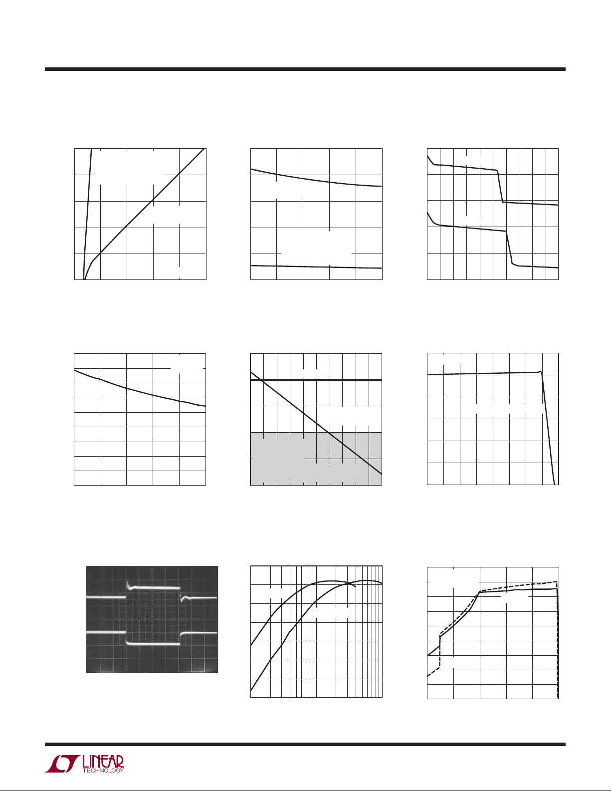
TYPICAL PERFORMANCE CHARACTERISTICS
Ideal Diode Resistance
Ideal Diode V-I Characteristics
1.0
0.8
0.6
0.4
CURRENT (A)
0.2
INTERNAL IDEAL DIODE
WITH SUPPLEMENTAL
EXTERNAL VISHAY
Si2333 PMOS
0
0.04
0
INTERNAL IDEAL
DIODE ONLY
0.12
0.08
FORWARD VOLTAGE (V)
V
0.16
BUS
USB Limited Load Current vs Battery
Voltage (Battery Charger Disabled)
900
800
700
600
500
400
300
LOAD CURRENT (mA)
200
100
0
2.7
3.0 3.6
BATTERY VOLTAGE (V)
3.3
V
BUS
5x MODE
3.9
= 5V
0.20
3576 G01
= 5V
4.2
3576 G04
vs Battery Voltage
0.25
0.20
INTERNAL IDEAL
0.15
0.10
RESISTANCE ()
0.05
0
3.0
2.7
Battery and V
vs Load Current
750
500
250
0
CURRENT (mA)
V
= 5V
BUS
BAT = 3.8V
–250
5x MODE
R
CLPROG
= 1k
R
PROG
–500
100 200 300
0
DIODE
INTERNAL IDEAL DIODE
WITH SUPPLEMENTAL
EXTERNAL VISHAY
Si2333 PMOS
3.6
3.3
BATTERY VOLTAGE (V)
Currents
BUS
V
CURRENT
BUS
BATTERY CURRENT
(CHARGING)
= 3.01k
BATTERY CURRENT
(DISCHARGING)
600 700 900
400 500
LOAD CURRENT (mA)
TA = 25°C unless otherwise specifi ed.
Voltage vs Load Current
V
OUT
(Battery Charger Disabled)
4.50
BAT = 4V
4.25
4.00
(V)
3.9
3576 G02
4.2
OUT
V
3.75
3.50
3.25
0
BAT = 3.4V
0.1 0.2 0.3
0.4 0.5
LOAD CURRENT (A)
Battery Charge Current vs
Temperature
600
R
= 2k
PROG
500
400
THERMAL REGULATION
040
TEMPERATURE (°C)
800
3576 G05
1000
300
200
CHARGE CURRENT (mA)
100
0
–40
–20 20
0.6 0.7 0.9
0.8
80
60
100
1.0
3576 G03
120
3576 G06
V
OUT
50mV/DIV
AC COUPLED
I
VOUT
500mA/DIV
0mA
PowerPath Switching Regulator
Transient Response
V
= 5V
BUS
= 3.65V
V
OUT
CHARGER OFF
10x MODE
20µs/DIV
3576 G07
PowerPath Switching Regulator
Effi ciency vs Load Current
100
90
1x MODE
80
70
60
EFFICIENCY (%)
50
40
30
10
5x, 10x MODE
100
LOAD CURRENT (mA)
3576 G08
1000
Battery Charging Effi ciency vs
Battery Voltage with No External
Load (P
95
R
CLPROG
R
90
PROG
85
80
75
70
EFFICIENCY (%)
65
5x MODE
60
55
50
2.7
BAT/PVBUS
= 3.01k
= 1k
3.0 3.6
BATTERY VOLTAGE (V)
)
1x MODE
3.3
3.9
4.2
3576 G09
3576f
7
LTC3576/LTC3576-1
TYPICAL PERFORMANCE CHARACTERISTICS
V
Quiescent Current vs
BUS
V
Voltage (Suspend)
BUS
60
50
40
30
20
QUIESCENT CURRENT (µA)
10
0
0
1234
BUS VOLTAGE (V)
Battery Charge Current vs V
Voltage
600
R
= 3.01k
CLPROG
= 2k
R
PROG
500
5x MODE
400
300
200
BATTERY CURRENT (mA)
100
0
3.40
3.50 3.60
3.45 3.55
V
(V)
OUT
3.65
3.70
OUT
3.75
3576 G10
3576 G13
3.80
(V)
OUT
V
3.0
5
4.7
4.5
4.3
4.1
3.9
(V)
3.7
OUT
V
3.5
3.3
3.1
2.9
2.7
Voltage vs Load Current in
V
OUT
Suspend
5.0
4.5
3.5
2.5
4.0
0
V
HIGH POWER SUSPEND
LOW POWER SUSPEND
V
= 5V
BUS
BAT = 3.3V
= 3.01k
R
CLPROG
0.5
LOAD CURRENT (mA)
Voltage vs Battery Voltage
OUT
1.0
1.5
(Charger Overprogrammed)
V
= 5V
BUS
= 0V
I
VOUT
= 3.01k
R
CLPROG
= 1k
R
PROG
5x MODE
1x MODE
2.7
3.0
BATTERY VOLTAGE (V)
3.3
3.6
TA = 25°C unless otherwise specifi ed.
V
Current vs Load Current in
BUS
Suspend
2.5
V
= 5V
BUS
BAT = 3.3V
= 3.01k
R
CLPROG
2.0
1.5
HIGH POWER
SUSPEND
LOW POWER SUSPEND
0.5
0
1.0
LOAD CURRENT (mA)
2.0
3576 G11
2.5
CURRENT (mA)
1.0
BUS
V
0.5
0
Normalized Battery Charger Float
Voltage vs Temperature
1.001
1.000
0.999
0.998
0.997
NORMALIZED FLOAT VOLTAGE
3.9
3576 G14
4.2
0.996
–40
–15
10
TEMPERATURE (°C)
1.5
35
2.0
2.5
3576 G12
60
85
3576 G15
V
Quiescent Current vs
BUS
Temperature
25
V
= 5V
BUS
20
15
10
QUIESCENT CURRENT (mA)
5
0
–15
–40
8
5x MODE
1x MODE
35
10
TEMPERATURE (°C)
V
Quiescent Current in
BUS
Suspend vs Temperature
60
V
= 5V
BUS
50
40
30
20
QUIESCENT CURRENT (µA)
10
0
–40
60
85
3576 G16
–15 10 35 60
TEMPERATURE (°C)
85
3576 G17
Battery Drain Current vs
Temperature
35
30
25
20
15
10
BATTERY CURRENT (µA)
5
0
–15 10 35 85
–40
TEMPERATURE (°C)
BAT = 3.8V
= 0V
V
BUS
SWITCHING
REGULATORS OFF
60
3576 G18
3576f
LTC3576/LTC3576-1
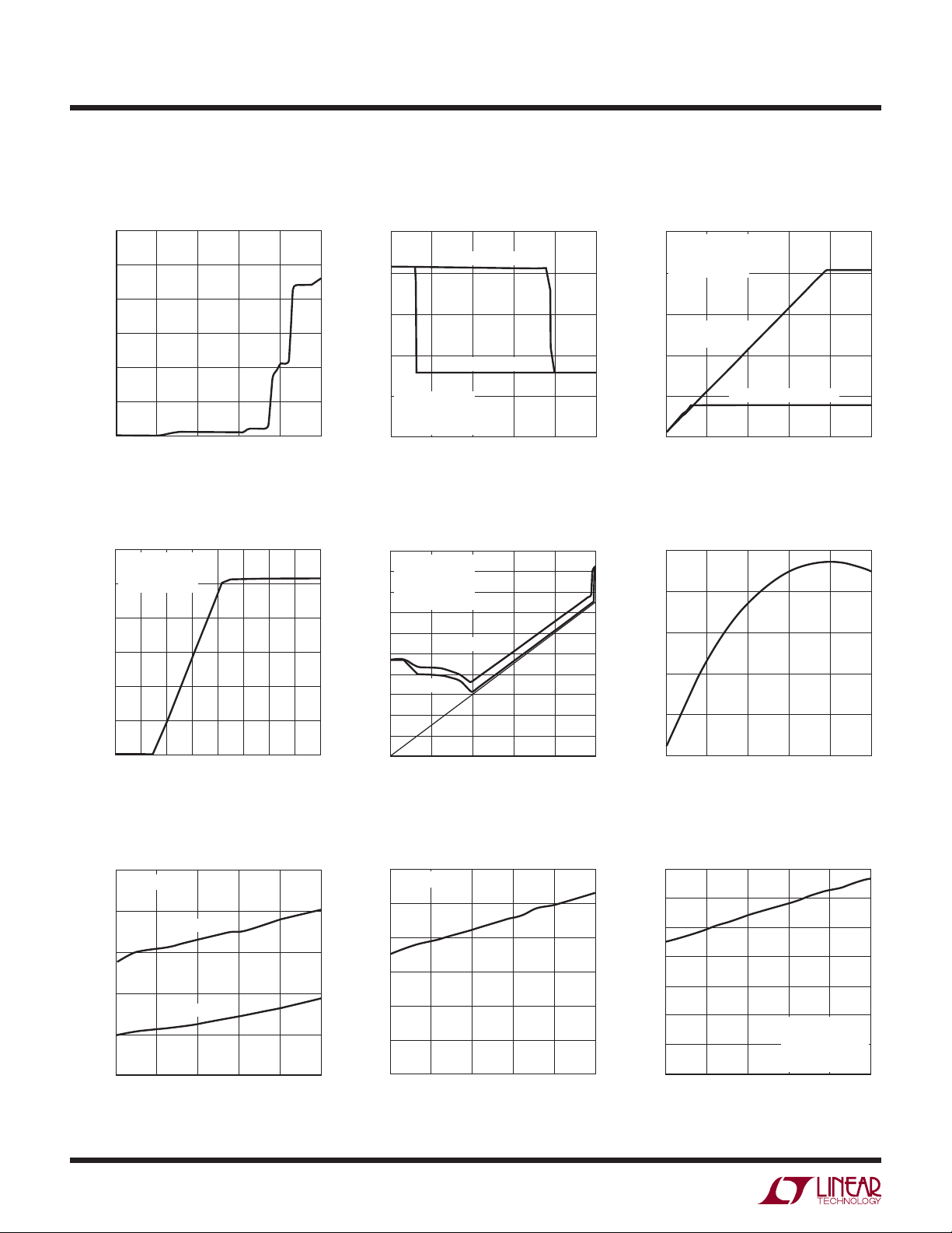
TYPICAL PERFORMANCE CHARACTERISTICS
OTG Boost Quiescent Current
vs V
Voltage
OUT
2.5
2.3
2.1
1.9
1.7
1.5
1.3
1.1
QUIESCENT CURRENT (mA)
0.9
0.7
0.5
2.90
3.55
4.20
V
(V)
OUT
OTG Boost Effi ciency
vs V
Voltage
OUT
95
500mA LOAD
90
85
80
EFFICIENCY (%)
75
100mA LOAD
4.85
3576 G19
5.50
OTG Boost V
vs Load Current
5.5
5.0
0 100
V
V
OUT
V
OUT
V
OUT
V
OUT
(V)
BUS
V
4.5
4.0
3.5
3.0
OTG Boost Start-Up Time into
Current Source Load vs V
Voltage
2.50
2.25
2.00
TIME (ms)
1.75
22µF ON V
22µF ON V
LOAD THROUGH OVP
Voltage
BUS
= 4.75V
BUS
I
= 500mA
VBUS
= 5V
= 4.4V
= 3.8V
= 3.2V
400
300
200
LOAD CURRENT (mA)
, 22µF AND
BUS
LOAD THROUGH OVP
22µF ON V
,
BUS
500
OUT
NO OVP
TA = 25°C unless otherwise specifi ed.
OTG Boost Effi ciency
vs Load Current
100
90
80
70
EFFICIENCY (%)
60
50
600
700
3576 G20
40
1
10 100 1000
LOAD CURRENT (mA)
OTG Boost Burst Mode Current
BUS
Threshold vs V
400
300
,
200
LOAD CURRENT (mA)
100
FALLING THRESHOLD
OUT
RISING THRESHOLD
Voltage
V
= 5V
OUT
= 4.4V
V
OUT
= 3.8V
V
OUT
= 3.2V
V
OUT
3576 G21
70
2.90
V
BUS
50mV/DIV
AC COUPLED
I
VBUS
200mA/DIV
0mA
3.55
1.50
2.9
4.20
V
OUT
(V)
4.85
5.50
3576 G22
3.4 3.9 4.4 4.9
V
(V)
OUT
5.4
3576 G23
0
2.90
3.55
V
4.20
OUT
(V)
4.85
5.50
3576 G24
OTG Boost Start-Up into Current
Source Load
50mV/DIV
I
VBUS
200mA/DIV
0mA
V
BUS
2V/DIV
0V
V
= 3.8V
OUT
20µs/DIV
3576 G25
V
I
LOAD
OUT
= 3.8V
= 500mA
200µs/DIV
AC COUPLED
3576 G26
V
BUS
V
1V/DIV
SW
OTG Boost Burst Mode OperationOTG Boost Transient Response
0V
OUT
I
LOAD
= 3.8V
= 10mA
50µs/DIVV
3576 G27
3576f
9
LTC3576/LTC3576-1
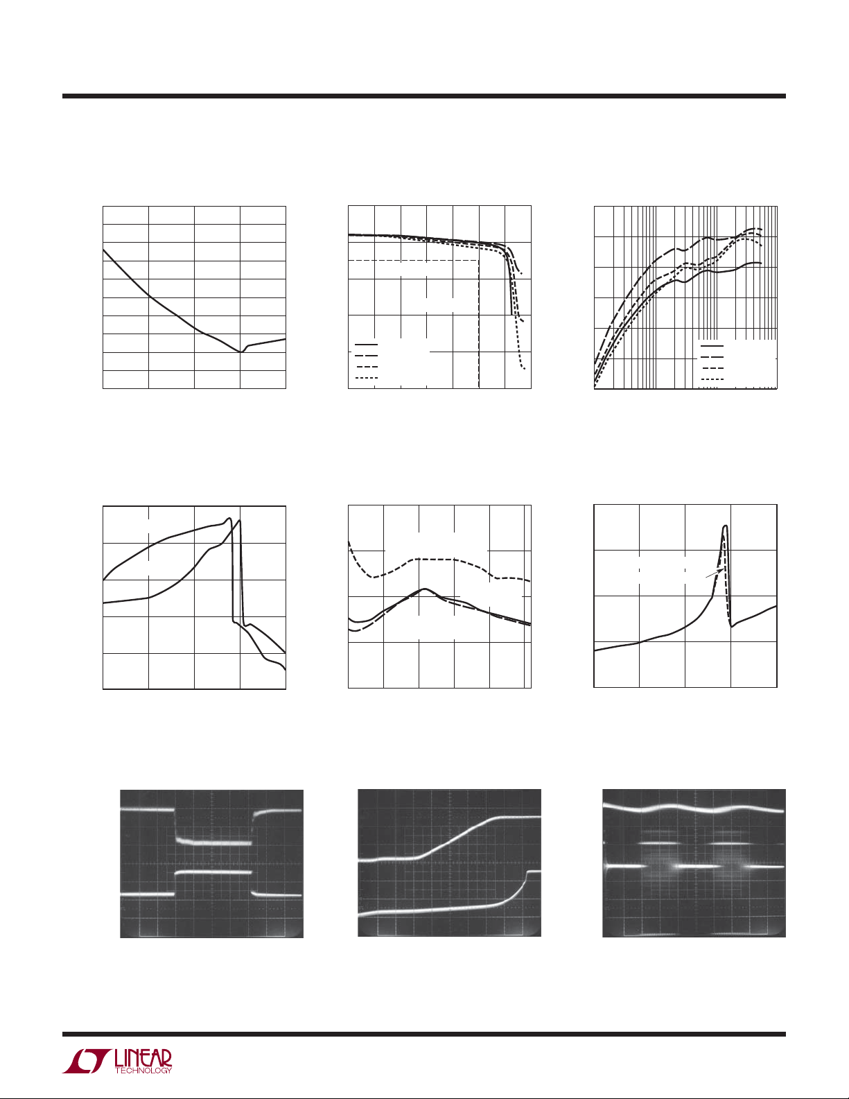
TYPICAL PERFORMANCE CHARACTERISTICS
Battery Charging from USB-HV
USB OTG from BAT-HV BUCK-BAT
V
OUT
1V/DIV
V
BUS
I
BAT
0A
HVOK
5V/DIV
0V
V
V
BUS
5V/DIV
= 3.8V
BAT
= 285mA
I
BUS
= 12V
HV
IN
USING LT3653
500µs/DIV
V
OUT
1V/DIV
AC COUPLED
V
BUS
100mV/DIV
AC COUPLED
V
5V/DIV
HVOK
5V/DIV
V
BUS
5V/DIV
BUCK-USB
AC COUPLED
200mV/DIV
SW
0V
0V
V
BUS
HV
USING LT3653
IN
= 5V
= 12V
500µs/DIV
AC COUPLED
1A/DIV
3576 G28
OVP Connect Waveform OVP Disconnect Waveform
TA = 25°C unless otherwise specifi ed.
Oscillator Frequency vs
Temperature
2.30
2.25
2.20
2.15
FREQUENCY (MHz)
3576 G29
2.10
2.05
–40
–15
10
TEMPERATURE (°C)
Rising OVP Threshold vs
Temperature
6.280
6.275
V
= 5V
OUT
= 4.2V
V
OUT
= 3.6V
V
OUT
= 3V
V
OUT
= 2.7V
V
OUT
35
60
85
3576 G30
OVGATE
5V/DIV
OVP INPUT
VOLTAGE
0V TO 5V
STEP 5V/DIV
OVGATE vs OVSENS
12
OVSENS CONNECTED
TO INPUT THROUGH
6.2k RESISTOR
10
8
6
OVGATE (V)
4
2
0
0
OVP INPUT
STEP 5V/DIV
500µs/DIV
24 68
INPUT VOLTAGE (V)
3576 G31
3576 G34
OVGATE
5V/DIV
VOLTAGE
5V TO 10V
500µs/DIV
OVGATE Quiescent Current vs
Temperature
37
V
= 5V
OVSENS
35
33
31
QUIESCENT CURRENT (µA)
29
27
–40
–15
10
TEMPERATURE (°C)
6.270
6.265
OVP THRESHOLD (V)
3576 G32
6.260
6.255
–40
–15
10
TEMPERATURE (°C)
35
60
85
3576 G33
RST3, CHRG Pin Current vs
Voltage (Pull-Down State)
100
V
= 5V
BUS
BAT = 3.8V
80
60
40
20
RST3, CHRG PIN CURRENT (mA)
35
60
85
3576 G35
0
1
0
RST3, CHRG PIN VOLTAGE (V)
3
4
2
5
3576 G36
10
3576f
LTC3576/LTC3576-1
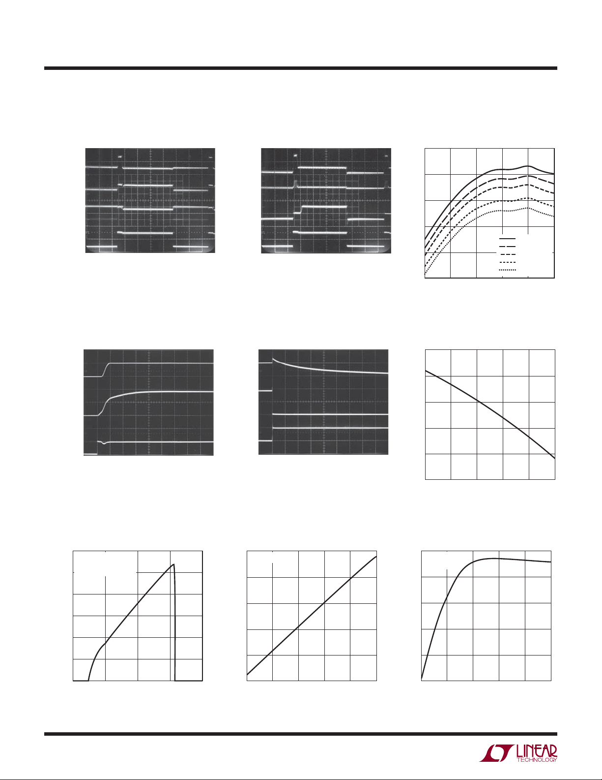
TYPICAL PERFORMANCE CHARACTERISTICS
3.3V LDO Output Voltage vs
Load Current, V
3.4
BAT = 3.9V, 4.2V
3.2
3.0
OUTPUT VOLTAGE (V)
BAT = 3V
2.8
BAT = 3.1V
BAT = 3.2V
BAT = 3.3V
2.6
5
0
LOAD CURRENT (mA)
10
= 0V
BUS
BAT = 3.4V
15
Switching Regulator Soft-Start
Waveform
500mV/DIV
OUT
V
50µs/DIV
BAT = 3.5V
BAT = 3.6V
20
3576 G37
3576 G40
20mV/DIV
AC COUPLED
25
3.3V LDO Step Response
(5mA to 15mA)
I
LDO3V3
5mA/DIV
0mA
V
LDO3V3
20µs/DIVBAT = 3.8V
Switching Regulator Current Limit
vs Temperature
2.0
REGULATOR 3
1.5
1.0
CURRENT LIMIT (A)
0.5
V
IN1,2,3
0
–40
REGULATORS 1, 2
= 3.8V
–15
10
TEMPERATURE (°C)
35
TA = 25°C unless otherwise specifi ed.
Battery Drain Current vs
Battery Voltage
35
I
= 0mA
VOUT
30
V
= 0V
BUS
25
20
15
10
3576 G38
BATTERY CURRENT (µA)
5
0
2.7
R
DS(ON)
V
BUS
(SUSPEND MODE)
3.0 3.3 3.6 4.2
BATTERY VOLTAGE (V)
for Switching Regulator
Power Switches vs Temperature
1.0
0.8
NMOS SWITCH
0.6
PMOS SWITCH
0.4
ON-RESISTANCE (Ω)
NMOS SWITCH
0.2
PMOS SWITCH
0
–15
60
85
3576 G41
–40
10
TEMPERATURE (°C)
= 5V
3.9
REGULATORS 1, 2
REGULATOR 3
35
60
3576 G39
85
3576 G42
Switching Regulator Low Power
Quiescent Currents vs Temperature
100
90
80
70
60
50
40
30
QUIESCENT CURRENTS (μA)
20
10
0
–40
PULSE-SKIP MODE
Burst Mode OPERATION
LDO MODE
–15
10
TEMPERATURE (°C)
35
Switching Regulators 1, 2
Pulse-Skip Mode Effi ciency
100
V
= 3.8V
IN3
90
80
70
60
50
40
EFFICIENCY (%)
30
20
10
0
60
85
3576 G43
0.1 10 100 1000
V
= 2.5V
OUT1,2
V
OUT1,2
V
= 1.8V
OUT1,2
1
LOAD CURRENT (mA)
= 1.2V
3576 G44
Switching Regulators 1, 2
Burst Mode Effi ciency
100
V
IN3
90
80
70
60
50
40
EFFICIENCY (%)
30
20
10
0
0.1 10 100 1000
V
= 3.8V
OUT1,2
V
OUT1,2
1
LOAD CURRENT (mA)
= 2.5V
V
OUT1,2
= 1.8V
= 1.2V
3576 G45
3576f
11
LTC3576/LTC3576-1
TYPICAL PERFORMANCE CHARACTERISTICS
Switching Regulator Constant
Frequency Quiescent Currents
8
7
6
5
4
3
2
QUIESCENT CURRENT (mA)
1
0
–40
SWITCHING
REGULATOR 3
SWITCHING
REGULATORS 1, 2
–15 10 60
TEMPERATURE (°C)
35
Switching Regulators 1, 2
Feedback Voltage vs Load Current
0.820
0.815
0.810
0.805
0.800
FEEDBACK VOLTAGE (V)
0.795
0.790
0.1 10 100 1000
Burst Mode
OPERATION
PULSE-SKIP
MODE
1
LOAD CURRENT (mA)
Switching Regulator 3 Feedback
Voltage vs Load Current
0.810
85
3576 G46
50mV/DIV
AC COUPLED
200mA/DIV
3576 G49
Switching Regulator 3
Pulse-Skip Mode Effi ciency
100
V
= 3.8V
IN3
90
80
70
60
50
40
EFFICIENCY (%)
30
20
10
0
0.1 10 100 1000
V
= 2.5V
OUT3
V
OUT3
V
= 1.2V
OUT3
1
LOAD CURRENT (mA)
= 1.8V
Switching Regulators 1, 2
Transient Response
V
OUT2
I
OUT2
0mA
V
V
IN2
OUT2
= 3.8V
= 3.4V
50µs/DIV
Switching Regulator 3
Transient Response
TA = 25°C unless otherwise specifi ed.
Switching Regulator 3
Burst Mode Effi ciency
100
V
3576 G47
= 3.8V
IN3
90
80
70
60
50
40
EFFICIENCY (%)
30
20
10
0
0.1 10 100 1000
V
OUT3
V
= 1.2V
OUT3
V
= 1.8V
OUT3
1
LOAD CURRENT (mA)
Switching Regulator Mode
Transition, Pulse Skip-LDOPulse Skip
V
OUT3
50mV/DIV
AC COUPLED
V
SW3
1V/DIV
0V
3576 G50
V
V
I
OUT3
IN3
OUT3
= 3.8V
= 1.8V
= 50mA
50µs/DIV
Switching Regulator Mode
Transition, Pulse Skip–Burst
Mode Operation–Pulse Skip
= 2.5V
3576 G48
3576 G51
0.805
0.800
FEEDBACK VOLTAGE (V)
0.795
0.790
0.1 10 100 1000
Burst Mode
OPERATION
PULSE SKIP MODE
1
LOAD CURRENT (mA)
12
3576 G52
V
OUT3
50mV/DIV
AC COUPLED
I
OUT3
500mA/DIV
0mA
V
V
IN3
OUT3
= 3.8V
= 1.8V
50µs/DIV
3576 G53
V
OUT3
50mV/DIV
AC COUPLED
V
SW3
1V/DIV
0V
V
IN3
V
OUT3
I
OUT3
= 3.8V
= 1.8V
= 100mA
50µs/DIV
3576 G54
3576f

PIN FUNCTIONS
LTC3576/LTC3576-1
CLPROG (Pin 1): USB Current Limit Program and Monitor
Pin. A 1% resistor from CLPROG to ground determines
the upper limit of the current drawn or sourced from the
pins. A precise fraction, h
V
BUS
CLPROG
, of the V
BUS
current is sent to the CLPROG pin when the PMOS switch of
the PowerPath switching regulator is on. The switching
regulator delivers power until the CLPROG pin reaches
1.18V in step-down mode and 1.15V in step-up mode.
When the switching regulator is in step-down mode,
CLPROG is used to regulate the average input current.
Several V
current limit settings are available via user
BUS
input which will typically correspond to the 500mA and
100mA USB specifi cations. When the switching regulator
is in step-up mode (USB on-the-go), CLPROG is used to
limit the average output current to 680mA. A multilayer
ceramic averaging capacitor or R-C network is required
at CLPROG for fi ltering.
LDO3V3 (Pin 2): 3.3V LDO Output Pin. This pin provides
a regulated always-on 3.3V supply voltage. LDO3V3
gets its power from V
. It may be used for light loads
OUT
such as a watchdog microprocessor or real time clock.
A 1µF capacitor is required from LDO3V3 to ground. If
the LDO3V3 output is not used it should be disabled by
connecting it to V
OUT
.
NTCBIAS (Pin 3): NTC Thermistor Bias Output. If NTC
operation is desired, connect a bias resistor between
NTCBIAS and NTC, and an NTC thermistor between NTC
and GND. To disable NTC operation, connect NTC to GND
and leave NTCBIAS open.
NTC (Pin 4): Input to the Thermistor Monitoring Circuits.
The NTC pin connects to a negative temperature coeffi cient
thermistor, which is typically co-packaged with the battery,
to determine if the battery is too hot or too cold to charge.
If the battery’s temperature is out of range, charging is
paused until it re-enters the valid range. A low drift bias
resistor is required from NTCBIAS to NTC and a thermistor
is required from NTC to ground. To disable NTC operation,
connect NTC to GND and leave NTCBIAS open.
OVGATE (Pin 5): Overvoltage Protection Gate Output.
Connect OVGATE to the gate pin of an external N-channel
MOS pass transistor. The source of the transistor should
be connected to V
and the drain should be connected
BUS
to the product’s DC input connector. In the absence of an
overvoltage condition, this pin is connected to an internal
charge pump capable of creating suffi cient overdrive to fully
enhance the pass transistor. If an overvoltage condition is
detected, OVGATE is brought rapidly to GND to prevent
damage to the LTC3576/LTC3576-1. OVGATE works in
conjunction with OVSENS to provide this protection.
OVSENS (Pin 6): Overvoltage Protection Sense Input.
OVSENS should be connected through a 6.2k resistor to
the input power connector and the drain of an external
N-channel MOS pass transistor. When the voltage on this
pin exceeds
V
OVCUTOFF
,
the OVGATE pin will be pulled
to GND to disable the pass transistor and protect the
LTC3576/LTC3576-1. The OVSENS pin shunts current
during an overvoltage transient in order to keep the pin
voltage at 6V.
FB1 (Pin 7): Feedback Input for Switching Regulator 1.
When regulator 1’s control loop is complete, this pin servos
to 1 of 16 possible set points based on the commanded
2
value from the I
(Pin 8): Power Input for Switching Regulator 1.
V
IN1
This pin will generally be connected to V
C serial port. See Table 4.
OUT
. A 1µF MLCC
capacitor is recommended on this pin.
SW1 (Pin 9): Power Transmission Pin for Switching
Regulator 1.
EN1 (Pin 10): Logic Input. This logic input pin indepen-
dently enables switching regulator 1. Active high. This
pin is logically ORed with its corresponding bit in the
2
C serial port. See Table 3. Has a 2µA internal pull-down
I
current source.
ENOTG (Pin 11): Logic Input. This logic input pin independently enables the bidirectional switching regulator to
step up the voltage on V
for USB on-the-go applications. Active high. This
V
BUS
and provide a 5V output on
OUT
pin is logically ORed with its corresponding bit in the
2
C serial port. See Table 3. Has a 2µA internal pull-down
I
current source.
3576f
13

LTC3576/LTC3576-1
PIN FUNCTIONS
DVCC (Pin 12): Logic Supply for the I2C Serial Port. If the
serial port is not needed, it can be disabled by grounding
. When DVCC is grounded, the I2C bits are set to their
DV
CC
default values. See Table 3.
2
SCL (Pin 13): Clock Input Pin for the I
2
C logic levels are scaled with respect to DVCC. If DVCC
I
C Serial Port. The
is grounded, the SCL pin is equivalent to the C2, C4 and
2
C6 bits in the I
C serial port. SCL in conjunction with SDA
determine the operating modes of switching regulators 1,
2 and 3 when DV
is grounded. See Tables 3 and 5. Has
CC
a 2µA internal pull-down current source.
2
SDA (Pin 14): Data Input Pin for the I
2
C logic levels are scaled with respect to DVCC. If DVCC
I
C Serial Port. The
is grounded, the SDA pin is equivalent to the C3, C5 and
2
C7 bits in the I
C serial port. SDA in conjunction with SCL
determine the operating modes of switching regulators 1,
2 and 3 when DV
is grounded. See Tables 3 and 5. Has
CC
a 2µA internal pull-down current source.
NC (Pin 15): Unconnected Pin. This pin is not connected
internally to the part. It is permissible to tie this pin to V
in order to make the V
(Pin 16): Power Input for Switching Regulator 3.
V
IN3
This pin will generally be connected to V
PCB trace wider.
IN3
. A 1µF MLCC
OUT
IN3
capacitor is recommended on this pin.
SW3 (Pin 17): Power Transmission Pin for Switching
Regulator 3.
NC (Pin 18): Unconnected Pin. This pin is not connected
internally to the part. It is permissible to tie this pin to SW3
in order to make the SW3 PCB trace wider.
EN3 (Pin 19): Logic Input. This logic input pin independently enables switching regulator 3. Active high. This
pin is logically ORed with its corresponding bit in the
2
C serial port. See Table 3. Has a 2µA internal pull-down
I
current source.
FB3 (Pin 20): Feedback Input for Switching Regulator 3.
When regulator 3’s control loop is complete, this pin servos
to 1 of 16 possible set points based on the commanded
2
value from the I
C serial port. See Table 4.
RST3 (Pin 21): Logic Output. This in an open-drain output
which indicates that switching regulator 3 has settled to
its fi nal value. It can be used as a power-on reset for the
primary microprocessor or to enable the other switching
regulators for supply sequencing.
EN2 (Pin 22): Logic Input. This logic input pin independently enables switching regulator 2. Active high. This
pin is logically ORed with its corresponding bit in the
2
C serial port. See Table 3. Has a 2µA internal pull-down
I
current source.
SW2 (Pin 23): Power Transmission Pin for Switching
Regulator 2.
(Pin 24): Power Input for Switching Regulator 2.
V
IN2
This pin will generally be connected to V
. A 1µF MLCC
OUT
capacitor is recommended on this pin.
FB2 (Pin 25): Feedback Input for Switching Regulator 2.
When regulator 2’s control loop is complete, this pin servos
to 1 of 16 possible set points based on the commanded
2
value from the I
(Pin 26): Bat-Track External Switching Regulator Control
V
C
Output. This pin drives the V
C serial port. See Table 4.
pin of an external Linear
C
Technology step-down switching regulator. An external Pchannel MOSFET is sometimes required to provide power
to V
with its gate tied to the ACPR pin (see Applications
OUT
Information). In concert with WALL and ACPR, it will
regulate V
to maximize battery charger effi ciency
OUT
WALL (Pin 27): External Power Source Sense Input. WALL
should be connected to the output of the external high
voltage switching regulator and to the drain of an external
P-channel MOSFET if used. It is used to determine when
power is applied to the external regulator. When power
is detected, ACPR is driven low and the USB input is automatically disabled. Pulling this pin above 4.3V enables
pin.
the V
C
14
3576f

PIN FUNCTIONS
LTC3576/LTC3576-1
ACPR (Pin 28): External Power Source Present Output
(Active Low). ACPR indicates that the output of the external
high voltage step-down switching regulator is suitable for
use by the LTC3576/LTC3576-1. It should be connected to
the gate of an external P-channel MOSFET whose source
is connected to V
WALL. ACPR has a high level of V
and whose drain is connected to
OUT
and a low level of
OUT
GND. The USB bidirectional switcher is disabled when
ACPR is low.
PROG (Pin 29): Charge Current Program and Charge Current Monitor Pin. Connecting a 1% resistor from PROG
to ground programs the charge current. If suffi cient input
power is available in constant-current mode, this pin servos
to 1V. The voltage on this pin always represents the actual
charge current by using the following formula:
V
I
BAT
PROG
= • 1030
R
PROG
CHRG (Pin 30): Open-Drain Charge Status Output. The
CHRG pin indicates the status of the battery charger.
Four possible charger states are represented by CHRG:
charging, not charging, unresponsive battery and battery
temperature out of range. In addition, CHRG is used to
indicate whether there is a short-circuit condition on V
BUS
when the bidirectional switching regulator is in step-up
mode (on-the-go). CHRG is modulated at 35kHz and
switches between a low and a high duty cycle for easy
recognition by either humans or microprocessors. See
Table 1. CHRG requires a pull-up resistor and/or LED to
provide indication.
IDGATE (Pin 31): Ideal Diode Amplifi er Output. This pin
controls the gate of an optional external P-channel MOSFET
used as an ideal diode between V
and BAT. The external
OUT
ideal diode operates in parallel with the internal ideal diode.
The source of the P-channel MOSFET should be connected
to V
and the drain should be connected to BAT. If the
OUT
external ideal diode MOSFET is not used, IDGATE should
be left fl oating.
BAT (Pin 32): Single Cell Li-Ion Battery Pin. Depending on
available V
deliver power to V
from V
V
OUT
(Pin 33): Output Voltage of the Bidirectional Pow-
OUT
power, a Li-Ion battery on BAT will either
BUS
through the ideal diode or be charged
OUT
via the battery charger.
erPath Switching Regulator in step-down mode and
Input Voltage of the Battery Charger. The majority of
the portable product should be powered from V
OUT
. The
LTC3576/LTC3576-1 will partition the available power
between the external load on V
and the internal bat-
OUT
tery charger. Priority is given to the external load and any
extra power is used to charge the battery. An ideal diode
from BAT to V
ensures that V
OUT
the load exceeds the allotted power from V
power source is removed. In on-the-go mode, this
V
BUS
pin delivers power to V
via the SW pin. V
BUS
is powered even if
OUT
or if the
BUS
should
OUT
be bypassed with a low impedance ceramic capacitor.
V
(Pins 34, 35): Power Pins. These pins deliver power
BUS
to V
via the SW pin by drawing controlled current from
OUT
a DC source such as a USB port or DC output wall adapter.
In on-the-go mode these pins provide power to external
loads. Tie the two V
pins together at the part and bypass
BUS
with a low impedance multilayer ceramic capacitor.
SW (Pin 36): The SW pin transfers power between V
and V
via the bidirectional switching regulator. See
OUT
BUS
the Applications Information section for a discussion of
inductance value and current rating.
, I
I
LIM0
(Pins 37, 38): I
LIM1
LIM0
and I
control the current
LIM1
limit of the PowerPath switching regulator. See Table 1.
Both the I
LIM0
and I
corresponding bits in the I
pins are logically ORed with their
LIM1
2
C serial port. See Tables 3 and
6. Each has a 2µA internal pull-down current source.
Exposed Pad (Pin 39): Ground. The Exposed Pad should
be connected to a continuous ground plane on the second
layer of the printed circuit board by several vias directly
under the LTC3576/LTC3576-1.
3576f
15
 Loading...