

查询LT3407供应商
FEATURES
LTC3548
Dual Synchronous,
400mA/800mA, 2.25MHz
Step-Down DC/DC Regulator
U
DESCRIPTIO
■
High Efficiency: Up to 95%
■
Very Low Quiescent Current: Only 40µA
■
2.25MHz Constant Frequency Operation
■
High Switch Current: 0.7A and 1.2A
■
No Schottky Diodes Required
■
Low R
■
Current Mode Operation for Excellent Line
Internal Switches: 0.35Ω
DS(ON)
and Load Transient Response
■
Short-Circuit Protected
■
Low Dropout Operation: 100% Duty Cycle
■
Ultralow Shutdown Current: IQ < 1µA
■
Output Voltages from 5V down to 0.6V
■
Power-On Reset Output
■
Externally Synchronizable Oscillator
■
Small Thermally Enhanced MSOP and 3mm × 3mm
DFN Packages
U
APPLICATIO S
■
PDAs/Palmtop PCs
■
Digital Cameras
■
Cellular Phones
■
Portable Media Players
■
PC Cards
■
Wireless and DSL Modems
The LTC®3548 is a dual, constant frequency, synchronous
step down DC/DC converter. Intended for low power
applications, it operates from 2.5V to 5.5V input voltage
range and has a constant 2.25MHz switching frequency,
allowing the use of tiny, low cost capacitors and inductors
with a profile ≤1.2mm. Each output voltage is adjustable
from 0.6V to 5V. Internal synchronous 0.35Ω, 0.7A/1.2A
power switches provide high efficiency without the need
for external Schottky diodes.
A user selectable mode input is provided to allow the user
to trade-off noise ripple for low power efficiency. Burst
Mode® operation provides high efficiency at light loads,
while Pulse Skip Mode provides low noise ripple at light
loads.
To further maximize battery runtime, the P-channel
MOSFETs are turned on continuously in dropout (100%
duty cycle), and both channels draw a total quiescent
current of only 40µA. In shutdown, the device draws <1µA.
, LTC and LT are registered trademarks of Linear Technology Corporation. All other
trademarks are the property of their respective owners. Burst Mode is a registered
trademark of Linear Technology Corporation. Protected by U.S. Patents including 5481178,
6580258, 6304066, 6127815, 6498466, 6611131.
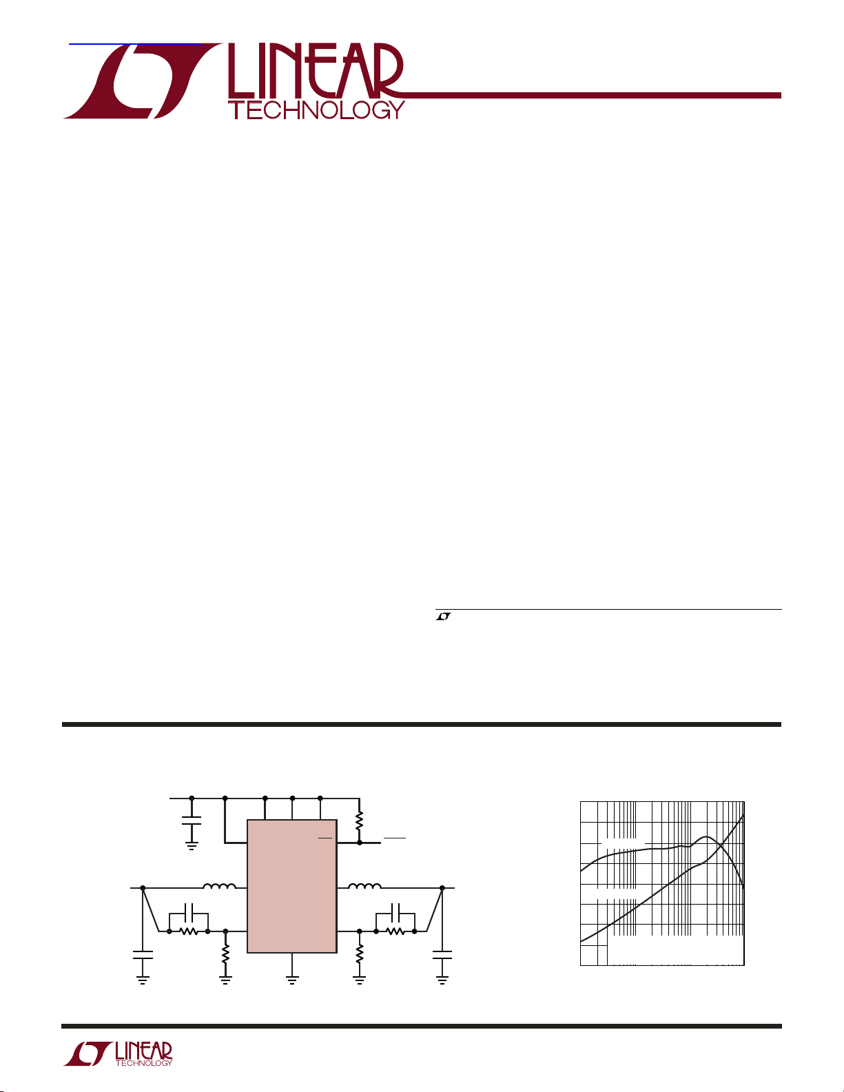
TYPICAL APPLICATIO
V
= 2.8V
IN
TO 5.5V
10µF
= 2.5V
V
OUT2
AT 400mA
4.7µF 10µF
887k 604k
Figure 1. 2.5V/1.8V at 400mA/800mA Step-Down Regulators
RUN2 V
MODE/SYNC
SW2
V
FB2
U
IN
LTC3548
GND
RUN1
POR
SW1
V
FB1
LTC3548 Efficiency Curve
100
100k
RESET
2.2µH4.7µH
33pF68pF
301k280k
V
= 1.8V
OUT1
AT 800mA
3548 TA01
95
90
85
80
POWER LOSS
75
EFFICIENCY (%)
70
65
60
1
EFFICIENCY
VIN = 3.3V, V
Burst Mode OPERATION
CHANNEL 1, NO LOAD ON CHANNEL 2
LOAD CURRENT (mA)
= 1.8V
OUT
10 100 1000
3548 TA02
1000
100
POWER LOSS (mW)
10
1
0.1
3548f
1
LTC3548
TOP VIEW
1
2
3
4
5
V
FB1
RUN1
V
IN
SW1
GND
10
9
8
7
6
V
FB2
RUN2
POR
SW2
MODE/
SYNC
11
MSE PACKAGE
10-LEAD PLASTIC MSOP
MSE PIN 11, EXPOSED PAD: PGND
MUST BE CONNECTED TO GND
WW
W
U
ABSOLUTE AXI U RATI GS
(Note 1)
VIN Voltages.................................................–0.3V to 6V
, V
V
FB1
, RUN1, RUN2
FB2
Voltages ..................................... – 0.3V to VIN + 0.3V
MODE/SYNC Voltage ...................... – 0.3V to V
SW1, SW2 Voltage ......................... – 0.3V to V
+ 0.3V
IN
+ 0.3V
IN
POR Voltage ................................................ – 0.3V to 6V
UUW
PACKAGE/ORDER I FOR ATIO
TOP VIEW
V
1
FB1
RUN1
2
11
3
V
IN
4
SW1
5
GND
10-LEAD (3mm × 3mm) PLASTIC DFN
T
JMAX
DD PACKAGE
DD PIN 11, EXPOSED PAD: PGND
MUST BE CONNECTED TO GND
= 125°C, θJA = 45°C/W, θJC = 3°C/W
(Soldered to a 4-layer board)
10
V
RUN2
9
POR
8
7
SW2
6
MODE/
SYNC
FB2
ORDER PART
NUMBER
LTC3548EDD
DD PART MARKING
LBNJ
Ambient Operating Temperature
Range (Note 2) ................................... –40°C to 85°C
Junction Temperature (Note 5)............................. 125°C
Storage Temperature Range ................. –65°C to 125°C
Lead Temperature (Soldering, 10 sec)
LTC3548EMSE only .......................................... 300°C
ORDER PART
NUMBER
LTC3548EMSE
MSE PART MARKING
LTBNH
T
= 125°C, θJA = 45°C/W, θJC = 10°C/W
JMAX
(Soldered to a 4-layer board)
Consult LTC Marketing for parts specified with wider operating temperature ranges.
ELECTRICAL CHARACTERISTICS
temperature range, otherwise specifications are at TA = 25°C. VIN = 3.6V, unless otherwise specified. (Note 2)
SYMBOL PARAMETER CONDITIONS MIN TYP MAX UNITS
V
IN
I
FB
V
FB
∆V
LINE REG
∆V
LOAD REG
I
S
f
OSC
f
SYNC
I
LIM
R
DS(ON)
I
SW(LKG)
2
The ● denotes the specifications which apply over the full operating
Operating Voltage Range ● 2.5 5.5 V
Feedback Pin Input Current ● 30 nA
Feedback Voltage (Note 3) 0°C ≤ TA ≤ 85°C 0.588 0.6 0.612 V
–40°C ≤ T
Reference Voltage Line Regulation VIN = 2.5V to 5.5V (Note 3) 0.3 0.5 %/V
Output Voltage Load Regulation (Note 3) 0.5 %
Input DC Supply Current
Active Mode V
Sleep Mode V
FB1
FB1
Shutdown RUN = 0V, V
Oscillator Frequency VFB = 0.6V ● 1.8 2.25 2.7 MHz
Synchronization Frequency 2.25 MHz
Peak Switch Current Limit Channel 1 VIN = 3V, VFB = 0.5V, Duty Cycle <35% 0.95 1.2 1.6 A
Peak Switch Current Limit Channel 2 V
IN
Top Switch On-Resistance (Note 6) 0.35 0.45 Ω
Bottom Switch On-Resistance (Note 6) 0.30 0.45 Ω
Switch Leakage Current VIN = 5V, V
≤ 85°C ● 0.585 0.6 0.612 V
A
= V
= 0.5V 700 950 µA
FB2
= V
= 0.63V, MODE/SYNC = 3.6V 40 60 µA
FB2
= 5.5V, MODE/SYNC = 0V 0.1 1 µA
IN
= 3V, VFB = 0.5V, Duty Cycle <35% 0.6 0.7 0.9 A
= 0V, VFB = 0V 0.01 1 µA
RUN
3548f
LTC3548
ELECTRICAL CHARACTERISTICS
temperature range, otherwise specifications are at T
The ● denotes the specifications which apply over the full operating
= 25°C. VIN = 3.6V, unless otherwise specified. (Note 2)
A
SYMBOL PARAMETER CONDITIONS MIN TYP MAX UNITS
POR Power-On Reset Threshold VFB Ramping Down, MODE/SYNC = 0V –8.5 %
Power-On Reset On-Resistance 100 200 Ω
Power-On Reset Delay 262,144 Cycles
V
RUN
I
RUN
Note 1: Absolute Maximum Ratings are those values beyond which the life
of a device may be impaired. No pin shall exceed 6V.
Note 2: The LTC3548 is guaranteed to meet specified performance from
0°C to 70°C. Specifications over the – 40°C and 85°C operating
temperature range are assured by design, characterization and correlation
with statistical process controls.
Note 3: The LTC3548 is tested in a proprietary test mode that connects
RUN Threshold ● 0.3 1 1.5 V
RUN Leakage Current ● 0.01 1 µA
to the output of the error amplifier.
V
FB
Note 4: Dynamic supply current is higher due to the internal gate charge
being delivered at the switching frequency.
Note 5: T
is calculated from the ambient TA and power dissipation P
J
D
according to the following formula: TJ = TA + (PD • θJA).
Note 6: The DFN switch on-resistance is guaranteed by correlation to
wafer level measurements.
UW
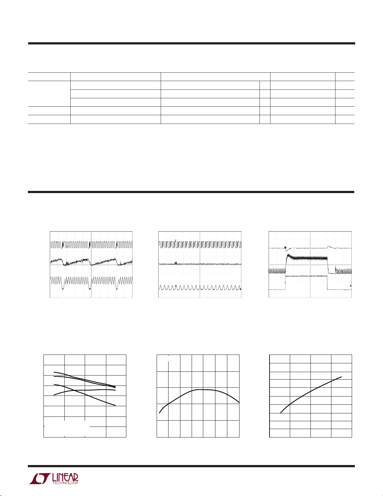
TYPICAL PERFOR A CE CHARACTERISTICS
TA = 25°C unless otherwise specified.
Load StepBurst Mode Operation Pulse Skipping Mode
SW
5V/DIV
V
OUT
20mV/DIV
I
L
200mA/DIV
VIN = 3.6V
= 1.8V
V
OUT
= 180mA
I
LOAD
CHANNEL 1; CIRCUIT OF FIGURE 3
Efficiency vs Input Voltage
100
95
90
85
80
75
EFFICIENCY (%)
70
V
65
Burst Mode OPERATION
CIRCUIT OF FIGURE 3
60
2
100mA
10mA
1mA
800mA
= 1.8V, CHANNEL 1
OUT
3
INPUT VOLTAGE (V)
SW
5V/DIV
V
OUT
10mV/DIV
I
L
200mA/DIV
2µs/DIV 1µs/DIV
3548 G01 3548 G02
V
= 3.6V
IN
= 1.8V
V
OUT
= 30mA
I
LOAD
CHANNEL 1; CIRCUIT OF FIGURE 3
Oscillator Frequency vs
Temperature
2.5
VIN = 3.6V
2.4
2.3
2.2
FREQUENCY (MHz)
2.1
456
3548 G04
2.0
–50 25 75
–25 0
TEMPERATURE (°C)
50 100 125
3548 G05
V
OUT
200mV/DIV
I
L
500mA/DIV
I
LOAD
500mA/DIV
V
= 3.6V
IN
= 1.8V
V
OUT
= 80mA TO 800mA
I
LOAD
CHANNEL 1; CIRCUIT OF FIGURE 3
Oscillator Frequency vs Supply
Voltage
10
8
6
4
2
0
–2
–4
FREQUENCY DEVIATION (%)
–6
–8
–10
2
20µs/DIV
3
SUPPLY VOLTAGE (V)
456
3548 G03
3548 G06
3548f
3
LTC3548
UW
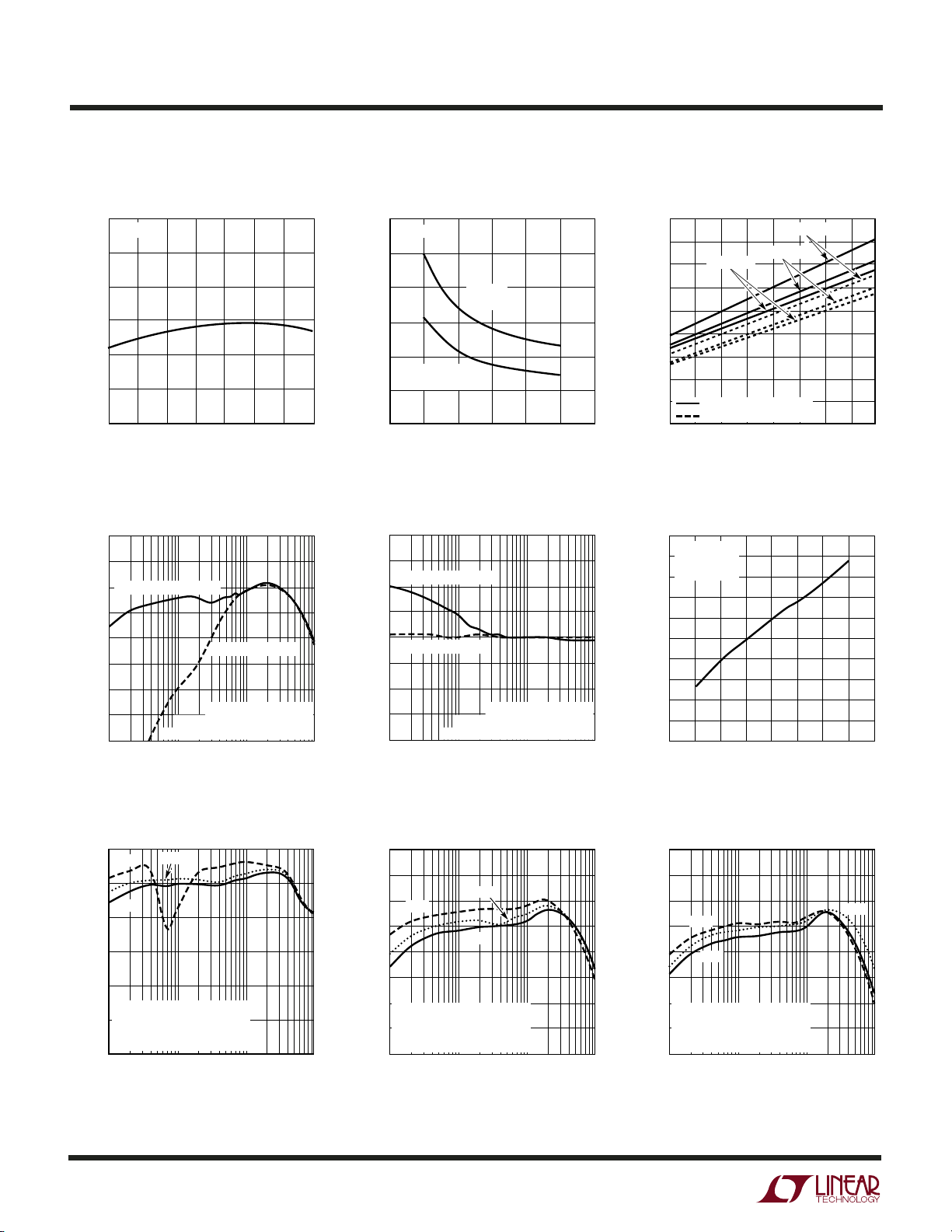
TYPICAL PERFOR A CE CHARACTERISTICS
Reference Voltage vs
Temperature R
0.615
VIN = 3.6V
0.610
0.605
0.600
0.595
REFERENCE VOLTAGE (V)
0.590
0.585
–50 25 75
–25 0
TEMPERATURE (°C)
50 100 125
3548 G07
500
450
400
(mΩ)
350
DS(ON)
R
300
250
200
1
vs Input Voltage R
DS(ON)
TA = 25°C
MAIN
SWITCH
SYNCHRONOUS
SWITCH
3
2
V
57
46
(V)
IN
3548 G08
550
500
450
400
350
(mΩ)
300
DS(ON)
R
250
200
150
100
vs Junction Temperature
DS(ON)
VIN = 4.2V
MAIN SWITCH
SYNCHRONOUS SWITCH
–50
–25 0
25 75
JUNCTION TEMPERATURE (°C)
VIN = 2.7V
VIN = 3.6V
50 100 150125
3548 G09
Efficiency vs Load Current
100
95
90
Burst Mode OPERATION
85
80
75
EFFICIENCY (%)
70
65
60
1
NO LOAD ON OTHER CHANNEL
CHANNEL 1; CIRCUIT OF FIGURE 3
10 100 1000
LOAD CURRENT (mA)
Efficiency vs Load Current
100
2.7V
90
80
70
EFFICIENCY (%)
60
V
50
Burst Mode OPERATION
NO LOAD ON OTHER CHANNEL
CIRCUIT OF FIGURE 3
40
1
3.6V
4.2V
= 2.5V, CHANNEL 1
OUT
10 100 1000
LOAD CURRENT (mA)
PULSE SKIP MODE
VIN = 3.6V, V
OUT
= 1.8V
3548 G11
3548 G10
Load Regulation
2.0
1.5
Burst Mode OPERATION
1.0
0.5
0
PULSE SKIP MODE
ERROR (%)
–0.5
OUT
V
–1.0
–1.5
–2.0
1
NO LOAD ON OTHER CHANNEL
CHANNEL 1; CIRCUIT OF FIGURE 3
10 100 1000
LOAD CURRENT (mA)
Efficiency vs Load Current
100
95
90
2.7V
85
80
75
EFFICIENCY (%)
70
V
= 1.5V, CHANNEL 1
OUT
Burst Mode OPERATION
65
NO LOAD ON OTHER CHANNEL
CIRCUIT OF FIGURE 3
60
1
3.6V
4.2V
10 100 1000
LOAD CURRENT (mA)
VIN = 3.6V, V
OUT
= 1.8V
3548 G12
3548 G14
Line Regulation
0.5
V
= 1.8V
OUT
0.4
= 200mA
I
OUT
= 25°C
T
A
0.3
0.2
0.1
0
ERROR (%)
–0.1
OUT
V
–0.2
–0.3
–0.4
–0.5
2
35
Efficiency vs Load Current
100
95
90
2.7V
85
80
75
EFFICIENCY (%)
70
65
60
4.2V
V
= 1.2V, CHANNEL 1
OUT
Burst Mode OPERATION
NO LOAD ON OTHER CHANNEL
CIRCUIT OF FIGURE 3
1
10 100 1000
LOAD CURRENT (mA)
4
VIN (V)
6
3548 G15
3.6V
3548 G13
4
3548f

LTC3548
U
UU
PI FU CTIO S
V
(Pin 1): Output Feedback. Receives the feedback
FB1
voltage from the external resistive divider across the
output. Nominal voltage for this pin is 0.6V.
RUN1 (Pin 2): Regulator 1 Enable. Forcing this pin to V
enables regulator 1, while forcing it to GND causes regulator 1 to shut down. This pin must be driven; do not float.
VIN (Pin 3): Main Power Supply. Must be closely decoupled
to GND.
SW1 (Pin 4): Regulator 1 Switch Node Connection to the
Inductor. This pin swings from VIN to GND.
GND (Pin 5): Main Ground. Connect to the (–) terminal of
C
, and (–) terminal of CIN.
OUT
MODE/SYNC (Pin 6): Combination Mode Selection and
Oscillator Synchronization. This pin controls the operation
of the device. When tied to VIN or GND, Burst Mode
operation or pulse skipping mode is selected, respectively. Do not float this pin. The oscillation frequency can
IN
be synchronized to an external oscillator applied to this pin
and pulse skipping mode is automatically selected.
SW2 (Pin 7): Regulator 2 Switch Node Connection to the
Inductor. This pin swings from VIN to GND.
POR (Pin 8): Power-On Reset . This common-drain logic
output is pulled to GND when the output voltage falls
below –8.5% of regulation and goes high after 117ms
when both channels are within regulation.
RUN2 (Pin 9): Regulator 2 Enable. Forcing this pin to V
enables regulator 2, while forcing it to GND causes regulator 2 to shut down. This pin must be driven; do not float.
V
(Pin 10): Output Feedback. Receives the feedback
FB2
voltage from the external resistive divider across the
output. Nominal voltage for this pin is 0.6V.
Exposed Pad (GND) (Pin 11): Power Ground. Connect to
the (–) terminal of C
connected to electrical ground on PCB.
, and (–) terminal of CIN. Must be
OUT
IN
3548f
5
 Loading...