

Linear Technology LTC3545EUD-1, LTC3545 Datasheet
LTC3545/LTC3545-1
1
35451fa
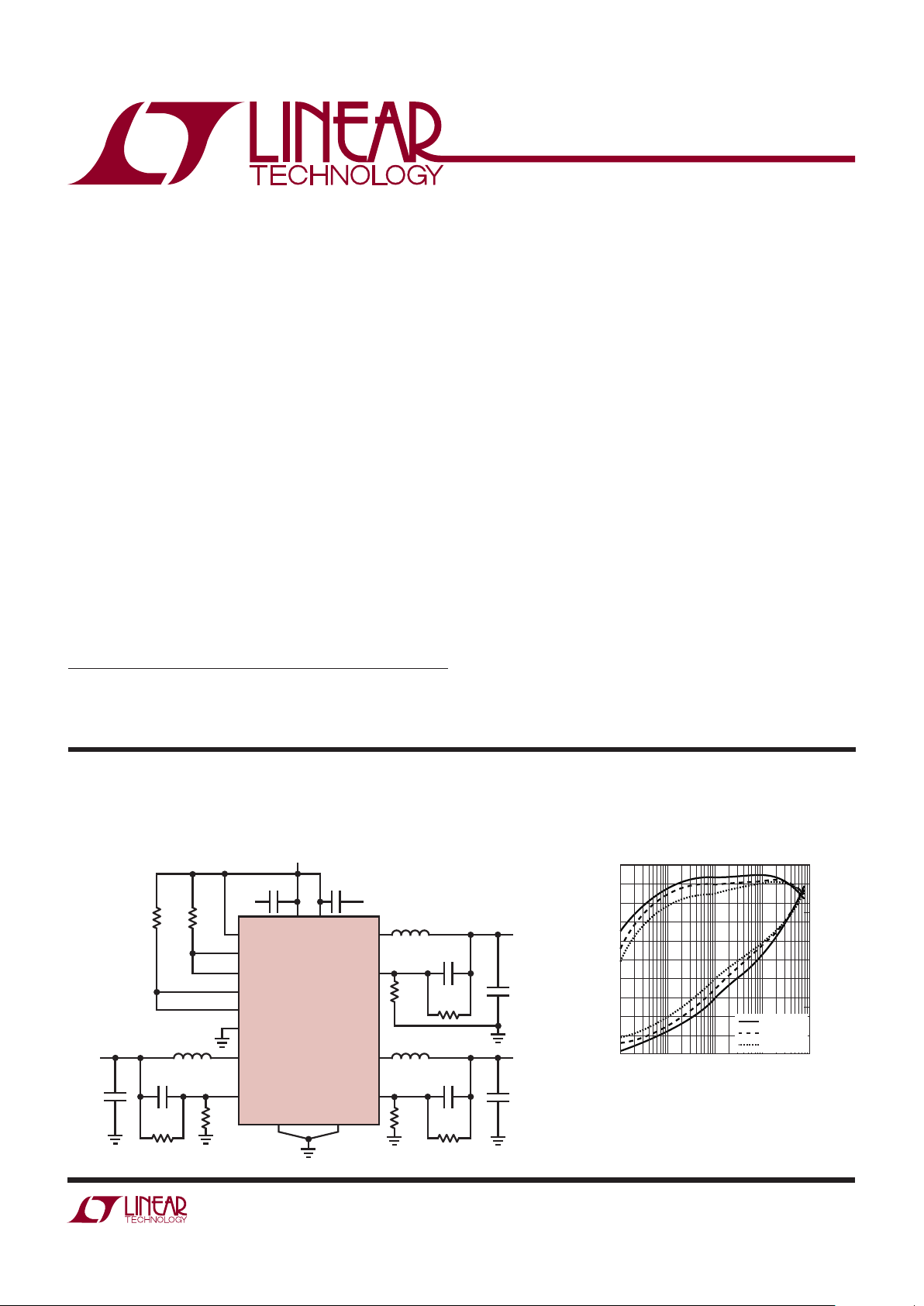
TYPICAL APPLICATION
FEATURES
APPLICATIONS
DESCRIPTION
Triple 800mA Synchronous
Step-Down Regulator–2.25MHz
The LTC®3545/LTC3545-1 are triple, high efficiency,
monolithic synchronous buck regulators using a constant
frequency, current mode architecture. The regulators operate independently with separate run pins. The 2.25V to
5.5V input voltage range makes the LTC3545/LTC3545-1
well suited for single Li-Ion battery-powered applications.
Low ripple pulse skip mode or high effi ciency Burst Mode
operation is externally selectable. PWM pulse skip mode
operation provides very low output ripple voltage while
Burst Mode operation increases effi ciency at low output
loads.
Switching frequency is internally set to 2.25MHz, or the
switching frequency can be synchronized to an external
1MHz to 3MHz clock. Power good indicators easily allow
power on sequencing between the three regulators.
The internal synchronous switches increase effi ciency and
eliminate external Schottky diodes. Low output voltages are
supported with the 0.6V feedback reference voltage.
The LTC3545-1 replaces the SYNC/MODE function with a
third PGOOD pin and forces Burst Mode operation.
■
Three 800mA Outputs
■
High Effi ciency: Up to 95%
■
2.25V to 5.5V Input Voltage Range
■
Low Ripple (<20mV
P-P
) Burst Mode® Operation
I
Q
: 58μA
■
2.25MHz Constant Frequency Operation or
■
Synchronizable to External 1MHz to 3MHz Clock
■
Power Good Indicators Ease Supply Sequencing
■
0.6V Reference Allows Low Output Voltages
■
Current Mode Operation/Excellent Transient Response
■
Low Profi le 16-Lead 3mm × 3mm QFN Package
■
Smart Phones
■
Wireless and DSL Modems
■
Digital Still Cameras
■
Portable Instruments
■
Point of Load Regulation
High Effi ciency Triple Step-Down Converter with Power Sequencing
Effi ciency and Loss vs Load Current
L, LT, LTC, LTM and Burst Mode are registered trademarks of Linear Technology Corporation.
All other trademarks are the property of their respective owners.
Protected by U.S. Patents including 6580258, 5481178, 6127815, 6498466, 6611131.
3545 TA01
L1
1.5µH
C5
10µF
PGNDGNDA
C4 10µF
C6
20pF
R2
255k
R1
511k
C1
10µF
V
OUT1
1.8V
V
IN
2.25V TO 5.5V
RUN1
PGOOD1
RUN2
PGOOD2
RUN3
L2
1.5µH
R4
226k
C2
10µF
V
OUT2
1.2V
SW2
V
FB2
SYNC/MODE
SW1
V
FB1
VINPV
IN
LTC3545
GNDA PGND
R7
500k
C7
20pF
R3
226k
R8
500k
L3
1.5µH
R6
200k
C3
10µF
V
OUT3
1.5V
SW3
V
FB3
C8
20pF
R5
301k
LOAD CURRENT (A)
30
EFFICIENCY (%)
LOSS (W)
90
100
20
10
80
50
70
60
40
0.0001 0.01 0.1 1
3545 TA01b
0
0.001
1
0.1
0.01
0.0001
0.001
VIN = 2.5V
V
IN
= 3.6V
V
IN
= 4.2V
TA = 25°C
V
OUT
= 2V
Burst Mode OPERATION
f
OSC
= 2.25MHz
SINGLE CHANNEL
LTC3545/LTC3545-1
2
35451fa
ELECTRICAL CHARACTERISTICS
ABSOLUTE MAXIMUM RATINGS
Input Supply Voltage .................................... –0.3V to 6V
RUNx, PGOODx ..............................–0.3V to (V
IN
+ 0.3V)
V
FBx
, SYNC/MODE .........................–0.3V to (VIN + 0.3V)
SWx ...............................................–0.3V to (V
IN
+ 0.3V)
P-Switch Source Current (DC) (Note 8) ...................1.1A
(Note 1)
SYMBOL PARAMETER CONDITIONS MIN TYP MAX UNITS
General Characteristics
V
IN
Input Voltage Range
●
2.25 5.5 V
V
FBx
Regulated Feedback Voltage (Note 5) TA = 25°C,
0°C ≤ T
A
≤ 85°C
●
0.592
0.588
0.6
0.6
0.608
0.612
V
V
ΔV
FBx
Reference Voltage Line Regulation (Note 5) VIN = 2.25V to 5.5V
●
0.08 0.15 %/V
V
LOADREG
Output Voltage Load Regulation (Note 6) 0.5 %
The ● denotes the specifi cations which apply over the full operating
temperature range, otherwise specifi cations are at TA = 25°C. VIN = 3.6V unless otherwise noted. (Note 2)
N-Channel Sink Current (DC) (Note 8) .....................1.1A
Peak SW Sink and Source Current (Note 8) .............1.3A
Operating Temperature Range.................. –40°C to 85°C
Junction Temperature (Notes 3, 4)........................ 125°C
Storage Temperature Range ...................–65°C to 125°C
16 15 14 13
5 6 7 8
17
UD PACKAGE
16-LEAD (3mm s 3mm) PLASTIC QFN
TOP VIEW
9
10
11
12
4
3
2
1SW1
PGOOD1
RUN2
PGOOD2
V
FB2
V
FB3
RUN3
SYNC/MODE
GNDA
VINRUN1
V
FB1
SW2
PGND
PV
IN
SW3
T
JMAX
= 125°C, θJA = 68°C/W
EXPOSED PAD (PIN 17) IS GND, MUST BE SOLDERED TO PCB
16 15 14 13
5 6 7 8
TOP VIEW
17
UD PACKAGE
16-LEAD (3mm s 3mm) PLASTIC QFN
9
10
11
12
4
3
2
1SW1
PGOOD1
RUN2
PGOOD2
V
FB2
V
FB3
RUN3
PGOOD3
GNDA
VINRUN1
V
FB1
SW2
PGND
PV
IN
SW3
T
JMAX
= 125°C, θJA = 68°C/W
EXPOSED PAD (PIN 17) IS GND, MUST BE SOLDERED TO PCB
PIN CONFIGURATION
LEAD FREE FINISH TAPE AND REEL PART MARKING PACKAGE DESCRIPTION TEMPERATURE RANGE
LTC3545EUD#PBF
LTC3545EUD-1#PBF
LTC3545EUD#TRPBF
LTC3545EUD-1#TRPBF
LCSR
LDDP
16-Lead (3mm × 3mm) Plastic QFN
16-Lead (3mm × 3mm) Plastic QFN
–40°C to 85°C
–40°C to 85°C
Consult LTC Marketing for parts specifi ed with wider operating temperature ranges.
Consult LTC Marketing for information on non-standard lead based fi nish parts.
For more information on lead free part marking, go to: http://www.linear.com/leadfree/
For more information on tape and reel specifi cations, go to: http://www.linear.com/tapeandreel/
ORDER INFORMATION
LTC3545 LTC3545-1

LTC3545/LTC3545-1
3
35451fa
Note 1: Stresses beyond those listed under Absolute Maximum Ratings
may cause permanent damage to the device. Exposure to any Absolute
Maximum Rating condition for extended periods may affect device
reliability and lifetime.
Note 2: The LTC3545/LTC3545-1 are guaranteed to meet performance
specifi cations from 0°C to 85°C. Specifi cations over the –40°C to 85°C
operating temperature range are assured by design, characterization and
correlation with statistical process controls.
Note 3: T
J
is calculated from the ambient temperature TA and power
dissipation P
D
according to the following formula:
T
J
= TA + (PD)(68°C/W)
This IC includes overtemperature protection that is intended to protect
the device during momentary overload conditions. Junction temperature
will exceed 125°C when overtemperature is active. Continuous operation
above the specifi ed maximum operating junction temperature may impair
device reliability.
SYMBOL PARAMETER CONDITIONS MIN TYP MAX UNITS
I
FB
Feedback Pin Leakage 80 nA
I
S
Input DC Bias Current Active Mode (Pulse Skip)
Burst Mode (All Regulators Sleeping)
Shutdown
VFB = 0.5V or V
OUT
= 90%, I
LOAD
= 0A,
2.25MHz, Three Regulators Enabled,
680
58
0.1
750
70
2.0
µA
µA
µA
f
OSC
Oscillator Frequency
●
1.8 2.25 2.7 MHz
f
SYNC
Synchronization Frequency LTC3545 Only
●
13MHz
V
RUN(HIGH)
RUNx Input High Voltage
●
1V
V
RUN(LOW)
RUNx Input Low Voltage
●
0.3 V
I
RUN
RUN Leakage Current ±0.1 ±1 µA
I
LSW
SWx Leakage V
RUN
= 0V, VSW = 0V or 5.5V, VIN = 5.5V ±0.1 ±1 µA
I
SYNC
SYNC Leakage V
RUNx
= 0V, V
SYNC
= 0V or 5.5V,
V
IN
= 5.5V
±0.1 ±1 µA
T
PGOOD
Power Good Threshold–Deviation From VFB
Steady State (0.6V)
V
FBx
Ramping Up
V
FBx
Ramping Down
–7.5
–10
%
%
R
PGOOD
Power Good Pull-Down On-Resistance I
PGD
= 50mA
●
14 50
Ω
MODE/SYNC Thresholds 0.93 V
Individual Regulator Characteristics
t
SS
Soft-Start Period VFB = 10% to 90% Fullscale 850 1100 µs
I
PK
Peak Switch Current Limit VFB < V
FBREG
, Duty Cycle < 35% 1 1.3 1.6 A
I
Q
Input DC Bias Current Active Mode (Pulse Skip)
Burst Mode Operation
VFB = 0.5V, I
LOAD
= 0A, 2.25MHz 310
31
µA
µA
R
PFET
R
DS(ON)
of P-Channel FET (Note 7) ISW = 100mA 0.35
Ω
R
NFET
R
DS(ON)
of N-Channel FET (Note 7) ISW = –100mA 0.35
Ω
V
UVLO
Undervoltage Lockout (High VCC to Low)
●
1.8 2.25 V
ELECTRICAL CHARACTERISTICS
The ● denotes the specifi cations which apply over the full operating
temperature range, otherwise specifi cations are at T
A
= 25°C. VIN = 3.6V unless otherwise noted. (Note 3)
Note 4: This IC includes overtemperature protection that is intended
to protect the device during momentary overload conditions. Junction
temperature will exceed 125°C when overtemperature is active.
Continuous operation above the specifi ed maximum operating junction
temperature may impair device reliability.
Note 5: The LTC3545/LTC3545-1 are tested in a proprietary test mode that
connects V
FB
to the output of the error amplifi er.
Note 6: Load regulation is inferred by measuring the regulation loop gain.
Note 7: The QFN switch-on resistance is guaranteed by correlation to
water level measurements.
Note 8: Guaranteed by long-term current density limitations.

LTC3545/LTC3545-1
4
35451fa
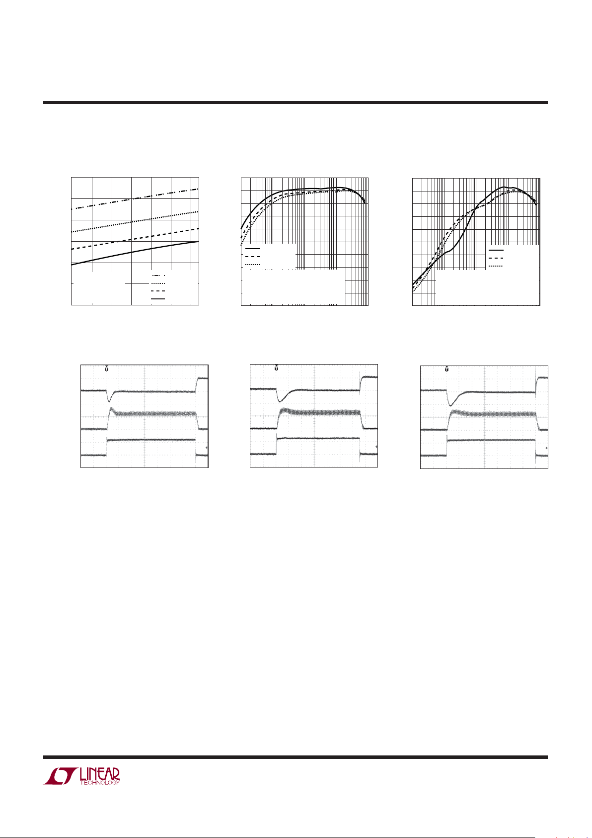
Burst Mode Operation Effi ciency vs Supply Voltage
Supply Current vs Temperature
Burst Mode Operation
TYPICAL PERFORMANCE CHARACTERISTICS
V
REF
vs Temperature at 2.25V,
3.6V, 5.5V
Switching Frequency vs Supply
Voltage and Temperature Load Regulation, All Channels
TEMPERATURE (°C)
–50
0.585
V
REF
(V)
0.590
0.595
0.600
0.605
0.610
0.615
0 50 100
3545 G01
2.25V
3.6V
5.5V
SUPPLY VOLTAGE (V)
2
1.5
SWITCHING FREQUENCY (MHz)
2.0
2.5
3.0
34
3545 G02
56
f
OSC
= –40°C
f
OSC
= 0°C
f
OSC
= 25°C
f
OSC
= 80°C
LOAD CURRENT (mA)
0
0.6
0.8
1.2
600
3545 G03
0.4
0.2
200 400 800
0
–0.4
–0.2
1.0
V
OUT
ERROR (%)
CHANNEL 1
CHANNEL 2
CHANNEL 3
TA = 25°C
V
IN
= 3.6V
UNTESTED CHANNELS OFF
PULSE SKIP MODE
1µs/DIV
SW
2V/DIV
I
L
100mA/DIV
V
OUT
20mV/DIV
3545 G04
VIN = 3.6V
V
OUT
= 1.8V
I
LOAD
= 50mA
f
OSC
= 2.25MHz
SUPPLY VOLTAGE (V)
2
EFFICIENCY (%)
90
95
6
3545 G05
85
80
3
4
5
100
V
OUT
= 2V
T
A
= 25°C
CHANNEL 3, ALL OTHERS OFF
f
OSC
= 2.25MHz
I
LOAD
= 250mA
TEMPERATURE (°C)
–40
0
SUPPLY CURRENT (µA)
5
15
20
25
40
45
3545 G06
10
0
–20
60
20 80
30
35
40
VIN = 5.5V
V
IN
= 4.5V
V
IN
= 3.5V
V
IN
= 2.5V
TA = 25°C
V
FB3
= 0.625V
I
LOAD
= 0V
CHANNEL 3 ONLY
LTC3545/LTC3545-1
5
35451fa
TYPICAL PERFORMANCE CHARACTERISTICS
Channel 1 Load Step Response Channel 2 Load Step Response Channel 3 Load Step Response
Supply Current vs Temperature,
Pulse Skipping
Effi ciency vs Load Current,
Burst Mode Operation
Effi ciency vs Load Current,
Pulse Skipping Operation
TEMPERATURE (°C)
–40
150
SUPPLY CURRENT (µA)
200
250
300
350
450
–20
02040
3545 G07
60 80
400
TA = 25°C
V
FB3
= 0.625V
I
LOAD
= 0V
CHANNEL 3 ONLY
VIN = 5.5V
V
IN
= 4.5V
V
IN
= 3.5V
V
IN
= 2.5V
LOAD CURRENT (mA)
30
EFFICIENCY (%)
90
100
20
10
80
50
70
60
40
0.1 10 100 1000
3545 G08
0
1
VIN = 2.7V
V
IN
= 3.6V
V
IN
= 4.2V
TA = 25°C
V
OUT
= 1.8V
CHANNEL 3, OTHER CHANNELS OFF
f
OSC
= 2.25MHz
LOAD CURRENT (mA)
30
EFFICIENCY (%)
90
100
20
10
80
50
70
60
40
0.1 10 100 1000
3545 G09
0
1
VIN = 2.7V
V
IN
= 3.6V
V
IN
= 4.2V
TA = 25°C
V
OUT
= 1.8V
CHANNEL 3, OTHER CHANNELS OFF
f
OSC
= 2.25MHz
10µs/DIV
I
LOAD
500mA/DIV
I
L
500mA/DIV
V
OUT1
100mV/DIV
3545 G10
TA = 25°C
V
IN
= 3.6V
V
OUT
= 1.2V
LOAD STEP 0mA TO 600mA
Burst Mode OPERATION
10µs/DIV
I
LOAD
500mA/DIV
I
L
500mA/DIV
V
OUT2
100mV/DIV
3545 G11
TA = 25°C
V
IN
= 3.6V
V
OUT
= 1.5V
LOAD STEP 0mA TO 600mA
Burst Mode OPERATION
10µs/DIV
I
LOAD
500mA/DIV
I
L
500mA/DIV
V
OUT3
100mV/DIV
3545 G12
TA = 25°C
V
IN
= 3.6V
V
OUT
= 1.8V
LOAD STEP 0mA TO 600mA
Burst Mode OPERATION
LTC3545/LTC3545-1
6
35451fa
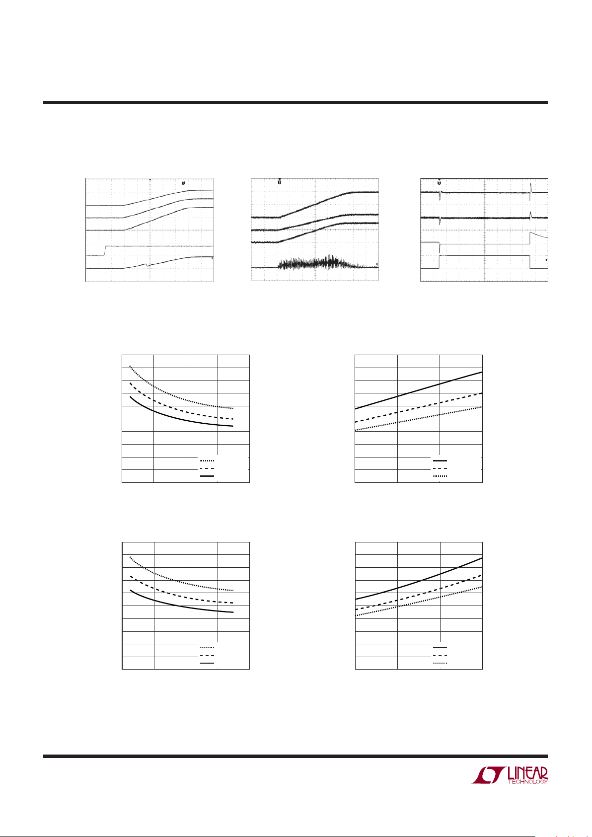
TYPICAL PERFORMANCE CHARACTERISTICS
Start-Up From Shutdown
Loaded
PFET R
DS(ON)
vs Supply Voltage PFET R
DS(ON)
vs Temperature
NFET R
DS(ON)
vs Supply Voltage
Start-Up From Shutdown
No Load Load Step Crosstalk
NFET R
DS(ON)
vs Temperature
200µs/DIV
I
SUPPLY
1A/DIV
RUNX
5V/DIV
V
OUT1
V
OUT2
V
OUT3
(ALL 1V/DIV)
3545 G13
TA = 25°C
V
IN
= 3.6V
I
LOAD
= 600mA, ALL CHANNELS
200µs/DIV
I
SUPPLY
50mA/DIV
V
OUT1
1V/DIV
V
OUT2
1V/DIV
V
OUT3
1V/DIV
3545 G14
TA = 25°C
V
IN
= 3.6V
I
LOAD
= 0, ALL CHANNELS
200µs/DIV
I
LOAD
CH1
50mA/DIV
V
OUT2
2mV/DIV
V
OUT3
2mV/DIV
V
OUT1
100mV/DIV
3545 G15
TA = 25°C
V
IN
= 3.6V
500mA LOAD STEP IN CHANNEL1
CHANNELS 2 AND 3 LOADED AT 400mA EACH
SUPPLY VOLTAGE (V)
2
0
R
DS(ON)
()
0.05
0.15
0.20
0.25
0.50
0.35
3
4
3545 G16
0.10
0.40
0.45
0.30
5
6
TA = 85°C
T
A
= 25°C
T
A
= –25°C
TEMPERATURE (°C)
–50
0
R
DS(ON)
()
0.05
0.15
0.20
0.25
0.50
0.35
0
3545 G17
0.10
0.40
0.45
0.30
50
100
VIN = 2.5V
V
IN
= 3.6V
V
IN
= 5.5V
SUPPLY VOLTAGE (V)
2
0
R
DS(ON)
()
0.05
0.15
0.20
0.25
0.50
0.35
3
4
3545 G18
0.10
0.40
0.45
0.30
5
6
TA = 85°C
T
A
= 25°C
T
A
= –25°C
TEMPERATURE (°C)
–50
0
R
DS(ON)
()
0.05
0.15
0.20
0.25
0.50
0.35
0
3545 G19
0.10
0.40
0.45
0.30
50
100
VIN = 2.5V
V
IN
= 3.6V
V
IN
= 5.5V
 Loading...