

FEATURES
LTC3454
1A Synchronous Buck-Boost
High Current LED Driver
U
DESCRIPTIO
■
High Effi ciency: >90% Typical in Torch Mode,
>80% in Flash Mode
■
Wide VIN Range: 2.7V to 5.5V
■
Up to 1A Continuous Output Current
■
3.5% LED Current Programming Accuracy
■
Internal Soft-Start
■
Open/Shorted LED Protection
■
Constant Frequency 1MHz Operation
■
Zero Shutdown Current
■
Overtemperature Protection
■
Small Thermally Enhanced 10-Lead (3mm × 3mm)
DFN Package
U
APPLICATIO S
■
Cell Phone Camera Flash
■
Cell Phone Torch Lighting
■
Digital Cameras
■
PDAs
■
Misc Li-Ion LED Drivers
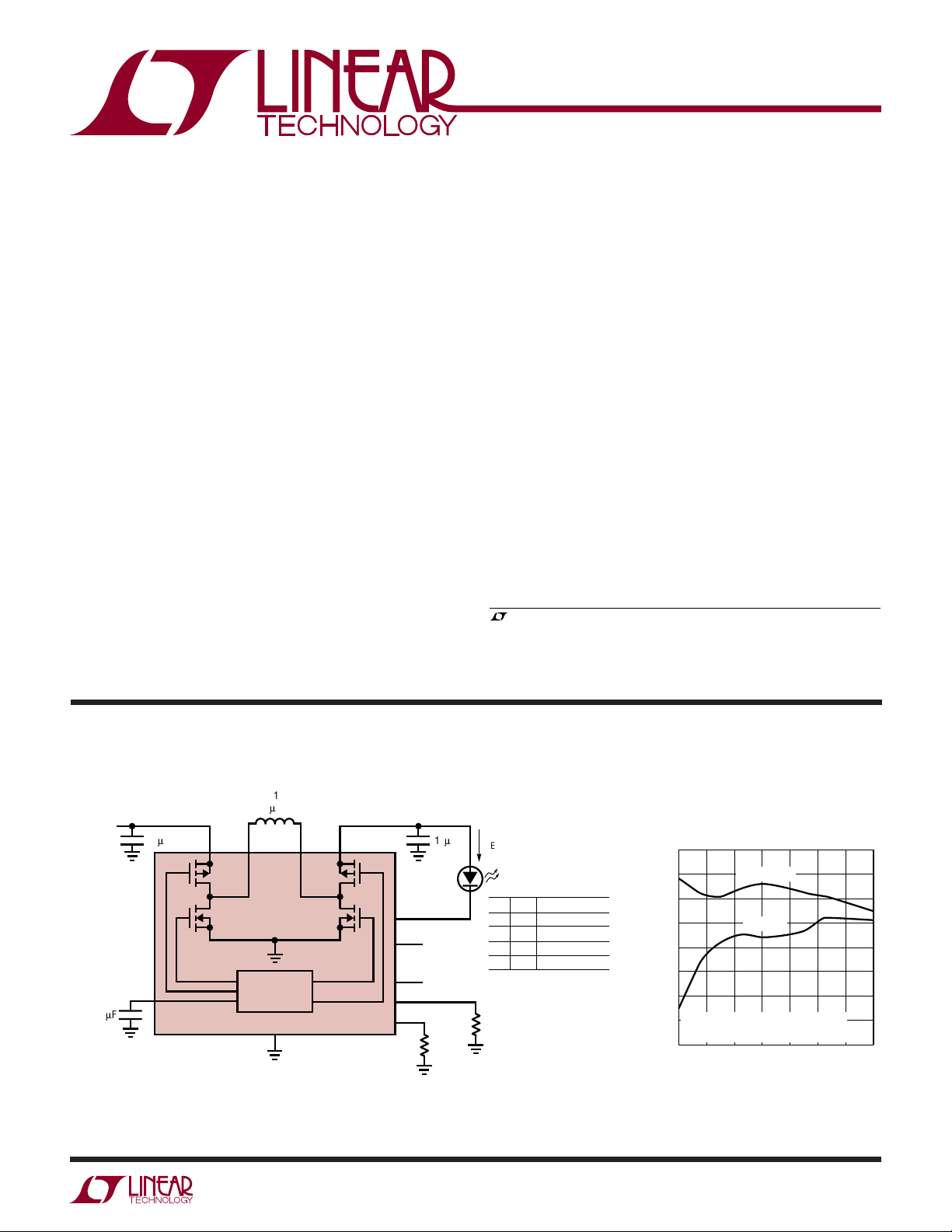
The LTC®3454 is a synchronous buck-boost DC/DC
converter optimized for driving a single high power LED
at currents up to 1A from a single cell Li-Ion battery input. The regulator operates in either synchronous buck,
synchronous boost, or buck-boost mode depending on
input voltage and LED forward voltage. P
LED/PIN
effi ciency
greater than 90% can be achieved over the entire usable
range of a Li-Ion battery (2.7V to 4.2V).
LED current is programmable to one of four levels, including shutdown, with dual external resistors and dual enable
inputs. In shutdown no supply current is drawn.
A high constant operating frequency of 1MHz allows the
use of small external components. The LTC3454 is offered
in a low profi le (0.75mm) thermally enhanced 10-lead
(3mm × 3mm) DFN package.
, LTC and LT are registered trademarks of Linear Technology Corporation.
All other trademarks are the property of their respective owners.
TYPICAL APPLICATIO
High Effi ciency Torch/Flash LED Driver
V
1-CELL
Li-Ion
2.7V-4.2V
0.1mF
IN
10mF
V
C
LED: LUMILEDS LXL-PWF1
L1: SUMIDA CDRH6D28-5RONC
V
IN
A
B
L1
5mH
SW1
1MHz
BUCK-BOOST
GND (EXPOSED PAD)
U
SW2 V
D
C
OUT
LTC3454
LED
I
SET1
I
SET2
10mF
LED
EN1 (TORCH)
EN2 (FLASH)
R
ISET2
3.65k
1%
I
LED
EN2 EN1 I
0 0 0 (SHUTDOWN)
0 1 150mA
1 0 850mA
111A
R
ISET1
20.5k
1%
3453 TA01a
LED
LED Power Effi ciency vs V
100
I
= 150mA
95
90
85
80
75
EFFICIENCY (%)
70
TA = 25°C
65
EFFICIENCY = (V
60
2.7
LED
I
LED
OUT
3.1 3.93.5 4.7
= 1A
– V
LED)ILED/VINIIN
4.3
(V)
V
IN
IN
5.55.1
3454 TA01b
3454f
1
LTC3454
WW
W
ABSOLUTE AXI U RATI GS
(Note 1)
VIN, SW1, SW2, V
, EN1, EN2, I
V
C
Voltage .............................– 0.3V to (V
LED Peak Current ...................................................1.25A
Storage Temperature Range ...................–65°C to 125°C
Operating Temperature Range (Note 2) ...–40°C to 85°C
Junction Temperature (Note 3) ............................. 125°C
Voltage ......................–0.3V to 6V
OUT
, I
SET2
SET1
U
+ 0.3V) or 6V
IN
UUW
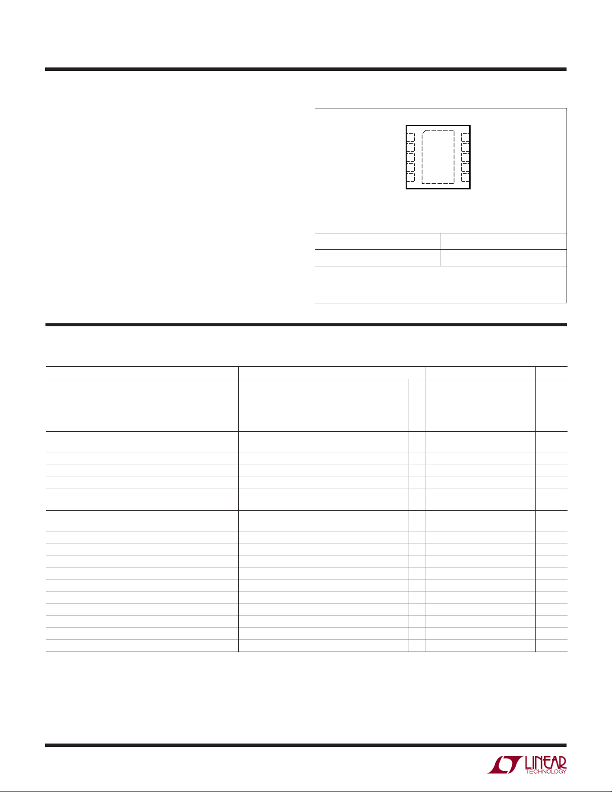
PACKAGE/ORDER I FOR ATIO
TOP VIEW
10
EN1
1
EN2
2
3
I
SET1
4
I
SET2
5
LED
10-LEAD (3mm × 3mm) PLASTIC DFN
EXPOSED PAD (PIN 11) IS GND, MUST BE SOLDERED TO PCB
DD PACKAGE
T
= 125°C, θJA = 40°C/W
JMAX
SW1
V
9
IN
V
811
C
7
V
OUT
6
SW2
ORDER PART NUMBER DD PART MARKING
LTC3454EDD
Order Options Tape and Reel: Add #TR
Lead Free: Add #PBF Lead Free Tape and Reel: Add #TRPBF
Lead Free Part Marking: http://www.linear.com/leadfree/
Consult LTC Marketing for parts specifi ed with wider operating temperature ranges.
●
The
ELECTRICAL CHARACTERISTICS
temperature range, otherwise specifi cations are at T
= 25°C, VIN = 3.6V, R
A
PARAMETER CONDITIONS MIN TYP MAX UNITS
Input Supply Voltage (V
)
IN
Input DC Supply Current (Typicals at V
Normal Operation 2.7V ≤ V
Shutdown 2.7V ≤ V
UVLO V
Undervoltage Lockout Threshold V
VIN Falling 1.75 1.90 V
V
, V
EN1
V
EN1
V
EN1
I
SET1
788 800 812 mV
DC Threshold for Normal Operation (VIH)
EN2
, V
DC Threshold for Shutdown (VIL)
EN2
, V
Input Current
EN2
and I
Servo Voltage 3.08k ≤ R
SET2
LED Output Current to Programming Current Ratio I
3775 3850 3925 mA/mA
LED Pin Voltage I
Regulated Maximum V
PMOS Switch R
NMOS Switch R
ON
ON
LED Pin Open, Programmed I
OUT
Switches A and D (V
Switches B and C 130 mΩ
< UVLO Threshold; V
IN
Rising
IN
/(I
LED
ISET1
= 1A 105 mV
LED
Forward Current Limit Switch A 2.5 3.4 A
Reverse Current Limit Switch D (V
PMOS Switch Leakage Switches A, D –1 1 µA
NMOS Switch Leakage Switches B, C –1 1 µA
Oscillator Frequency 0.9 1.0 1.15 MHz
Soft-Start Time 200 µs
Note 1: Absolute Maximum Ratings are those values beyond which the life
of a device may be impaired.
Note 2: The LTC3454 is guaranteed to meet specifi cations from 0°C to
70°C. Specifi cations over the –40°C to 85°C operating temperature range
are assured by design, characterization and correlation with statistical
process controls.
denotes the specifi cations which apply over the full operating
= 20.5k unless otherwise noted. (Note 2)
ISET
●
2.7 5.5 V
= 3.6V, R
IN
≤ 5.5V (Note 4)
IN
≤ 5.5V; V
IN
ISET1
EN1
||R
ISET2
+ I
), I
ISET2
OUT
= 3.6V) 275 mA
OUT
= R
ISET1
= V
EN2
= V
EN1
≤ 20.5k
= 500mA (Note 5)
LED
LED
= 20.5k)
ISET2
= 0V 0 1 µA
= VIN 5 10 µA
EN2
●
2.05 2.3 V
●
0.68 1.2 V
●
0.2 0.66 V
●
–1 1 µA
●
780 800 812 mV
●
3725 3850 3975 mA/mA
= 1A
●
4.95 5.15 5.35 V
= 3.6V) 170 mΩ
Note 3: T
is calculated from the ambient temperature TA and power
J
dissipation PD according to the following formula:
T
= TA + (PD • θJA °C/W).
J
Note 4: Dynamic supply current is higher due to the gate charge being
delivered at the switching frequency.
Note 5: This parameter is tested using a feedback loop which servos V
to 1.8V.
LBQX
825 1200 µA
C
3454f
2
UW
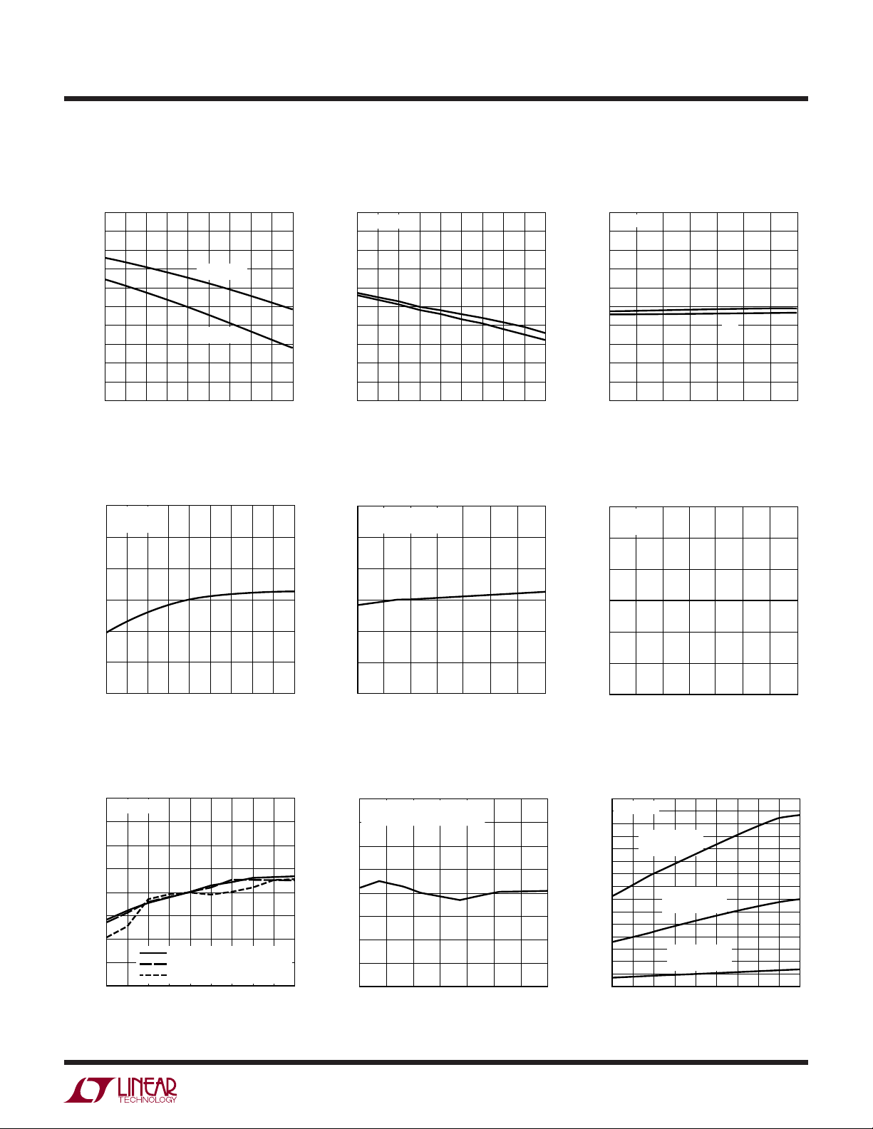
TYPICAL PERFOR A CE CHARACTERISTICS
LTC3454
Undervoltage Lockout Threshold
vs Temperature
2.4
2.3
2.2
2.1
2.0
1.9
1.8
1.7
UVLO THRESHOLD (V)
1.6
1.5
1.4
–35 5
–15
–55
I
Servo Voltage
SET1,2
VIN RISING
VIN FALLING
45 125
65
25
TEMPERATURE (°C)
vs Temperature
812
VIN = 3.6V
= 15k
R
ISET1,2
808
804
(mV)
800
ISET1,2
V
796
Enable Thresholds
vs Temperature
1200
VIN = 3.6V
1100
1000
900
800
700
600
500
ENABLE THRESHOLDS (mV)
400
300
85
105
3454 G01
200
812
808
804
(mV)
800
ISET1,2
V
796
–35 5
–15
–55
I
Servo Voltage vs V
SET1,2
TA = 25°C
= R
R
ISET1
ISET2
45 125
25
TEMPERATURE (°C)
= 15k
V
IH
V
IL
85
105
65
3454 G02
IN
Enable Thresholds vs V
1200
TA = 25°C
1100
1000
900
800
700
600
500
ENABLE THRESHOLDS (mV)
400
300
200
3.1 3.9
3.5 5.5
Servo Voltage vs R
VIN = 3.6V
= 25°C
T
A
812
808
804
(mV)
800
ISET1,2
V
796
2.7
I
SET1,2
VIN (V)
4.3
IN
V
IH
V
IL
4.7
5.1
3454 G03
ISET
792
788
–35 5
–55
–15
TEMPERATURE (°C)
45 125
25
LED Current Programming Ratio
vs Temperature
4050
VIN = 3.6V
4000
3950
3900
3850
RATIO
3800
3750
3700
3650
–35 125
–55
PROGRAMMED I
PROGRAMMED I
PROGRAMMED I
–15
25
5
TEMPERATURE (°C)
45
65
65
85
LED
LED
LED
85
105
3454 G04
= 1A
= 500mA
= 150mA
105
3454 G07
792
788
2.7
3.1 3.5
4.3 5.1 5.5
3.9 4.7
VIN (V)
LED Current Programming Ratio
vs V
IN
4050
4000
3950
3900
3850
RATIO
3800
3750
3700
3650
PROGRAMMED I
= 25°C
T
A
3.1 5.5
2.7
LED
3.9 4.7
3.5
= 500mA
4.3
VIN (V)
3454 G05
5.1
3454 G08
792
788
150
120
(mV)
LED
V
3
711
vs Temperature
V
LED
VIN = 3.6V
90
60
30
0
–55
–35 –15
19 27 31
15 23
R
(kΩ)
ISET
PROGRAMMED
= 1A
I
LED
PROGRAMMED
= 500mA
I
LED
PROGRAMMED
= 100mA
I
LED
25
5 45 125
TEMPERATURE (°C)
3454 G06
65 85 105
3454 G09
3454f
3

LTC3454
UW
TYPICAL PERFOR A CE CHARACTERISTICS
V
vs V
60
58
56
54
52
(mV)
50
LED
V
48
46
44
42
40
2.7
LED
PROGRAMMED I
T
= 25°C
A
3.1
3.5
IN
= 500mA
LED
4.3
3.9
VIN (V)
Maximum Regulated V
vs Programmed LED Current
5.40
VIN = 3.6V
5.35
= 25°C
T
A
5.30
5.25
5.20
(V)
5.15
OUT
V
5.10
5.05
5.00
4.95
4.90
200 1000
100
300
500
600
400
PROGRAMMED I
LED
700
4.7
OUT
(mA)
800
5.1
3454 G10
5.5
Maximum Regulated V
vs Temperature
5.40
PROGRAMMED I
5.35
= 3.6V
V
IN
5.30
5.25
5.20
(V)
5.15
OUT
V
5.10
5.05
5.00
4.95
4.90
–35 125
–55
–15
= 1A
LED
25
5
TEMPERATURE (°C)
OUT
45
105
65
85
Maximum Regulated V
vs V
IN
5.40
PROGRAMMED I
5.35
= 25°C
T
A
5.30
5.25
5.20
(V)
5.15
OUT
V
5.10
5.05
5.00
4.95
4.90
2.7
3.1
3.5
LED
3.9
= 1A
4.3
VIN (V)
OUT
4.7
5.1
5.5
3454 G12
900
3454 G13
PMOS R
300
MEASURED AT 500mA
270
240
210
(mΩ)
DS
180
R
150
120
90
–35 –15 5 25 45 125
–55
vs Temperature
DS(ON)
VIN = 2.7V
VIN = 3.6V
VIN = 4.2V
TEMPERATURE (°C)
VIN = 5.5V
65 85 105
3454 G14
NMOS R
200
MEASURED AT 500mA
180
160
140
120
(mΩ)
DS
R
100
80
60
40
VIN = 3.6V
–35 –15 5 25 45 125
–55
vs Temperature
DS(ON)
VIN = 2.7V
VIN = 4.2V
TEMPERATURE (°C)
VIN = 5.5V
65 85 105
3454 G15
4
Oscillator Frequency
vs Temperature
1100
V
= 3V
OUT
1080
1060
1040
1020
1000
980
FREQUENCY (kHz)
960
940
920
900
–55
–35 5
–15
VIN = 4.2V
VIN = 3.6V
TEMPERATURE (°C)
VIN = 5.5V
VIN = 2.7V
45 125
25
85
65
105
3454 G16
LED Power Effi ciency
vs LED Current
100
95
90
85
80
75
EFFICIENCY (%)
70
VIN = 3.6V
= 25°C
T
A
65
EFFICIENCY = (V
FRONT PAGE APPLICATION
60
200 1000
100
300
400
OUT
500
I
– V
LED
LED)ILED/VINIIN
600
(mA)
700
800
900
3454 G17
3454f
 Loading...