

FEATURES
LTC3453
Synchronous Buck-Boost
High Power White LED Driver
U
DESCRIPTIO
■
High Efficiency: 90% Typical Over Entire
Li-Ion Battery Range
■
Wide VIN Range: 2.7V to 5.5V
■
Up to 500mA Continuous Output Current
■
Internal Soft-Start
■
Open/Shorted LED Protection
■
LED Current Matching Typically <2%
■
Constant Frequency 1MHz Operation
■
Low Shutdown Current: 6µA
■
Overtemperature Protection
■
Small Thermally Enhanced 16-Lead (4mm x 4mm)
QFN Package
U
APPLICATIO S
■
Cell Phones
■
Digital Cameras
■
PDAs
■
Portable Devices
, LTC and LT are registered trademarks of Linear Technology Corporation.
All other trademarks are the property of their respective owners.
The LTC®3453 is a synchronous buck-boost DC/DC converter optimized for driving up to 4 white LEDs at a
combined current of up to 500mA from a single Li-Ion
battery input. The regulator operates in either synchronous buck, synchronous boost, or buck-boost mode,
depending on input voltage and LED maximum forward
voltage. Optimum efficiency is achieved using a proprietary architecture that determines which LED requires the
largest forward voltage drop at its programmed current,
and regulates the common output rail for lowest dropout.
Efficiency of 90% can be achieved over the entire usable
range of a Li-Ion battery (2.7V to 4.2V).
LED current is programmable to one of four levels (including shutdown) with dual current setting resistors and dual
enable pins. In shutdown, the supply current is only 6µA.
A high constant operating frequency of 1MHz allows the
use of a small external inductor. The LTC3453 is offered
in a low profile (0.75mm) thermally enhanced 16-lead
(4mm x 4mm) QFN package.
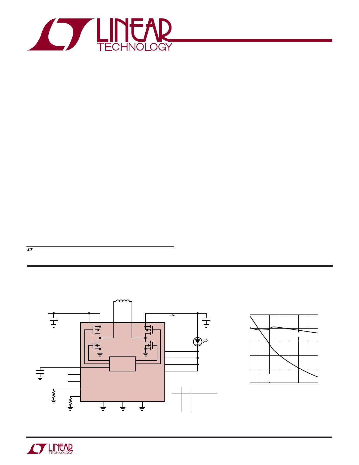
TYPICAL APPLICATIO
High Efficiency Torch/Flash LED Driver
V
IN
1-CELL
2.7V to 4.2V
0.1µF
Li-Ion
8.25k
2.2µF
EN1 (TORCH)
EN2 (FLASH)
1%
3.48k
1%
I
I
SET1
SET2
EN1
EN2
V
PV
IN
IN
V
C
U
L1
4.7µH
SW1 SW2 V
1MHz
BUCK-BOOST
GND PGNDGND
OUT
LTC3453
3453 TA01a
150mA/500mA
LED1
LED2
LED3
LED4
D1: LUMILEDS LXCL-PWF1
L1: VISHAY DALE IDCS-2512
EN1 EN2
0
0
1
0
0
1
1
1
D1
I
LED
0 (SHUTDOWN)
150mA
350mA
500mA
4.7µF
Torch Mode Efficiency vs V
100
(%)
IN
90
/P
LED
80
70
60
LED POWER EFFICIENCY P
I
= 150mA
LED
= 25°C
T
A
50
3.1 3.5 3.9 5.54.3 5.1
2.7
VIN (V)
EFFICIENCY
I
IN
4.7
IN
3453 TA01b
180
160
INPUT CURRENT (mA)
140
120
100
80
3453fa
1
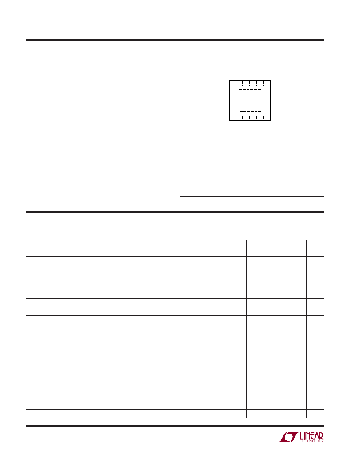
LTC3453
16 15 14 13
5 6 7 8
UF PACKAGE
16-LEAD (4mm × 4mm) PLASTIC QFN
9
10
11
17
12
4
3
2
1
TOP VIEW
V
IN
EN1
I
SET1
LED1
V
C
EN2
I
SET2
LED4
PVINSW1
SW2
V
OUT
GND
LED2
LED3
GND
WW
W
U
ABSOLUTE AXI U RATI GS
(Note 1)
VIN, PVIN, SW1, SW2, V
LED1 to LED4 Voltage ...... –0.3V to (V
, EN1, EN2,
V
C
I
, I
SET1
Voltage .......... –0.3V to (VIN + 0.3V) or 6V
SET2
LED1 to LED4 Peak Current ................................ 250mA
Storage Temperature Range ..................–65°C to 125°C
Operating Temperature Range (Note 2) ... –40°C to 85°C
Junction Temperature (Note 3).............................125°C
Voltage ............ –0.3V to 6V
OUT
+ 0.3V) or 6V
OUT
UUW
PACKAGE/ORDER I FOR ATIO
T
= 125°C, θJA = 40°C/W, θJC = 2.6°C/W
JMAX
EXPOSED PAD (PIN 17) IS PGND, MUST BE SOLDERED TO PCB
ORDER PART NUMBER
Order Options Tape and Reel: Add #TR
Lead Free: Add #PBF Lead Free Tape and Reel: Add #TRPBF
Lead Free Part Marking: http://www.linear.com/leadfree/
Consult LTC Marketing for parts specified with wider operating temperature ranges.
UF PART MARKING
3453LTC3453EUF
ELECTRICAL CHARACTERISTICS
temperature range, otherwise specifications are at T
PARAMETER CONDITIONS MIN TYP MAX UNITS
Input Supply Voltage
Input DC Supply Current
Normal Operation 2.7V ≤ V
Shutdown 2.7V ≤ V
UVLO V
Undervoltage Lockout Threshold VIN Rising
EN1,2 DC Threshold for Normal Operation 2.7V ≤ VIN ≤ 5.5V, V
EN1,2 DC Threshold for Shutdown (I
EN1,2 Input Current V
I
Servo Voltage R
SET1,2
LED Output Current Ratio I
LED Output Current Matching (MAX – MIN)/[(MAX + MIN)/2] • 100%, I
LED Pin Drain Voltage I
Regulated Maximum V
PMOS Switch R
NMOS Switch R
Forward Current Limit Switch A 1125 1612 2100 mA
Reverse Current Limit Switch D 200 mA
ON
ON
OUT
LEDx
IN
V
IN
= 0) 2.7V ≤ VIN ≤ 5.5V, V
EN1,2
ISET1,2
R
ISET1,2
LED
2.7V ≤ V
V
LEDx
LEDx
V
LEDx
Switches A and D, @ 100mA 0.3 Ω
Switches B and C, @ 100mA 0.25 Ω
≤ 5.5V, R
IN
≤ 5.5V; V
IN
< UVLO Threshold 3 5 µA
Falling 1.6 1.9 V
= 3.6V
= 4.12k, 0°C ≤ TA ≤ 85°C 788 800 812 mV
= 4.12k, –40°C ≤ TA ≤ 85°C
/(I
+ I
SET1
≤ 5.5V
IN
= 300mV
= 75mA 130 mV
= 0V
The ● denotes the specifications which apply over the full operating
= 25°C, VIN = V
A
||R
ISET1
= V
EN1
Rising
EN1,2
Falling
EN1,2
), I
SET2
= 75mA, V
LEDx
= 3.6V unless otherwise noted. (Note 2)
OUT
●
2.7 5.5 V
= 51.1k, I
ISET2
= 0V 6 18 µA
EN2
LEDx
= 0 (Note 4) 0.6 1 mA
LEDx
●
●
●
0.2 0.63 V
●
–1 1 µA
●
780 800 812 mV
= 300mV, 365 384 403 mA/mA
●
357 384 403 mA/mA
= 75mA 2 6 %
LEDx
●
4.4 4.5 4.6 V
2 2.3 V
0.65 1 V
3453fa
2
LTC3453
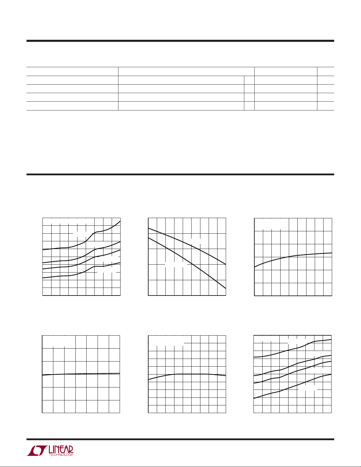
TEMPERATURE (°C)
–55
FREQUENCY (kHz)
1050
1040
1030
1020
950
1010
1000
990
980
970
960
45 65 85 10525
3453 G07
–35 –15 5 125
VIN = 5.5V
V
OUT
= 3V
VIN = 4.2V
VIN = 3.6V
VIN = 2.7V
ELECTRICAL CHARACTERISTICS
temperature range, otherwise specifications are at T
PARAMETER CONDITIONS MIN TYP MAX UNITS
PMOS Switch Leakage Switches A and D
NMOS Switch Leakage Switches B and C
Oscillator Frequency 0.9 1 1.1 MHz
Soft-Start Time 0.65 ms
Note 1: Stresses beyond those listed under Absolute Maximum Ratings
may cause permanent damage to the device. Exposure to any Absolute
Maximum Rating condition for extended periods may affect device
reliability and lifetime.
Note 2: The LTC3453E is guaranteed to meet specifications from 0°C to
70°C. Specifications over the –40°C to 85°C operating temperature range
are assured by design, characterization and correlation with statistical
process controls.
TYPICAL PERFOR A CE CHARACTERISTICS
Input DC Supply Current in
Shutdown vs Temperature
20
FRONT PAGE APPLICATION
18
16
14
12
10
(µA)
IN
I
8
6
4
2
0
–35 –15 5 125
–55
I
SET1,2
812
TA = 25°C
R
ISET1,2
808
804
(mV)
800
ISET1,2
V
796
792
788
2.7
Servo Voltage vs V
3.1 5.5
VIN = 5.5V
TEMPERATURE (°C)
= 8.25k
3.9 4.3 4.7 5.13.5
VIN (V)
VIN = 4.2V
45 65 85 10525
VIN = 3.6V
VIN = 2.7V
IN
UW
3453 G01
3453 G05
The ● denotes the specifications which apply over the full operating
= 25°C, VIN = V
A
= 3.6V unless otherwise noted. (Note 2)
OUT
Note 3: T
dissipation P
T
= TA + (PD • θJA °C/W).
J
Note 4: Dynamic supply current is higher due to the gate charge being
delivered at the switching frequency.
Undervoltage Lockout Threshold
vs Temperature
2.2
2.1
VIN RISING
2.0
1.9
UVLO THRESHOLD (V)
1.8
1.7
–55
VIN FALLING
–35 –15 5 125
TEMPERATURE (°C)
45 65 85 10525
Regulated Maximum V
Temperature
4.55
VIN = 3.6V
ALL LED PINS OPEN
4.54
4.53
4.52
4.51
(V)
4.50
OUT
V
4.49
4.48
4.47
4.46
4.45
–35 –15 5 125
–55
TEMPERATURE (°C)
45 65 85 10525
●
●
is calculated from the ambient temperature TA and power
J
according to the following formula:
D
I
Servo Voltage vs
SET1,2
Temperature
812
VIN = 3.6V
= 8.25k
R
ISET1,2
808
804
(mV)
800
ISET1,2
V
796
792
OUT
vs
3453 G02
788
–35 –15 5 125
–55
TEMPERATURE (°C)
Oscillator Frequency vs
45 65 85 10525
Temperature
3453 G06
1 µA
1 µA
3453 G04
3453fa
3
LTC3453
UW
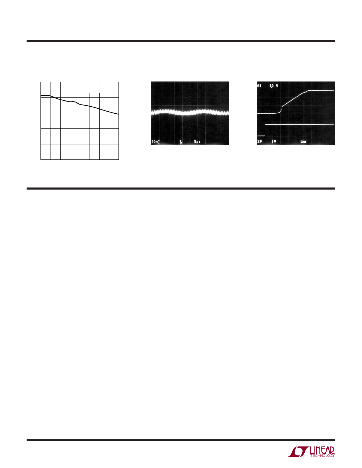
TYPICAL PERFOR A CE CHARACTERISTICS
Efficiency vs LED Current Output Voltage Ripple Startup Transient
100
90
FRONT PAGE APPLICATION
, VIN = 3.6V, TA = 25°C
P
LED/PIN
CH1, V
2V/DIV
OUT
80
70
EFFICIENCY (%)
60
50
150 200 250 500
100
LED CURRENT (mA)
350 400 450300
3453 G07
20mV/DIV
AC COUPLED
FRONT PAGE APPLICATION
= 3.6V
V
IN
= 150mA
I
LED
UUU
PI FU CTIO S
VIN (Pin 1): Signal Voltage Input Supply Pin [2.7V ≤ VIN ≤
5.5V]. Recommended bypass capacitor to GND is 2.2µF
ceramic or larger. Connect to PV
EN1 (Pin 2): Enable Input Pin for I
I
(Pin 3): White Led Current Programming Pin. A
SET1
resistor to ground programs each current source output to
I
= 384(0.8V/R
LED
any amount set by EN2/I
). This amount of current adds to
ISET1
SET2
LED1 to LED4 (Pins 4, 6, 7, 9): Individual Low Dropout
Current Source Outputs for White LED Current Biasing.
Connect each white LED between V
LEDx pin. Unused LEDx outputs should be connected to
.
V
OUT
GND (Pins 5 and 8): Signal Ground Pin. Connect to PGND
(Exposed Pad).
I
(Pin 10): White Led Current Programming Pin. A
SET2
resistor to ground programs each current source output to
I
= 384(0.8V/R
LED
any amount set by EN1/I
). This amount of current adds to
ISET2
SET1
(Pin 16).
IN
Current.
SET1
if also used.
and an individual
OUT
if also used.
0V
CH2, EN1
1V/DIV
0V
5µs/DIV
3453 G08
FRONT PAGE APPLICATION
= 3.6V
V
IN
= 150mA
I
LED
EN2 (Pin 11): Enable Input Pin for I
1ms/DIV
SET2
Current.
3453 G09
VC (Pin 12): Compensation Point for the Internal Error
Amplifier Output. Recommended compensation capacitor
to GND is 0.1µF ceramic or larger.
V
(Pin 13): Buck-Boost Output Pin. Recommended
OUT
bypass capacitor to GND is 4.7µF ceramic.
SW2 (Pin 14): Switching Node Pin. Connected to internal
power switches C and D. External inductor connects
between SW1 and SW2. Recommended value is 4.7µH.
SW1 (Pin 15): Switching Node Pin. Connected to internal
power switches A and B. External inductor connects
between SW1 and SW2. Recommended value is 4.7µH.
(Pin 16): Power Voltage Input Supply Pin. Connect to
PV
IN
V
(Pin 1).
IN
Exposed Pad (Pin 17): Power Ground Pin. Connect to
GND (Pin 8) and solder to PCB ground for optimum
thermal performance.
4
3453fa
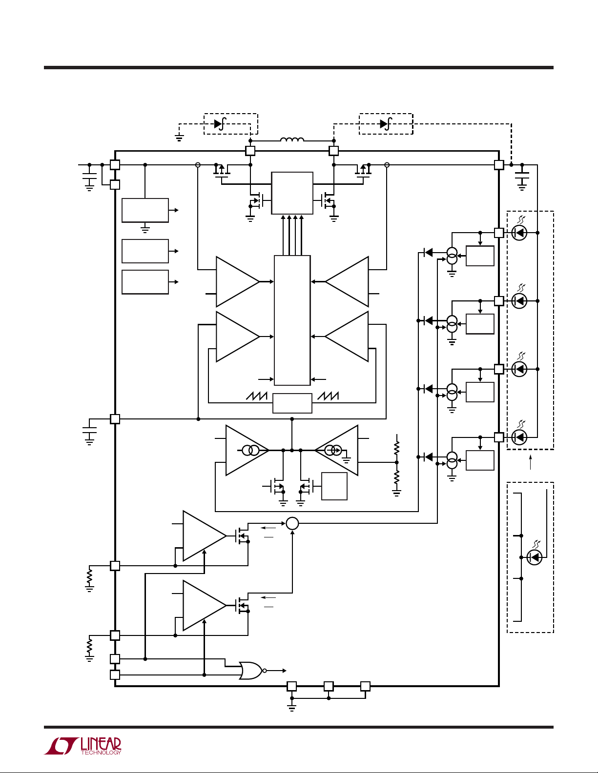
BLOCK DIAGRA
LTC3453
W
V
2.7V TO 5.5V
OPTIONAL
15 14
LIMIT
SW1
DRIVERS
ANTICROSS-
CONDUCTION
PV
IN
IN
16
V
IN
1
UNDERVOLTAGE
LOCKOUT
OVERTEMP
PROTECTION
SWITCH A
UV
OT
SWITCH B SWITCH C
FORWARD
CURRENT
+
BANDGAP
REFERENCE
1.23V
1612mA 200mA
–
+
LOGIC
–
AB PWM
COMPARATOR
UV
MAIN
ERROR AMP
OSCILLATOR
V
C
12
V
LED CURRENT
SETTING AMP 1
BIAS
V
–
FB
+
1.23V
GATE
AND
1MHz
SW2
COMPARATOR
SAFETY
ERROR AMP
START
CLAMP
REVERSE
CURRENT
LIMIT
CD PWM
OT
SOFT
SWITCH D
+
–
+
–
–
+
1.23V
OPTIONAL
V
OUT
LED1
LED
DETECT
LED2
LED
DETECT
LED3
LED
DETECT
V
OUT
327k
123k
LED4
LED
DETECT
V
13
4
6
7
9
OUT
OR
4
R
R
ISET1
ISET2
800mV
+
–
I
SET1
3
LED CURRENT
800mV
+
SETTING AMP 2
–
I
SET2
10
EN1
2
EN2
11
I
384
I
384
LED
LED
∑
SHUTDOWN
GND
5
6
7
9
GND
8
EXPOSED PAD (PGND)
17
3453 BD
3453fa
5

LTC3453
OPERATIO
U
Buck-Boost DC-DC Converter
The LTC3453 employs an LTC proprietary buck-boost
DC/DC converter to generate the output voltage required
to drive the LEDs. This architecture permits high-efficiency, low noise operation at input voltages above, below
or equal to the output voltage by properly phasing four
internal power switches. The error amp output voltage on
the V
pin determines the duty cycle of the switches. Since
C
the V
pin is a filtered signal, it provides rejection of
C
frequencies well below the factory trimmed switching
frequency of 1MHz. The low R
, low gate charge
DS(ON)
synchronous switches provide high frequency pulse width
modulation control at high efficiency. Schottky diodes
across synchronous rectifier switch B and synchronous
rectifier switch D are not required, but if used do provide
a lower voltage drop during the break-before-make time
(typically 20ns), which improves peak efficiency by typically 1% to 2% at higher loads.
Figure 1 shows a simplified diagram of how the four
internal power switches are connected to the inductor,
VIN, V
and GND. Figure 2 shows the regions of opera-
OUT
tion of the buck-boost as a function of the control voltage
V
. The output switches are properly phased so transi-
C
tions between regions of operation are continuous, filtered and transparent to the user. When V
V
, the buck-boost region is reached where the conduc-
OUT
approaches
IN
tion time of the four switch region is typically 150ns.
Referring to Figures 1 and 2, the various regions of
operation encountered as VC increases will now be
described.
Buck Mode (V
IN
> V
OUT
)
In buck mode, switch D is always on and switch C is always
off. Referring to Figure 2, when the control voltage V
is
C
above voltage V1, switch A begins to turn on each cycle.
During the off time of switch A, synchronous rectifier
switch B turns on for the remainder of the cycle. Switches
A and B will alternate conducting similar to a typical
synchronous buck regulator. As the control voltage increases, the duty cycle of switch A increases until the
maximum duty cycle of the converter in buck mode
reaches DC
DC
BUCK
where DC
|max given by:
BUCK
|max = 100% – DC
equals the duty cycle in % of the “four
4SW
4SW
switch” range.
DC
= (150ns • f) • 100%
4SW
where f is the operating frequency in Hz.
Beyond this point the “four switch” or buck-boost region
is reached.
Buck-Boost or Four-Switch Mode (V
IN
≈ V
Referring to Figure 2, when the control voltage V
OUT
)
is above
C
voltage V2, switch pair AD continue to operate for duty
cycle DC
|max, and the switch pair AC begins to phase
BUCK
in. As switch pair AC phases in, switch pair BD phases out
accordingly. When the V
voltage reaches the edge of the
C
buck-boost range at voltage V3, switch pair AC completely
phases out switch pair BD and the boost region begins at
75%
D
MAX
BOOST
PV
IN
16
PMOS A
SW1
15
NMOS B
Figure 1. Simplified Diagram of Internal Power Switches Figure 2. Switch Control vs Control Voltage, V
SW2
14
V
OUT
13
PMOS D
NMOS C
3453 F01
D
MIN
BOOST
D
MAX
BUCK
DUTY
CYCLE
A ON, B OFF
PWM CD SWITCHES
FOUR SWITCH PWM
D ON, C OFF
PWM AB SWITCHES
0%
BOOST REGION
BUCK/BOOST REGION
BUCK REGION
6
3453 F02
V4 (≈2.1V)
V3 (≈1.65V)
V2 (≈1.55V)
V1 (≈0.9V)
CONTROL
VOLTAGE, V
C
C
3453fa

OPERATIO
LTC3453
U
duty cycle DC
. The input voltage VIN where the four
4SW
switch region begins is given by:
V
= V
IN
and the input voltage V
/[1 – (150ns • f)]
OUT
where the four switch region
IN
ends is given by
V
= V
IN
Boost Mode (V
• (1 – DC
OUT
IN
< V
OUT
4SW
)
) = V
• [1 – (150ns • f)]
OUT
In boost mode, switch A is always on and switch B is
always off. Referring to Figure 2, when the control voltage
V
is above voltage V3, switches C and D will alternate
C
conducting similar to a typical synchronous boost regulator. The maximum duty cycle of the converter is limited to
88% typical and is reached when VC is above V4.
Forward Current Limit
If the current delivered from V
through PMOS switch A
IN
exceeds 1612mA (typical), switch A is shut off immediately. Switches B and D are turned on for the remainder of
the cycle in order to safely discharge the forward inductor
current at the maximum rate possible.
Soft-Start
The LTC3453 includes an internally fixed soft-start which
is active when powering up or coming out of shutdown.
The soft-start works by clamping the voltage on the V
C
node and gradually releasing it such that it requires
0.65ms to linearly slew from 0.9V to 2.1V. This has the
effect of limiting the rate of duty cycle change as V
C
transitions from the buck region through the buck-boost
region into the boost region. Once the soft-start times out,
it can only be reset by entering shutdown, or by an
undervoltage or overtemperature condition.
Main Error Amp
The main error amplifier is a transconductance amplifier
with source and sink capability. The output of the main
error amplifier drives a capacitor to GND at the VC pin. This
capacitor sets the dominant pole for the regulation loop.
(See the Applications Information section for selecting the
capacitor value.) The error amp gets its feedback signal
from a proprietary circuit which monitors all 4 LED current
sources to determine which LED to close the regulation
loop on.
Reverse Current Limit
If the current delivered from V
backwards through
OUT
PMOS switch D exceeds 200mA (typical), switch D is shut
off immediately. Switches A and C are turned on for the
remainder of the cycle in order to safely discharge the
reverse inductor current at the maximum rate possible.
Undervoltage Lockout
To prevent operation of the power switches at high R
DS(ON)
,
an undervoltage lockout is incorporated on the LTC3453.
When the input supply voltage drops below approximately
1.9V, the four power switches and all control circuitry are
turned off except for the undervoltage block, which draws
only several microamperes.
Overtemperature Protection
If the junction temperature of the LTC3453 exceeds 130°C
for any reason, all four switches are shut off immediately.
The overtemperature protection circuit has a typical hysteresis of 11°C.
Safety Error Amp
The safety error amplifier is a transconductance amplifier
with sink only capability. In normal operation, it has no
effect on the loop regulation. However, if any of the LED
pins open-circuits, the output voltage will keep rising, and
safety error amp will eventually take over control of the
regulation loop to prevent V
runaway. The V
OUT
OUT
thresh-
old at which this occurs is approximately 4.5V.
LED Current Setting Amplifiers and Enable Circuit
The LTC3453 includes two LED current setting amplifiers
that work in conjunction with dual external current setting
resistors and dual enable pins to program LED current to
one of four levels (including shutdown). All four LED
current source outputs are programmed to the same level.
When both enable inputs are logic low, the LTC3453 is in
shutdown, the buck-boost is disabled and all LED currents
are zero. In shutdown, the input supply current is typically
6µA. If either enable input is logic high, the buck-boost will
regulate the output voltage such that the LEDs are biased
3453fa
7

LTC3453
OPERATIO
U
at the current programmed by resistors R
R
. Individually enabled, each LED current setting
ISET2
ISET1
and/or
amplifier programs the output LED current to
= 384 (0.8V/R
I
LED
ISET1,2
)
If both enable inputs are logic high, the setting currents are
summed internally and the output LED current will be
given by
I
= 384 [0.8V/(R
LED
ISET1
|| R
ISET2
) ]
Thus three different (nonzero) current levels are programmable, optimal for low current LED torch and high current
LED camera flash applications.
LED Current Sources
Each LED pin is driven by a current source specifically
designed for low dropout. The LTC3453 employs a propri-
U
WUU
APPLICATIO S I FOR ATIO
etary architecture that determines which of the four LEDs
requires the largest forward voltage drop at its programmed current, and then generates a feedback voltage
based on this one for closing the buck-boost regulation
loop. This results in the lowest output voltage required for
regulating all of the LEDs and thus the highest LED power
efficiency. The voltage present at the LED pin of the
“controlling LED” will be typically 130mV at 75mA of
current.
LED Detect Circuit
If fewer than four LED outputs are required, unused ones
should be connected to V
. Each LED pin has an internal
OUT
LED detect circuit that disables the output current source
to save power if an output is not needed. A small 30µA
current is employed to detect the presence of an LED at
startup.
Component Selection
Inductor Selection
The high frequency operation of the LTC3453 allows the
use of small surface mount inductors. The inductor current ripple is typically set to 20% to 40% of the maximum
inductor current. For a given ripple the inductance terms
are given as follows:
VVV
L
>
VV V
L
>
f I Ripple V
2
•– •%
IN MIN OUT IN MIN
() ()
f I Ripple V
••%•
OUT IN MAX OUT
••%•
OUT MAX IN MAX
()
OUT MAX OUT
()
•–•%
()
()
() ()
100
100
,
2
where f = operating frequency, Hz
%Ripple = allowable inductor current ripple, %
V
V
= minimum input voltage, V
IN(MIN)
IN(MAX)
= maximum input voltage, V
For high efficiency, choose an inductor with a high frequency core material, such as ferrite, to reduce core loses.
The inductor should have low ESR (equivalent series
resistance) to reduce the I2R losses, and must be able to
handle the peak inductor current without saturating. Molded
chokes or chip inductors usually do not have enough core
to support peak inductor currents >1A. To minimize radiated noise, use a toroid, pot core or shielded bobbin
inductor. For the white LED application, a 4.7µH inductor
value is recommended. See Table 1 for a list of component
suppliers.
Table 1. Inductor Vendor Information
SUPPLIER WEB SITE
Coilcraft www.coilcraft.com
Cooper/Coiltronics www.cooperet.com
Murata www.murata.com
Sumida www.japanlink.com/sumida
Vishay-Dale www.vishay.com
V
= output voltage, V
OUT
I
OUT(MAX)
= maximum output load current
8
3453fa

LTC3453
U
WUU
APPLICATIO S I FOR ATIO
Input Capacitor Selection
Since the V
recommended to place at least a 2.2µF, low ESR bypass
capacitor to ground. See Table 2 for a list of component
suppliers.
Table 2. Capacitor Vendor Information
SUPPLIER WEB SITE
AVX www.avxcorp.com
Sanyo www.sanyovideo.com
Taiyo Yuden www.t-yuden.com
TDK www.component.tdk.com
Output Capacitor Selection
The bulk value of the capacitor is set to reduce the ripple
due to charge into the capacitor each cycle. The steady
state ripple due to charge is given by:
%_
Ripple Boost
Ripple Buck
%_
pin is the supply voltage for the IC it is
IN
IVV
OUT MAX OUT IN MIN
=
VV
()
IN MAX OUT
=
8
••••
VfLC
IN MAX OUT
•– •
() ()
()
()
CCV f
OUT OUT
–•
()
2
2
••
1100
%
100
%
Optional Schottky Diodes
Schottky diodes across the synchronous switches B and
D are not required, but provide a lower drop during the
break-before-make time (typically 20ns) of the NMOS to
PMOS transition, improving efficiency. Use a Schottky
diode such as an MBRM120T3 or equivalent. Do not use
ordinary rectifier diodes, since the slow recovery times
will compromise efficiency.
Closing the Feedback Loop
The LTC3453 incorporates voltage mode PWM control.
The control to output gain varies with operation region
(Buck, Boost, Buck/Boost), but is usually no greater than
15. The output filter exhibits a double pole response
given by:
f
FILTER POLE
where C
=
_
is the output filter capacitor.
OUT
2
1
•• •
π
LC
Hz
OUT
The output filter zero is given by:
f
FILTER ZERO
_
=
•• •
2
1
RC
π
ESR OUT
Hz
where C
= output filter capacitor, F
OUT
The output capacitance is usually many times larger in
order to handle the transient response of the converter.
For a rule of thumb, the ratio of the operating frequency to
the unity-gain bandwidth of the converter is the amount
the output capacitance will have to increase from the
above calculations in order to maintain the desired transient response.
The other component of ripple is due to the ESR (equivalent series resistance) of the output capacitor. Low ESR
capacitors should be used to minimize output voltage
ripple. For surface mount applications, Taiyo Yuden, TDK,
AVX ceramic capacitors, AVX TPS series tantalum capacitors or Sanyo POSCAP are recommended. For the white
LED application, a 4.7µF capacitor value is recommended.
See Table 2 for a list of component suppliers.
where R
is the capacitor equivalent series resistance.
ESR
A troublesome feature in Boost mode is the right-half
plane zero (RHP), and is given by:
2
V
f
RHPZ
=
2• • • •
IN
ILV
π
OUT OUT
Hz
The loop gain is typically rolled off before the RHP zero
frequency.
A simple Type I compensation network can be incorporated to stabilize the loop but at a cost of reduced bandwidth and slower transient response. To ensure proper
phase margin, the loop requires to be crossed over a
decade before the LC double pole.
3453fa
9

LTC3453
U
WUU
APPLICATIO S I FOR ATIO
The unity-gain frequency of the error amplifier with the
Type I compensation is given by:
g
f
=
UG
where gm is the error amp transconductance (typically
1/5.2k) and C
pin. For the white LED application, a 0.1µF or greater
V
C
capacitor value is recommended.
Paralleling LED Outputs for Higher Current
Two or more LED output pins can be connected together
in parallel to achieve higher output current in fewer than 4
LEDs. For a very high power LED such as a LumiLED, all
four outputs can be connected in parallel for maximum
total output current, as shown in the cover page application of this datasheet.
Maximum LED Current
As described in the Operation section, the output LED
current with both enable pins logic high is equal to
I
= 384 [0.8V/(R
LED
m
C
π2• •
VC
is the external capacitor to GND at the
VC
ISET1
|| R
ISET2
)]
Since the maximum continuous output current is limited
to 500mA, this sets a minimum limit on the parallel
combination of R
= (R
R
MIN
ISET1
ISET1
|| R
and R
ISET2)|MIN
equal to
ISET2
= 4(384[0.8V/500mA])
= 2458Ω
Although the LTC3453 can safely provide this current
continuously, the external LED(s) may not be rated for this
high a level of continuous current. Higher current levels
are generally reserved for pulsed applications, such as
LED camera flash. This is accomplished by programming
a high current with one of the R
resistors and pulsing
ISET
the appropriate enable pin.
Varying LED Brightness
Continuously variable LED brightness control can be
achieved by interfacing directly to one or both of the I
SET
pins. Figure 3 shows four such methods employing a
voltage DAC, a current DAC, a simple potentiometer or a
PWM input. It is not recommended to control brightness
by PWMing the enable pins directly as this will toggle the
LTC3453 in and out of shutdown and result in erratic
operation.
VOLTAGE
DAC
V
IN
ENx
LED1
LTC3453
I
LED4
SETx
R
≥ R
SET
MIN
V
DAC
(a)
V
IN
ENx
LED1
LTC3453
I
LED4
SETx
R
MIN
R
POT
(c)
V
OUT
0.8V – V
I
= 384
LED
I
= 384
LED
DAC
R
SET
CURRENT
V
OUT
0.8V
R
+ R
MIN
POT
DAC
R
100
V
IN
ENx
LED1
LTC3453
I
LED4
SETx
0.8V
IDAC ≤
R
MIN
V
IN
ENx
LED1
LTC3453
I
LED4
SETx
SET
R
≥ R
SET
MIN
V
PWM
1µF
f
≥ 5kHz
PWM
(b)
(d)
I
= 384 • IDAC
LED
I
= 384
LED
= 384
DV
V
OUT
V
OUT
0.8V – V
0.8V – (DC% • V
CC
PWM
R
SET
R
3453 F03
)
DVCC
SET
Figure 3. Brightness Control Methods: (a) Using Voltage DAC, (b) Using Current DAC, (c) Using Potentiometer, (d) Using PWM Input
3453fa
10

LTC3453
U
WUU
APPLICATIO S I FOR ATIO
Unused Outputs
If fewer than 4 LED pins are to be used, unused LEDx pins
should be connected to V
. The LTC3453 senses which
OUT
current source outputs are not being used and shuts off
the corresponding output currents to save power. A small
trickle current (~30µA) is still applied to unused outputs to
detect if a white LED is later switched in and also to
distinguish unused outputs from used outputs during
startup.
LED Failure Modes
If an individual LED fails as a short circuit, the current
source biasing it is shut off to save power. This is the same
U
PACKAGE DESCRIPTIO
UF Package
16-Lead Plastic QFN (4mm × 4mm)
(Reference LTC DWG # 05-08-1692)
operation as described previously (if the output were
initially designated unused at power-up by connecting its
LEDx pin to V
). Efficiency is not materially affected.
OUT
If an individual LED fails as an open circuit, the control loop
will initially attempt to regulate off of its current source
feedback signal, since it will appear to be the one requiring
the largest forward voltage drop to run at its programmed
current. This will drive V
LED will never accept its programmed current, V
higher. As the open circuited
OUT
OUT
must
be voltage-limited by means of a secondary control loop.
The LTC3453 limits V
to 4.5V in this failure mode. The
OUT
other LEDs will still remain biased at the correct programmed current but the overall circuit efficiency will
decrease.
4.35 ± 0.05
2.90 ± 0.05
0.72 ±0.05
2.15 ± 0.05
(4 SIDES)
PACKAGE OUTLINE
0.30 ±0.05
0.65 BSC
RECOMMENDED SOLDER PAD PITCH AND DIMENSIONS
4.00 ± 0.10
(4 SIDES)
PIN 1
TOP MARK
(NOTE 6)
NOTE:
1. DRAWING CONFORMS TO JEDEC PACKAGE OUTLINE MO-220 VARIATION (WGGC)
2. DRAWING NOT TO SCALE
3. ALL DIMENSIONS ARE IN MILLIMETERS
4. DIMENSIONS OF EXPOSED PAD ON BOTTOM OF PACKAGE DO NOT INCLUDE
MOLD FLASH. MOLD FLASH, IF PRESENT, SHALL NOT EXCEED 0.15mm ON ANY SIDE
5. EXPOSED PAD SHALL BE SOLDER PLATED
6. SHADED AREA IS ONLY A REFERENCE FOR PIN 1 LOCATION
ON THE TOP AND BOTTOM OF PACKAGE
0.75 ± 0.05
2.15 ± 0.10
(4-SIDES)
0.200 REF
0.00 – 0.05
BOTTOM VIEW—EXPOSED PAD
R = 0.115
TYP
1615
PIN 1 NOTCH R = 0.20 TYP
OR 0.35 × 45° CHAMFER
0.55 ± 0.20
1
2
(UF16) QFN 1004
0.30 ± 0.05
0.65 BSC
3453fa
Information furnished by Linear Technology Corporation is believed to be accurate and reliable.
However, no responsibility is assumed for its use. Linear Technology Corporation makes no representation that the interconnection of its circuits as described herein will not infringe on existing patent rights.
11

LTC3453
TYPICAL APPLICATIO
U
High Efficiency 4 White LED Driver
PV
IN
4.7µH
SW1
1MHz
BUCK-BOOST
GND
SW2 V
PGNDGND
OUT
LTC3453
3453 TA02
LED1
LED2
LED3
LED4
4.7µF 30mA2.2µF
D1 TO D4: NICHIA NSCW100
L1: VISHAY DALE IDCS-2512
30mA30mA30mA
V
1-CELL
Li-Ion
0.1µF
IN
10.2k
V
IN
V
C
EN1
EN
EN2
I
SET1
I
SET2
RELATED PARTS
PART NUMBER DESCRIPTION COMMENTS
LT1618 Constant Current, Constant Voltage 1.4MHz, High Efficiency VIN: 1.6V to 18V, V
Boost Regulator MS10 Package/EDD Package
LT1930/LT1930A 1A (ISW), 1.2MHz/2.2MHz, High Efficiency Step-Up VIN: 2.6V to 16V, V
DC/DC Converter ThinSOT Package
LT1932 Constant Current, 1.2MHz, High Efficiency White LED VIN: 1V to 10V, V
OUT(MAX)
Boost Regulator ThinSOT Package
LT1937 Constant Current, 1.2MHz, High Efficiency White LED VIN: 2.5V to 10V, V
Boost Regulator ThinSOT Package/SC70 Package
LTC3205 High Efficiency, Multi-Display LED Controller VIN: 2.8V to 4.5V, V
QFN-24 Package
LTC3216 1A Low Noise High Current LED Charge Pump with VIN: 2.9V to 4.4V, V
Independent Flash/Torch Current DFN Package
LTC3440/ 600mA/1.2A I
, 2MHz/1MHz, Synchronous Buck-Boost VIN: 2.4V to 5.5V, V
OUT
LTC3441 DC/DC Converter MS-10 Package/DFN Package
LTC3443 600mA/1.2A I
, 600kHz, Synchronous Buck-Boost VIN: 2.4V to 5.5V, V
OUT
DC/DC Converter DFN Package
LTC3454 1A Synchronous Buck-Boost High Power LED Driver VIN: 2.7V to 5.5V, 1MHz, ISD < 6µA, DFN Package
LT3465/LT3465A Constant Current, 1.2MHz/2.7MHz, High Efficiency White LED VIN: 2.7V to 16V, V
Boost Regulator with Integrated Schottky Diode ThinSOT Package
LT3466 Dual Constant Current, 2MHz, High Efficiency White LED VIN: 2.7V to 24V, V
Boost Regulator with Integrated Schottky Diode DFN Package
LT3479 3A, Full Featured DC/DC Converter with Soft-Start and VIN: 2.5V to 24V, V
Inrush Current Protection DFN Package/TSOPP Package
= 34V, IQ = 1.8mA, ISD = <1µA,
OUT(MAX)
= 34V, IQ = 4.2mA/5.5mA, ISD = <1µA,
OUT(MAX)
= 34V, IQ = 1.2mA, ISD = <1µA,
= 34V, IQ = 1.9mA, ISD = <1µA,
OUT(MAX)
= 6V, IQ = 50µA, ISD = <1µA,
OUT(MAX)
= 5.5V, IQ = 300µA, ISD = <2.5µA,
OUT(MAX)
= 5.25V, IQ = 25µA/50µA, ISD = <1µA,
OUT(MAX)
= 5.25V, IQ = 28µA, ISD = <1µA,
OUT(MAX)
= 34V, IQ = 1.9mA, ISD = <1µA,
OUT(MAX)
= 40V, IQ = 5mA, ISD = <16µA,
OUT(MAX)
= 40V, IQ = 6.5mA, ISD = <1µA,
OUT(MAX)
D4D3D2D1
12
Linear Technology Corporation
1630 McCarthy Blvd., Milpitas, CA 95035-7417
(408) 432-1900 ● FAX: (408) 434-0507
●
www.linear.com
3453fa
LT 0206 REV A • PRINTED IN USA
© LINEAR TECHNOLOGY CORPORATION 2005
 Loading...