

One IC Generates Three Sub-2V Power Rails from a Li-Ion Cell
.
Design Note 419
Frank Lee
Introduction
Shrinking geometries in IC technology have pushed the
operating voltages of today’s electronics well below 2V,
presenting a number of design challenges. One common
problem is the need for multiple supply voltages: for
example, one voltage for a CPU core, another for I/O and
still others for peripherals. Sensitive RF, audio and analog
circuitry may require additional dedicated quiet supplies,
separate from less noise-sensitive digital circuits. As the
number of supplies increases, it becomes impractical
to use a separate power supply IC for each voltage and
special-requirements subsystem. Board area would be
quickly consumed by power supplies. One solution to
the space crunch is power supply integration, provided
®
by a triple regulator like the LTC
3446—three voltages
from a single IC.
Triple Supply in a Tiny Package
The LTC3446 combines a 1A synchronous buck regula-
TM
tor with two 300mA very low dropout (VLDO
) linear
regulators to provide up to three stepped-down output voltages from a single input voltage, all in a tiny
3mm × 4mm DFN. The 2.7V to 5.5V input voltage range
is ideally suited for Li-Ion/Polymer battery-powered ap-
plications, and for powering low voltage logic from 5V
or 3.3V rails. The output voltage range extends down
to 0.4V for the VLDO regulators and 0.8V for the buck
converter.
Each output is independently enabled or shut down via
its own enable pin. When all outputs are shut down,
quiescent current drops to 1μA or less, conserving
V
IN
battery power. The regulation voltage for each output
is programmed by external resistor dividers. The buck
regulator loop response can be tailored to the load by
adjusting the RC network at the I
TH
pin.
High Effi ciency and Low Noise
The 1A synchronous buck provides the main output with
high effi ciency, up to 90%. This buck converter features
constant-frequency curren t-mode operation at 2.25MHz,
allowing small capacitors and inductor to be used. The
two 300mA VLDO regulators can be connected to run
off the buck output to provide two additional lower voltage outputs. This way, the buck performs the bulk of the
step-down at the high effi ciencies typical of switching
, LT, LTC and LTM are registered trademarks of Linear Technology Corporation.
Burst Mode and VLDO are registered trademarks of Linear Technology Corporation
All other trademarks are the property of their respective owners.
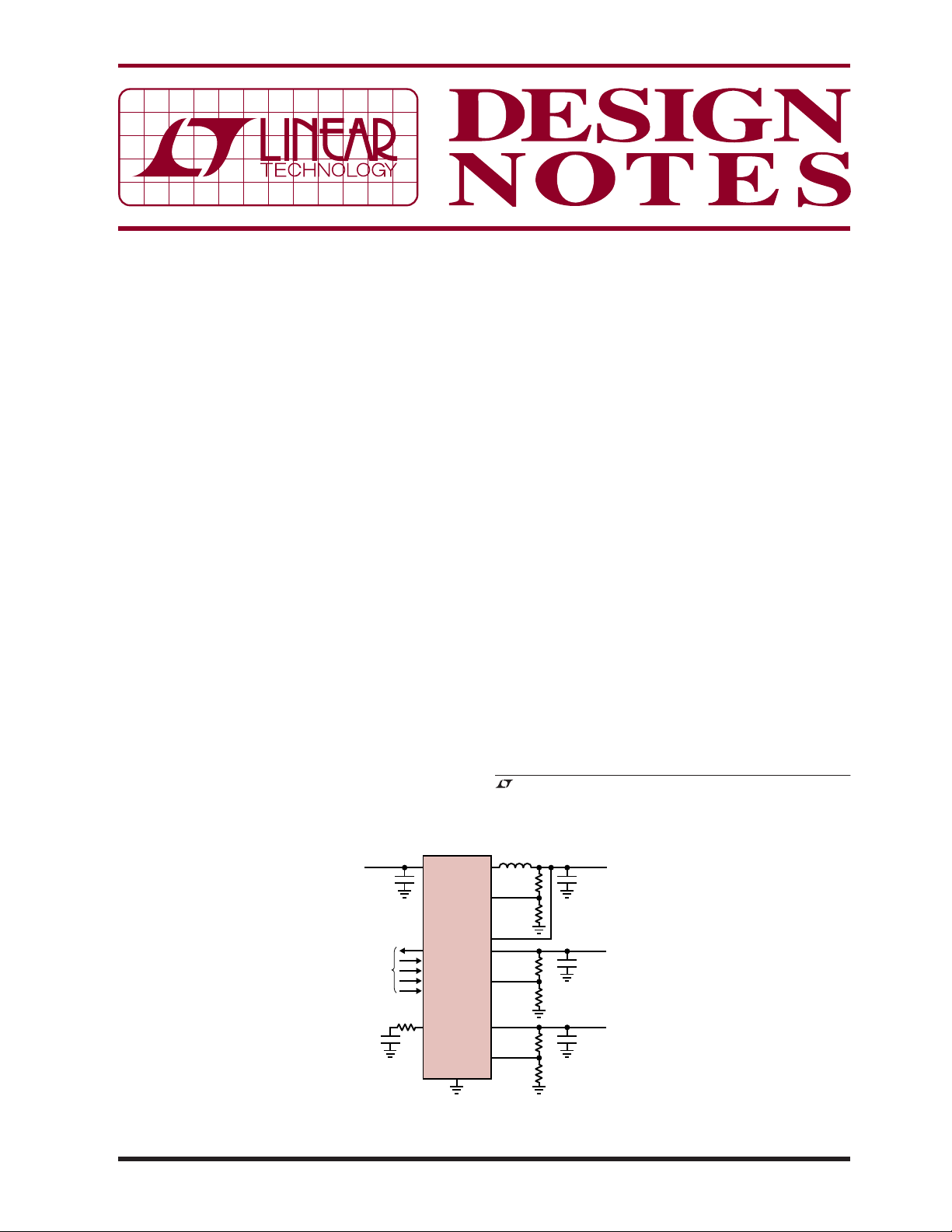
L1
2.9V TO 5.5V
V
IN
DIGITAL
CONTROL
1000pF
22μF
X7R
3.3k
V
IN
LTC3446
PGOOD
MODESEL
ENBUCK
ENLDO1
ENLDO2
I
TH
GND
BUCKFB
LV
LV
OUT1
LV
LV
OUT2
LV
DN419 F01
1.8μH
SW
59k
47.5k
IN
110k
FB1
40.2k
80.6k
FB2
40.2k
L1: TOKO A960AW-1R8M
22μF
X7R
2.2μF
X7R
2.2μF
X7R
V
OUT
1.8V
400mA MAX
V
OUT
1.5V
300mA MAX
V
OUT
1.2V
300mA MAX
Figure 1. Schematic Showing the LTC3446 Power Supply Confi gured to Deliver 1.8V from the 1A Buck, and 1.5V and
1.2V from the 300mA VLDO Regulators. The VLDO Regulators Are Powered from the Buck Output via the LVIN Pin.
07/07/419
regulators, while the VLDO regulators provide additional
lower voltages with good effi ciency at the extremely low
noise levels typical of linear regulators.
The schematic in Figure 1 shows the LTC3446 confi gured
to deliver 1.8V from the buck, 1.5V from the fi rst VLDO
regulator, and 1.2V from the second VLDO regulator.
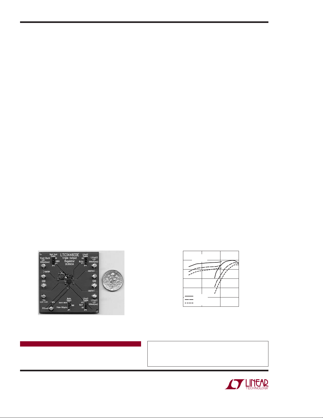
Figure 2 shows the Figure 1 circuit assembled onto a
printed-circuit board.
Selectable Burst Mode® Operation or PulseSkipping at Light Load
The LTC3446’s buck regulator f eatures Burst Mode operation for optimum effi ciency when operating at light loads,
at the cost of increased output ripple and the introduction
of switching noise below the 2.25MHz clock frequency.
Burst Mode operation can be defeated by bringing the
MODESEL pin high, which commands the LTC3446 to
continue to switch at the 2.25MHz clock frequency down
to very light loads, whereupon pulses are skipped as
needed to maintain regulation. Figure 3, which shows
the effi ciency of the buck regulator vs load current, also
illustrates the typical effi ciency gains from using Burst
Mode operation at load currents below 100mA.
Very Low Dropout (VLDO) Linear Regulators
The VLDOs in the LTC3446 employ an NMOS source-follower architecture to overcome the traditional tradeoff
between dropout voltage, quiescent current and load
transient response inherent in most PMOS- and PNPbased LDO regulator architectures. The V
pin (refer
IN
to Figure 1), supplies only the micropower bias needed
by the VLDO control and reference circuits, typically at
single-cell Li-Ion voltages. The actual load current is
sourced from the LV
pin, which can be connected to
IN
the buck regulator output.
Each VLDO regulator provides a high accuracy output
that is capable of supplying 300mA of output current
with a typical dropout voltage of only 70mV from LV
to LV
. VIN should exceed the LV
OUT
regulation point
OUT
IN
by 1.4V to provide suffi cient gate drive to the internal
NMOS pass device. Typical single-cell Li-Ion operating
voltages extend down to 3.2V, supporting VLDO output
voltages of up to 1.8V.
A single ceramic c apacitor between 1μF and 2.2μF is all tha t
is required for output bypassing. A low reference voltage
of 400mV allows the VLDO regulators to be programmed
to much lower voltages than are commonly available in
LDO regulators.
Power Good Detection
The LTC3446 includes a built-in supply monitor. The
PGOOD open-drain output pin is pulled low while any
enabled output is mor e than ±8% from its regula tion value.
Once all enabled outputs are within this tolerance window,
the PGOOD pin becomes high impedance. A microproc essor can monitor this open drain output pin to assess when
a recently enabled output has completed startup.
Conclusion
The LTC3446 packs an effi cient 1A buck regulator and
two 300mA VLDO regulators in a tiny 3mm × 4mm DFN
package. With an output voltage range extending down
to 0.4V for the VLDO regulators and 0.8V for the buck,
and an input voltage range covering the single-cell LiIon range up to 5.5V, the LTC3446 is ideal for powering
today’s multi-voltage, sub-2V systems.
100
Burst Mode
OPERATION
90
PWM
MODE
Figure 2. The LTC3446 Triple Power Supply
Assembled on a Printed Circuit Board
Data Sheet Download
www.linear.com
Linear Technology Corporation
1630 McCarthy Blvd., Milpitas, CA 95035-7417
(408) 432-1900
●
FAX: (408) 434-0507 ● www.linear.com
80
70
EFFICIENCY (%)
60
1
VIN = 2.7V
= 3.6V
V
IN
= 4.2V
V
IN
10 100
LOAD CURRENT (mA)
1000
DN419 F03
50
40
Figure 3. Effi ciency of the LTC3446’s
Buck Regulator vs Load
For applications help,
call (408) 432-1900, Ext. 2759
dn419f LT/TP 0707 409K • PRINTED IN THE USA
© LINEAR TECHNOLOGY CORPORATION 2007
 Loading...