

FEATURES
■
Regulated Output with Input Above, Below or Equal
to the Output
■
Single Inductor, No Schottky Diodes
■
High Efficiency: Up to 95%
■
25µA Quiescent Current in Burst Mode® Operation
■
Up to 1.2A Continuous Output Current from a Single
Lithium-Ion
■
True Output Disconnect in Shutdown
■
2.4V to 5.5V Input Range
■
2.4V to 5.25V Output Range
■
1MHz Fixed Frequency Operation
■
Synchronizable Oscillator
■
Selectable Burst Mode or Fixed Frequency Operation
■
<1µA Quiescent Current in Shutdown
■
Small, Thermally Enhanced 12-Lead (4mm × 3mm)
DFN package
U
APPLICATIO S
■
Handheld Computers
■
Handheld Instruments
■
MP3 Players
■
Digital Cameras
, LTC and LT are registered trademarks of Linear Technology Corporation.
Burst Mode is a registered trademark of Linear Technology Corporation.
LTC3441
High Current Micropower
Synchronous Buck-Boost
DC/DC Converter
U
DESCRIPTIO
The LTC®3441 is a high efficiency, fixed frequency, buckboost DC/DC converter that operates efficiently from input
voltages above, below or equal to the output voltage. The
topology incorporated in the IC provides a continuous transfer function through all operating modes, making the product ideal for single lithium ion or multicell applications where
the output voltage is within the battery voltage range.
The device includes two 0.10Ω N-channel MOSFET
switches and two 0.11Ω P-channel switches. External
Schottky diodes are optional, and can be used for a
moderate efficiency improvement. The operating frequency
is internally set to 1MHz and can be synchronized up to
1.7MHz. Quiescent current is only 25µA in Burst Mode
operation, maximizing battery life in portable applications.
Burst Mode operation is user controlled and can be
enabled by driving the MODE/SYNC pin high. If the MODE/
SYNC pin is driven low or with a clock, then fixed frequency switching is enabled.
Other features include a 1µA shutdown, soft-start control,
thermal shutdown and current limit. The LTC3441 is
available in a thermally enhanced 12-lead (4mm × 3mm)
DFN package.
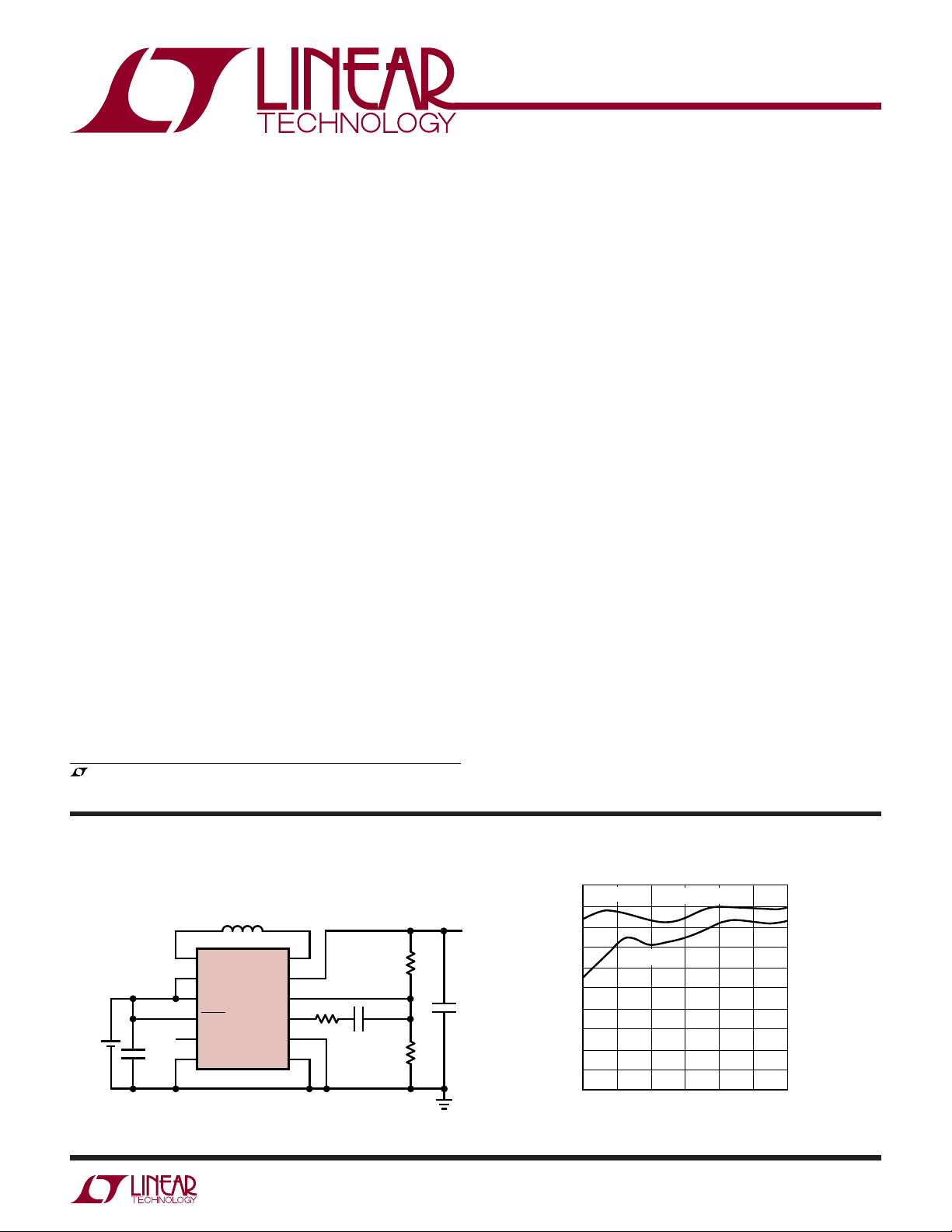
TYPICAL APPLICATIO
Li-Ion to 3.3V at 1A Buck-Boost Converter
L1
4.7µH
4
2.5V TO 4.2V
Li-Ion
*1 = Burst Mode OPERATION
0 = FIXED FREQUENCY
C
IN
10µF
*
SW1
9
PV
10
V
1
SHDN/SS
7
MODE/SYNC
3
PGND
IN
IN
SW2
V
OUT
LTC3441
FB
V
C
GND
PGND
: TAIYO YUDEN JMK212BJ106MG
C
IN
: TAIYO YUDEN JMK325BJ226MM
C
OUT
L1: TOKO A916CY-4R7M
U
Efficiency vs V
100
V
= 3.3V
OUT
V
OUT
3.3V
5
8
12
15k
11
2
6
1.5nF
340k
200k
1A
C
OUT
22µF
3441 TA01
95
90
85
80
75
70
EFFICIENCY (%)
65
60
55
50
2.5
I
= 1A
OUT
3
3.5
VIN (V)
I
= 200mA
OUT
4 4.5
IN
5.5
5
3441 TA02
sn3441 3441fs
1
LTC3441
PACKAGE/ORDER I FOR ATIO
UU
W
WWWU
ABSOLUTE AXI U RATI GS
(Note 1)
VIN, V
SW1, SW2 Voltage
DC ........................................................... – 0.3V to 6V
Pulsed < 100ns ...................................... –0.3V to 7V
SHDN/SS, MODE/SYNC Voltage ................. –0.3V to 6V
Operating Temperature Range (Note 2) .. – 40°C to 85°C
Maximum Junction Temperature (Note 4) ........... 125°C
Storage Temperature Range ................ –65°C to 125°C
Voltage........................................ –0.3V to 6V
OUT
TOP VIEW
13
= 125°C
12
FB
11
V
V
10
PV
9
V
8
MODE/SYNC
7
C
IN
IN
OUT
SHDN/SS
Consult LTC Marketing for parts specified with wider operating temperature ranges.
1
GND
2
PGND
3
SW1
4
SW2
5
PGND
6
12-LEAD (4mm × 3mm) PLASTIC DFN
DE12 PACKAGE
T
JMAX
= 53°C/W 1-LAYER BOARD
θ
JA
θ
= 43°C/W 4-LAYER BOARD
JA
= 4.3°C/W
θ
JC
EXPOSED PAD IS PGND (PIN 13)
MUST BE SOLDERED TO PCB
ORDER PART
NUMBER
LTC3441EDE
DE PART MARKING
3441
ELECTRICAL CHARACTERISTICS
temperature range, otherwise specifications are at TA = 25°C. VIN = V
PARAMETER CONDITIONS MIN TYP MAX UNITS
Input Start-Up Voltage ● 2.3 2.4 V
Output Voltage Adjust Range ● 2.4 5.25 V
Feedback Voltage ● 1.19 1.22 1.25 V
Feedback Input Current VFB = 1.22V 1 50 nA
Quiescent Current—Burst Mode Operation VC = 0V, MODE/SYNC = 3V (Note 3) 25 40 µA
Quiescent Current—SHDN V
Quiescent Current—Active MODE/SYNC = 0V (Note 3) 520 900 µA
NMOS Switch Leakage Switches B and C 0.1 7 µA
PMOS Switch Leakage Switches A and D 0.1 10 µA
NMOS Switch On Resistance Switches B and C 0.10 Ω
PMOS Switch On Resistance Switches A and D 0.11 Ω
Input Current Limit ● 2 3.2 A
Max Duty Cycle Boost (% Switch C On) ● 70 88 %
Min Duty Cycle ● 0%
Frequency Accuracy ● 0.85 1 1.15 MHz
MODE/SYNC Threshold ● 0.4 1.4 V
MODE/SYNC Input Current V
Error Amp AV
Error Amp Source Current 14 µA
Error Amp Sink Current 300 µA
SHDN/SS Threshold When IC is Enabled ● 0.4 1 1.4 V
SHDN/SS Threshold When EA is at Max Boost Duty Cycle 2 2.4 V
SHDN/SS Input Current V
OL
= SHDN = 0V, Not Including Switch Leakage 0.1 1 µA
OUT
Buck (% Switch A In)
MODE/SYNC
SHDN
= 5.5V 0.01 1 µA
= 5.5V 0.01 1 µA
The ● denotes the specifications which apply over the full operating
= 3.6V,unless otherwise noted.
OUT
● 100 %
90 dB
sn3441 3441fs
2
ELECTRICAL CHARACTERISTICS
LTC3441
Note 1: Absolute Maximum Ratings are those values beyond which the life
of a device may be impaired.
Note 2: The LTC3441E is guaranteed to meet performance specifications
from 0°C to 70°C. Specifications over the –40°C to 85°C operating
temperature range are assured by design, characterization and correlation
Note 4: This IC includes overtemperature protection that is intended to
protect the device during momentary overload conditions. Junction
temperature will exceed 125°C when overtemperature protection is active.
Continuous operation above the specified maximum operating junction
temperature may result in device degradation or failure.
with statistical process controls.
Note 3: Current measurements are preformed when the outputs are not
switching.
UW
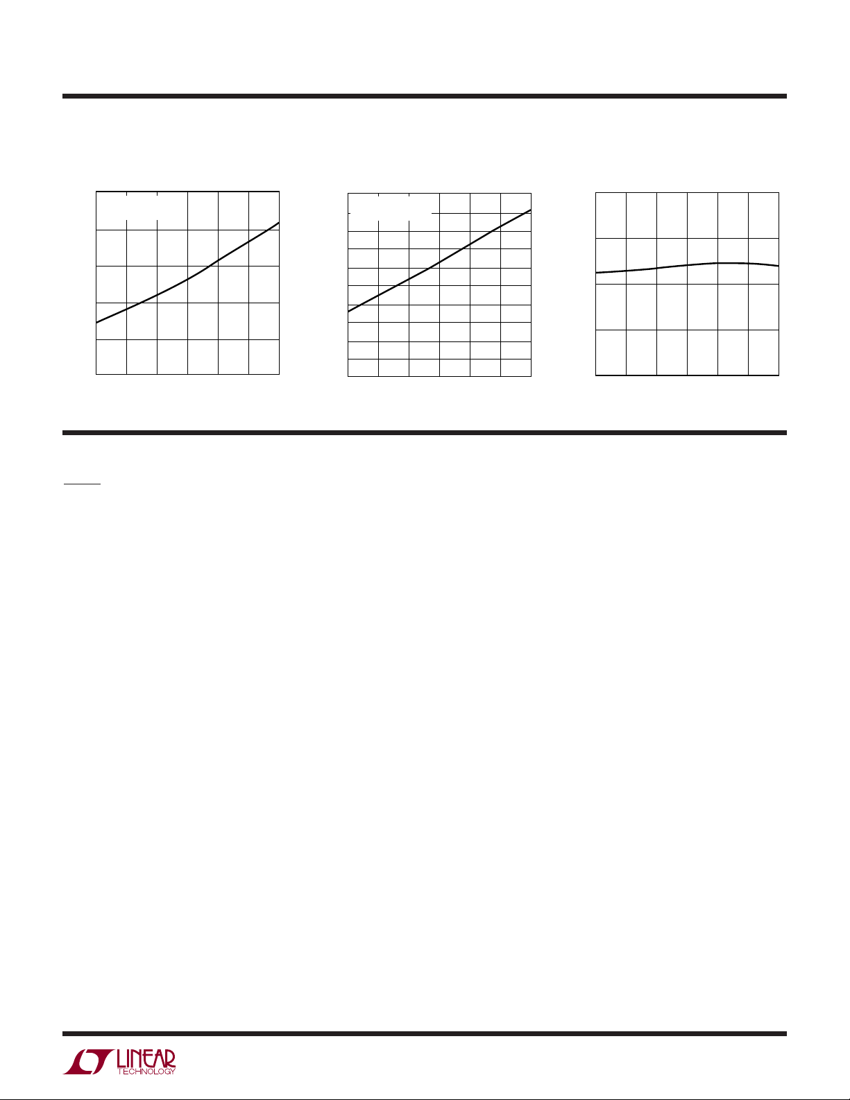
TYPICAL PERFOR A CE CHARACTERISTICS
Efficiency
100
90
Burst Mode
OPERATION
80
70
60
50
VIN = 2.7V
40
EFFICIENCY (%)
30
20
10
V
= 3.3V
OUT
0
0.1 10 100 1000
1
I
OUT
VIN = 4.2V
VIN = 3.6V
(mA)
3441 G17
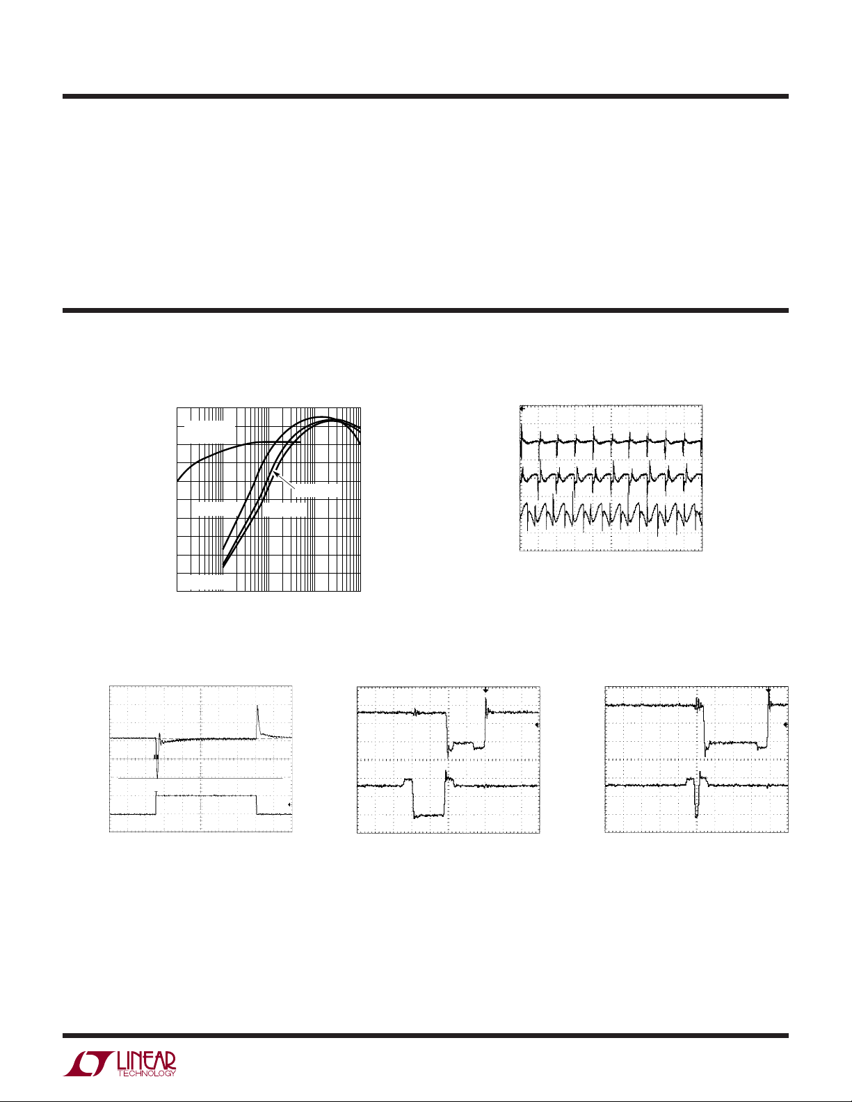
10mV/DIV
AC-COUPLED
V
Ripple at 1A Load
OUT
V
OUT
L = 4.7µH1µs/DIV
C
= 47µF
OUT
I
= 1A
OUT
= 3.3V
V
OUT
3441 G02
BUCK
VIN = 4.2V
BUCK-BOOST
V
= 3.3V
IN
BOOST
V
= 2.7V
IN
V
OUT
100mV/DIV
1A
100mA
Load Transient Response,
100mA to 1A
100µs/DIV
3441 G01
Switch Pins in Buck-Boost Mode
SW1
2V/DIV
SW2
2V/DIV
V
= 3.3V 50ns/DIV 3441 G03
IN
V
= 3.3V
OUT
I
= 500mA
OUT
Switch Pins Entering
Buck-Boost Mode
SW1
2V/DIV
SW2
2V/DIV
V
= 4.2V 50ns/DIV 3441 G04
IN
V
= 3.3V
OUT
I
= 500mA
OUT
sn3441 3441fs
3
LTC3441
TEMPERATURE (°C)
–55
2.8
CURRENT LIMIT (A)
3.0
3.2
3.4
–25 5 35 65
3441 G13
95
125
VIN = V
OUT
= 3.6V
UW
TYPICAL PERFOR A CE CHARACTERISTICS
Switch Pins Before Entering
Active Quiescent Current
630
CURRENT (µA)
OUT
+ V
IN
V
620
610
600
590
580
570
560
550
540
530
520
VIN = V
–55
= 3.6V
OUT
–25 5 35 65
TEMPERATURE (°C)
95 125
SW1
2V/DIV
SW2
2V/DIV
Boost Mode
= 3V 50ns/DIV 3441 G05
V
IN
V
= 3.3V
OUT
= 500mA
I
OUT
3441 G06
Feedback Voltage
1.241
VIN = V
= 3.6V
–55
OUT
–25
TEMPERATURE (°C)
1.236
1.231
1.226
1.221
1.216
1.211
FEEDBACK VOLTAGE (V)
1.206
1.201
1.196
5
35 125
65
95
3441 G07
Burst Mode Quiescent Current
50
CURRENT (µA)
OUT
+ V
IN
V
VIN = V
40
30
20
10
–55
= 3.6V
OUT
–25 5 35 65
TEMPERATURE (°C)
Error Amp Sink Current
400
VIN = V
350
300
OUT
= 3.6V
95 125
3441 G08
Feedback Voltage Line Regulation Error Amp Source Current
90
VIN = V
80
70
LINE REGULATION (dB)
60
–55
= 2.4V TO 5.5V
OUT
–25 5 35 65
TEMPERATURE (°C)
125
95
3441 G09
20
VIN = V
= 3.6V
OUT
15
10
EA SOURCE CURRENT (µA)
5
–55
–25 5 35 65
TEMPERATURE (°C)
Output Frequency Current Limit
1.2
VIN = V
1.1
1.0
OUT
= 3.6V
125
95
3441 G10
EA SINK CURRENT (µA)
250
200
4
–55
–25 5 35 65
TEMPERATURE (°C)
95 125
3441 G11
FREQUENCY (MHz)
0.9
0.8
–55
–25 5 35 65
TEMPERATURE (°C)
95 125
3441 G12
sn3441 3441fs
UW
TEMPERATURE (°C)
–55
2.10
MINIMUM START VOLTAGE (V)
2.15
2.20
2.25
2.30
–25 5 35 65
3441 G16
95 125
TYPICAL PERFOR A CE CHARACTERISTICS
LTC3441
NMOS R
0.15
VIN = V
SWITCHES B AND C
0.13
(Ω)
0.11
DS(ON)
0.09
NMOS R
0.07
0.05
–55
U
DS(ON)
= 3.6V
OUT
53565
–25
TEMPERATURE (°C)
95 125
3441 G14
UU
0.15
0.14
0.13
0.12
(Ω)
0.11
0.10
DS(ON)
0.09
PMOS R
0.08
0.07
0.06
0.05
PMOS R
–50
DS(ON)
VIN = V
SWITCHES A AND D
= 3.6V
OUT
–25
5
TEMPERATURE (°C)
PI FU CTIO S
SHDN/SS (Pin 1): Combined Soft-Start and Shutdown.
Applied voltage < 0.4V shuts down the IC. Tie to >1.4V to
enable the IC and >2.4V to ensure the error amp is not
clamped from soft-start. An RC from the shutdown command signal to this pin will provide a soft-start function by
limiting the rise time of the VC pin.
GND (Pin 2): Signal Ground for the IC.
PGND (Pins 3, 6, 13 Exposed Pad): Power Ground for the
Internal NMOS Power Switches
Minimum Start Voltage
35 65
125
95
3441 G15
light loads. The Burst Mode operation will continue until
the pin is driven low.
MODE/SYNC = Low: Disable Burst Mode operation and
maintain low noise, constant frequency operation .
MODE/SYNC = External CLK : Synchronization of the
internal oscillator and Burst Mode operation disable. A
clock pulse width between 100ns and 2µs and a clock
frequency between 2.3MHz and 3.4MHz (twice the
desired frequency) is required to synchronize the IC.
SW1 (Pin 4): Switch pin where the internal switches A and
B are connected. Connect inductor from SW1 to SW2. An
optional Schottky diode can be connected from this SW1
to ground. Minimize trace length to keep EMI down.
SW2 (Pin 5): Switch pin where the internal switches C
and D are connected. An optional Schottky diode can be
connected from SW2 to V
V
> 4.3V). Minimize trace length to keep EMI down.
OUT
MODE/SYNC (Pin 7): Burst Mode Select and Oscillator
Synchronization.
MODE/SYNC = High: Enable Burst Mode Operation.
During the period where the IC is supplying energy to
the output, the inductor peak inductor current will reach
0.8A and return to zero current on each cycle. In Burst
Mode operation the operation is variable frequency,
which provides a significant efficiency improvement at
(it is required where
OUT
f
= f
OSC
V
(Pin 8): Output of the Synchronous Rectifier. A filter
OUT
capacitor is placed from V
capacitor is recommended as close to the V
SYNC
/2
to GND. A ceramic bypass
OUT
and GND
OUT
pins as possible.
PVIN (Pin 9): Power VIN Supply Pin. A 10µF ceramic capaci-
tor is recommended as close to the PVIN and PGND pins
as possible
VIN (Pin 10): Input Supply Pin. Internal VCC for the IC.
VC (Pin 11): Error Amp Output. A frequency compensation
network is connected from this pin to the FB pin to
compensate the loop. See the section “Compensating the
Feedback Loop” for guidelines.
FB (Pin 12): Feedback Pin. Connect resistor divider tap
here. The output voltage can be adjusted from 2.4V to
5.25V. The feedback reference voltage is typically 1.22V.
sn3441 3441fs
5

LTC3441
BLOCK DIAGRA
W
2.4V TO 5.5V
+
V
IN
PV
IN
9
V
IN
10
SW A
3.2A
+
4A
–
V
CC
INTERNAL
+
2.4V
–
4 5
SW1
SW B
ANTICROSS
CONDUCTION
+
1
= k
g
m
100
–
AVERAGE
CURRENT LIMIT
SUPPLY
CURRENT
LIMIT
UVLO
GATE
DRIVERS
AND
PWM
LOGIC
AND
OUTPUT
PHASING
SW2
SW C
I
SENSE
AMP
PGND
THERMAL
SHUTDOWN
PWM
COMPARATORS
–0.8A
–
–
+
–
+
SW D
+
REVERSE
CURRENT
LIMIT
ERROR
AMP
CLAMP
V
OUT
8
1.22V
+
FB
–
12
V
OUT
2.4V TO 5.25V
R1
MODE/SYNC
7
1 = Burst Mode
OPERATION
0 = FIXED FREQUENCY
1MHz
OSC
SYNC
÷2
SLEEP
Burst Mode
OPERATION
CONTROL
5µs DELAY
GND
2
V
C
11
R2
R
SHUTDOWN
PGND
6
SHDN/SS
SS
1
V
IN
C
SS
3440 BD
6
sn3441 3441fs

OPERATIO
75%
D
MAX
BOOST
D
MIN
BOOST
D
MAX
BUCK
DUTY
CYCLE
0%
V4 (≈2.05V)
V3 (≈1.65V)
BOOST REGION
BUCK REGION
BUCK/BOOST REGION
V2 (≈1.55V)
V1 (≈0.9V)
3441 F02
A ON, B OFF
PWM CD SWITCHES
D ON, C OFF
PWM AB SWITCHES
FOUR SWITCH PWM
INTERNAL
CONTROL
VOLTAGE, V
CI
LTC3441
U
The LTC3441 provides high efficiency, low noise power for
applications such as portable instrumentation. The LTC
proprietary topology allows input voltages above, below or
equal to the output voltage by properly phasing the output
switches. The error amp output voltage on the VC pin determines the output duty cycle of the switches. Since the
VC pin is a filtered signal, it provides rejection of frequencies from well below the switching frequency. The low
R
, low gate charge synchronous switches provide
DS(ON)
high frequency pulse width modulation control at high
efficiency. Schottky diodes across the synchronous switch
D and synchronous switch B are not required, but provide
a lower drop during the break-before-make time (typically
15ns). The addition of the Schottky diodes will improve peak
efficiency by typically 1% to 2%. High efficiency is achieved
at light loads when Burst Mode operation is entered and
when the IC’s quiescent current is a low 25µA.
LOW NOISE FIXED FREQUENCY OPERATION
Oscillator
The frequency of operation is factory trimmed to 1MHz.
The oscillator can be synchronized with an external clock
applied to the MODE/SYNC pin. A clock frequency of twice
the desired switching frequency and with a pulse width of
at least 100ns is applied. The oscillator sync range is
1.15MHz to 1.7MHz (2.3MHz to 3.4MHz sync frequency).
Error Amp
The error amplifier is a voltage mode amplifier. The loop
compensation components are configured around the
amplifier to obtain stability of the converter. The SHDN/SS
pin will clamp the error amp output, V
, to provide a soft-
C
start function.
Reverse Current Limit
The reverse current limit amplifier monitors the inductor
current from the output through switch D. Once a negative
inductor current exceeds –800mA typical, the IC will shut
off switch D.
Output Switch Control
Figure 1 shows a simplified diagram of how the four
internal switches are connected to the inductor, VIN, V
OUT
and GND. Figure 2 shows the regions of operation for the
LTC3441 as a function of the internal control voltage, V
.
CI
The VCI voltage is a level shifted voltage from the output of
the error amp (VC pin) (see Figure 5). The output switches
are properly phased so the transfer between operation
modes is continuous, filtered and transparent to the user.
When VIN approaches V
the Buck/Boost region is
OUT
reached where the conduction time of the four switch
region is typically 150ns. Referring to Figures 1 and 2, the
various regions of operation will now be described.
PV
IN
9
PMOS A
SW1
4
NMOS B
Figure 1. Simplified Diagram of Output Switches
SW2
5
V
OUT
V
8
OUT
PMOS D
NMOS C
3441 F01
Supply Current Limit
The current limit amplifier will shut PMOS switch A off
once the current exceeds 4A typical. Before the switch
current limit, the average current limit amp (3.2A typical)
will source current into the FB pin to drop the output
voltage. The current amplifier delay to output is typically
50ns.
Figure 2. Switch Control vs Internal Control Voltage, V
CI
sn3441 3441fs
7

LTC3441
OPERATIO
U
Buck Region (VIN > V
OUT
)
Switch D is always on and switch C is always off during this
mode. When the internal control voltage, V
, is above
CI
voltage V1, output A begins to switch. During the off time
of switch A, synchronous switch B turns on for the
remainder of the time. Switches A and B will alternate
similar to a typical synchronous buck regulator. As the
control voltage increases, the duty cycle of switch A
increases until the maximum duty cycle of the converter in
Buck mode reaches D
D
MAX_BUCK
= 100 – D4SW %
MAX_BUCK
, given by:
where D4SW = duty cycle % of the four switch range.
D4SW = (150ns • f) • 100 %
where f = operating frequency, Hz.
Beyond this point the “four switch,” or Buck/Boost region
is reached.
Buck/Boost or Four Switch (VIN ~ V
OUT
)
When the internal control voltage, VCI, is above voltage V2,
switch pair AD remain on for duty cycle D
MAX_BUCK
, and
the switch pair AC begins to phase in. As switch pair AC
phases in, switch pair BD phases out accordingly. When
the VCI voltage reaches the edge of the Buck/Boost range,
at voltage V3, the AC switch pair completely phase out the
BD pair, and the boost phase begins at duty cycle D4SW.
The input voltage, VIN, where the four switch region begins
is given by:
V
V
=
IN
OUT
1 150–( • )
ns f
V
The point at which the four switch region ends is given by:
voltage V3, switch pair CD will alternately switch to
provide a boosted output voltage. This operation is typical
to a synchronous boost regulator. The maximum duty
cycle of the converter is limited to 88% typical and is
reached when VCI is above V4.
Burst Mode OPERATION
Burst Mode operation is when the IC delivers energy to the
output until it is regulated and then goes into a sleep mode
where the outputs are off and the IC is consuming only
25µA. In this mode the output ripple has a variable
frequency component that depends upon load current.
During the period where the device is delivering energy to
the output, the peak current will be equal to 800mA typical
and the inductor current will terminate at zero current for
each cycle. In this mode the typical maximum average
output current is given by:
V
.•
02
I
OUT MAX BURST
()
≈
VV
IN
+
OUT IN
A
Burst Mode operation is user controlled, by driving the
MODE/SYNC pin high to enable and low to disable.
The peak efficiency during Burst Mode operation is less
than the peak efficiency during fixed frequency because
the part enters full-time 4-switch mode (when servicing
the output) with discontinuous inductor current as illustrated in Figures 3 and 4. During Burst Mode operation, the
control loop is nonlinear and cannot utilize the control
voltage from the error amp to determine the control mode,
therefore full-time 4-switch mode is required to maintain
the Buck/Boost function. The efficiency below 1mA
becomes dominated primarily by the quiescent current
and not the peak efficiency. The equation is given by:
VIN = V
Boost Region (VIN < V
(1 – D) = V
OUT
(1 – 150ns • f) V
OUT
)
OUT
Switch A is always on and switch B is always off during
this mode. When the internal control voltage, VCI, is above
8
Efficiency Burst
η
≈
25 A I
µ+
LOAD
LOAD
( bm) • I
where (ηbm) is typically 75% during Burst Mode
operation
.
sn3441 3441fs

OPERATIO
LTC3441
U
Burst Mode Operation to Fixed Frequency Transient
Response
When transitioning from Burst Mode operation to fixed
frequency, the system exhibits a transient since the modes
of operation have changed. For most systems this transient is acceptable, but the application may have stringent
input current and/or output voltage requirements that
dictate a broad-band voltage loop to minimize the tran-
SOFT-START
The soft-start function is combined with shutdown. When
the SHDN/SS pin is brought above typically 1V, the IC is
enabled but the EA duty cycle is clamped from the VC pin.
A detailed diagram of this function is shown in Figure 5.
The components R
and CSS provide a slow ramping
SS
voltage on the SHDN/SS pin to provide a soft-start
function.
sient. Lowering the DC gain of the loop will facilitate the
task (5M from FB to VC) at the expense of DC load
regulation. Type 3 compensation is also recommended to
broad band the loop and roll off past the two pole response
of the LC of the converter (see Closing the Feedback Loop).
PV
IN
9
V
dI
A
4
SW1
B
IN
≈
L
dt
+–
L
6
GND
Figure 3. Inductor Charge Cycle During Burst Mode Operation Figure 4. Inductor Discharge Cycle During Burst Mode Operation
5
SW2
V
OUT
8
D
800mA
INDUCTOR
C
I
0mA
T1
3441 F03
PV
IN
9
V
dI
A
4
SW1
B
OUT
≈ –
L
dt
–+
L
6
GND
5
SW2
V
OUT
8
D
800mA
INDUCTOR
C
I
0mA
T2
3441 F04
TO PWM
COMPARATORS
V
CI
V
IN
SOFT-START
CLAMP
ERROR AMP
14µA
+
–
+
CHIP
ENABLE
–
Figure 5. Soft-Start Circuitry
1.22V
1V
FB
12
V
C
11
SHDN/SS
1
V
OUT
R1
C
P1
R2
R
SS
ENABLE SIGNAL
C
SS
3441 F05
sn3441 3441fs
9

LTC3441
WUUU
APPLICATIO S I FOR ATIO
COMPONENT SELECTION
V
PV
V
OUT
MODE
FB
V
IN
IN
12
11
C
10
9
8
7
MULTIPLE VIAS
V
IN
V
OUT
3441 F06
and V
OUT
IN
SHDN/SS
1
GND
2
PGND
3
SW1
4
SW2
5
PGND
6
GND
Figure 6. Recommended Component Placement. Traces Carrying
High Current are Direct. Trace Area at FB and VC Pins are Kept
Low. Lead Length to Battery Should be Kept Short. V
Ceramic Capacitors Close to the IC Pins
Inductor Selection
The high frequency operation of the LTC3441 allows the
use of small surface mount inductors. The inductor current ripple is typically set to 20% to 40% of the maximum
inductor current. For a given ripple the inductance terms
are given as follows:
VVV
L
>
L
>
f I Ripple V
2
•– •
IN MIN OUT IN MIN
() ()
f I Ripple V
••%•
VV V
OUT IN MAX OUT
••%•
OUT MAX IN MAX
()
OUT MAX OUT
()
•–•
()
()
() ()
100
2
100
H
,
H
where f = operating frequency, Hz
%Ripple = allowable inductor current ripple, %
V
V
V
I
OUT(MAX)
= minimum input voltage, V
IN(MIN)
IN(MAX)
OUT
= maximum input voltage, V
= output voltage, V
= maximum output load current
For high efficiency, choose an inductor with a high frequency core material, such as ferrite, to reduce core loses.
The inductor should have low ESR (equivalent series
resistance) to reduce the I2R losses, and must be able to
handle the peak inductor current without saturating. Molded
chokes or chip inductors usually do not have enough core
to support the peak inductor currents in the 1A to 2A
region. To minimize radiated noise, use a toroid, pot core
or shielded bobbin inductor. See Table 1 for suggested
components and Table 2 for a list of component suppliers.
Table 1. Inductor Vendor Information
SUPPLIER PHONE FAX WEB SITE
Coilcraft (847) 639-6400 (847) 639-1469 www.coilcraft.com
Coiltronics (561) 241-7876 (561) 241-9339 www.coiltronics.com
Murata USA: USA: www.murata.com
(814) 237-1431 (814) 238-0490
(800) 831-9172
Sumida USA: www.japanlink.com/
(847) 956-0666 (847) 956-0702 sumida
Japan:
81(3) 3607-5111 81(3) 3607-5144
Output Capacitor Selection
The bulk value of the capacitor is set to reduce the ripple
due to charge into the capacitor each cycle. The steady
state ripple due to charge is given by:
%_
Ripple Boost
Ripple Buck
%_
where C
= output filter capacitor, F
OUT
IVV
OUT MAX OUT IN MIN
=
IVV
() ()
OUT MAX IN MAX OUT
=
•– •
() ()
CV Vf
()
2
••
CV f
OUT OUT
•–•
()
•••
OUT IN MAX OUT
()
100
%
100
%
The output capacitance is usually many times larger in
order to handle the transient response of the converter.
For a rule of thumb, the ratio of the operating frequency to
the unity-gain bandwidth of the converter is the amount
the output capacitance will have to increase from the
above calculations in order to maintain the desired tran-
sient response.
The other component of ripple is due to the ESR (equiva-
lent series resistance) of the output capacitor. Low ESR
capacitors should be used to minimize output voltage
ripple. For surface mount applications, Taiyo Yuden ce-
ramic capacitors, AVX TPS series tantalum capacitors or
Sanyo POSCAP are recommended.
10
sn3441 3441fs
WUUU
APPLICATIO S I FOR ATIO
LTC3441
Input Capacitor Selection
Since the VIN pin is the supply voltage for the IC it is
recommended to place at least a 4.7µF, low ESR bypass
capacitor.
Table 2. Capacitor Vendor Information
SUPPLIER PHONE FAX WEB SITE
AVX (803) 448-9411 (803) 448-1943 www.avxcorp.com
Sanyo (619) 661-6322 (619) 661-1055 www.sanyovideo.com
Taiyo Yuden (408) 573-4150 (408) 573-4159 www.t-yuden.com
Optional Schottky Diodes
The Schottky diodes across the synchronous switches B
and D are not required (V
< 4.3V), but provide a lower
OUT
drop during the break-before-make time (typically 15ns)
of the NMOS to PMOS transition, improving efficiency.
Use a Schottky diode such as an MBRM120T3 or equivalent. Do not use ordinary rectifier diodes, since the slow
recovery times will compromise efficiency. For applications with an output voltage above 4.3V, a Schottky diode
is required from SW2 to V
OUT
.
Output Voltage < 2.4V
The LTC3441 can operate as a buck converter with output
voltages as low as 0.4V. The part is specified at 2.4V
minimum to allow operation without the requirement of a
Schottky diode. Synchronous switch D is powered from
V
and the R
OUT
therefore a Schottky diode is required from SW2 to V
will increase at low output voltages,
DS(ON)
OUT
to provide the conduction path to the output.
Output Voltage > 4.3V
input voltages, VIN bypassing becomes more critical;
therefore, a ceramic bypass capacitor as close to the V
IN
and GND pins as possible is also required.
Operating Frequency Selection
Additional quiescent current due to the output switches
GATE charge is given by:
Buck: 800e
Boost: 400e
Buck/Boost: f • (1200e
–12
• VIN • f
–12
• (VIN + V
) • f
OUT
–12
• VIN + 400e
–12
• V
OUT
)
where f = switching frequency
Closing the Feedback Loop
The LTC3441 incorporates voltage mode PWM control.
The control to output gain varies with operation region
(Buck, Boost, Buck/Boost), but is usually no greater than
15. The output filter exhibits a double pole response is
given by:
f
FILTER POLE
where C
=
_
is the output filter capacitor.
OUT
2
1
•• •
π
LC
Hz
OUT
The output filter zero is given by:
f
FILTER ZERO
where R
_
ESR
=
•• •
2
is the capacitor equivalent series resistance.
1
RC
π
ESR OUT
Hz
A troublesome feature in Boost mode is the right-half
plane zero (RHP), and is given by:
A Schottky diode from SW to V
is required for output
OUT
voltages over 4.3V. The diode must be located as close to
the pins as possible in order to reduce the peak voltage on
SW2 due to the parasitic lead and trace inductance.
Input Voltage > 4.5V
For applications with input voltages above 4.5V which
could exhibit an overload or short-circuit condition, a
2Ω/1nF series snubber is required between the SW1 pin
and GND. A Schottky diode from SW1 to VIN should also
be added as close to the pins as possible. For the higher
2
V
f
RHPZ
=
2• • • •
IN
ILV
π
OUT OUT
Hz
The loop gain is typically rolled off before the RHP zero
frequency.
A simple Type I compensation network can be incorpo-
rated to stabilize the loop but at a cost of reduced band-
width and slower transient response. To ensure proper
phase margin, the loop requires to be crossed over a
decade before the LC double pole.
sn3441 3441fs
11
LTC3441
WUUU
APPLICATIO S I FOR ATIO
The unity-gain frequency of the error amplifier with the
Type I compensation is given by:
f
UG
=
211•• •
1
RCP
π
Hz
Most applications demand an improved transient response
to allow a smaller output filter capacitor. To achieve a
higher bandwidth, Type III compensation is required. Two
zeros are required to compensate for the double-pole
response.
f
POLE
≈
1
π
•• • •
232 1
1
3
eRC
P
Hz
1
Which is extremely close toDC
f
ZERO
f
ZERO
f
POLE
=
1
2
=
2
=
2
1
π
•• •
RC
ZP
1
1
21
π
•• •
RC
Z
1
1
2
π
•• •
RC
ZP
Hz
Hz
Hz
2
V
OUT
1.22V
+
ERROR
AMP
FB
12
–
C
P1
V
C
11
R1
R2
3441 F07
Figure 7. Error Amplifier with Type I Compensation
V
OUT
1.22V
ERROR
AMP
+
FB
12
–
C
V
C
11
P1
R
Z
C
P2
3441 F08
C
R1
R2
Z1
Figure 8. Error Amplifier with Type III Compensation
2.5V TO 4.2V
Li-Ion
*1 = Burst Mode OPERATION
0 = FIXED FREQUENCY
C1
10µF
*
4
SW1
9
PV
10
V
1
SHDN/SS
7
MODE/SYNC
3
PGND
L1
IN
IN
4.7µH
5
SW2
8
V
OUT
LTC3441
12
FB
11
V
C
2
GND
6
PGND
C1: TAIYO YUDEN JMK212BJ106MG
C2: TAIYO YUDEN JMK325BJ476MM
L1: TOKO A916CY-4R7M
R3 15k
C4 220pF
5M
R1
348k
R2
200k
220pF
2.2k
V
3.3V
1A
C2
47µF
3441 F09
OUT
V
OUT
100mV/DIV
1A
100mA
Figure 9. Fast Transient Response Compensation for Step Load or Mode Change
Load Transient Response,
100mA to 1A
100µs/DIV 3441 G01
sn3441 3441fs
12

TYPICAL APPLICATIO S
LTC3441
U
Li-Ion to 3.3V at 1.2A Converter
2.8V TO 4.2V
Li-Ion
*1 = Burst Mode OPERATION
0 = FIXED FREQUENCY
D2
*
C1
10µF
100
90
4.2V
80
70
60
2.8V
50
40
EFFICIENCY (%)
30
20
10
0
0.1
L1
4.7µH
4
SW1
9
PV
10
V
1
SHDN/SS
7
MODE/SYNC
3
PGND
IN
IN
SW2
V
OUT
LTC3441
FB
V
C
GND
PGND
C1: TAIYO YUDEN JMK212BJ106MG
C2: TAIYO YUDEN JMK325BJ226MM
D1, D2: ON SEMICONDUCTOR MBRM120LT3
L1: TOKO A916CY-3R3M
Efficiency
BURST
IN
PWM
IN
1 10 10000100 1000
3.6V
I
OUT
IN
(mA)
4.2V
PWM
IN
5
8
12
11
2
6
PWM
D1
R3 15k
3441 TA03b
C4 1.5nF
R1
340k
R2
200k
V
OUT
3.3V
1.2A
C2
22µF
3441 TA03a
sn3441 3441fs
13
LTC3441
TYPICAL APPLICATIO S
Li-Ion to 5V at 600mA Boost Converter with Output Disconnect
U
2.5V TO 4.2V
Li-Ion
0.047µF
*1 = Burst Mode OPERATION
0 = FIXED FREQUENCY
L1
4.7µH
4
1M
C1
10µF
*
SW1
9
PV
10
V
1
SHDN/SS
7
MODE/SYNC
3
PGND
IN
IN
SW2
V
OUT
LTC3441
C1: TAIYO YUDEN JMK212BJ106MG
C2: TAIYO YUDEN JMK325BJ226MM
D1: MBRM120LT3
L1: TOKO A916CY-4R7M
GND
PGND
FB
V
C
Efficiency
100
90
Burst Mode
80
OPERATION
70
60
50
40
EFFICIENCY (%)
30
20
10
0
0.1 10 100 1000
VIN = 4.2V
VIN = 3.6 V
1
OUTPUT CURRENT (mA)
5
8
12
11
2
6
VIN = 2.7V
3441 TA04b
D1
R3 15k
C4 1.5nF
R1
619k
R2
200k
V
OUT
5V
600mA
C
OUT
22µF
3441 TA04a
14
sn3441 3441fs

PACKAGE DESCRIPTIO
LTC3441
U
DE/UE Package
12-Lead Plastic DFN (4mm × 3mm)
(Reference LTC DWG # 05-08-1695)
0.65 ±0.05
3.50 ±0.05
1.70 ±0.05
(2 SIDES)2.20 ±0.05
PACKAGE OUTLINE
0.25 ± 0.05
3.30 ±0.05
(2 SIDES)
RECOMMENDED SOLDER PAD PITCH AND DIMENSIONS
4.00 ±0.10
(2 SIDES)
PIN 1
TOP MARK
(NOTE 6)
0.200 REF
NOTE:
1. DRAWING PROPOSED TO BE A VARIATION OF VERSION
(WGED) IN JEDEC PACKAGE OUTLINE M0-229
2. DRAWING NOT TO SCALE
3. ALL DIMENSIONS ARE IN MILLIMETERS
4. DIMENSIONS OF EXPOSED PAD ON BOTTOM OF PACKAGE DO NOT INCLUDE
MOLD FLASH. MOLD FLASH, IF PRESENT, SHALL NOT EXCEED 0.15mm ON ANY SIDE
5. EXPOSED PAD SHALL BE SOLDER PLATED
6. SHADED AREA IS ONLY A REFERENCE FOR PIN 1 LOCATION
ON THE TOP AND BOTTOM OF PACKAGE
0.50
BSC
3.00 ±0.10
(2 SIDES)
0.75 ±0.05
R = 0.20
TYP
1.70 ± 0.10
(2 SIDES)
0.00 – 0.05
R = 0.115
TYP
0.25 ± 0.05
3.30 ±0.10
(2 SIDES)
BOTTOM VIEW—EXPOSED PAD
0.50
BSC
127
16
0.38 ± 0.10
PIN 1
NOTCH
(UE12/DE12) DFN 0603
Information furnished by Linear Technology Corporation is believed to be accurate and reliable.
However, no responsibility is assumed for its use. Linear Technology Corporation makes no representation that the interconnection of its circuits as described herein will not infringe on existing patent rights.
sn3441 3441fs
15

LTC3441
TYPICAL APPLICATIO
R
S
V
0.05Ω
IN
2.5V TO 5.5V
1A MAX
R4
1k
AVERAGE INPUT
CURRENT CONTROL
RELATED PARTS
U
C1
10µF
+
1/2 LT1490A
–
PCMCIA Powered GSM Modem
L1
10µH
4
9
10
1
7
3
SW1
PV
IN
LTC3441
V
IN
SHDN/SS
MODE/SYNC
PGND
2N3906
I
SW2
V
OUT
FB
V
C
GND
PGND
CURRENTLIMIT
5
8
12
11
2
6
=
1.22 • R4
R5 • R
10nF
S
R6
24k
C4
1N914
+
1/2 LT1490A
–
R5
24k
C1: TAIYO YUDEN JMK212BJ106MG
C2: SANYO MV-AX SERIES
L1: TOKO A916CY-4R7M
R1
392k
R2
200k
V
OUT
3.6V
2A (PULSED)
C
OUT
2200µF
3441 TA05
PART NUMBER DESCRIPTION COMMENTS
LT®1613 550mA (ISW) 1.4MHz High Efficiency Step-Up DC/DC Converter VIN: 0.9V to 10V, V
: ≤ 1µA, ThinSOT
I
SD
LT1615/LT1615-1 300mA/80mA (ISW) Constant Off-Time, High Efficiency Step-Up VIN: 1.2V to 15V, V
DC/DC Converter I
LT1616 500mA (I
LTC1776 500mA (I
LTC1877 600mA (I
LTC1878 600mA (I
LTC1879 1.2A (I
OUT
) 1.4MHz High Efficiency Step-Down DC/DC Converter High Efficiency, VIN: 3.6V to 25V, V
OUT
) 200kHz High Efficiency Step-Down DC/DC Converter High Efficiency, VIN: 7.4V to 40V, V
OUT
) 550kHz Synchronous Step-Down DC/DC Converter 95% Efficiency, VIN: 2.7V to 10V, V
OUT
) 550kHz Synchronous Step-Down DC/DC Converter 95% Efficiency, VIN: 2.7V to 6V, V
OUT
) 550kHz Synchronous Step-Down DC/DC Converter 95% Efficiency, VIN: 2.7V to 10V, V
: ≤ 1µA, ThinSOT
SD
I
: ≤ 1µA, ThinSOT
SD
: 30µA, N8, S8
I
SD
: ≤ 1µA, MS8
I
SD
I
: ≤ 1µA, MS8
SD
I
: ≤ 1µA, TSSOP16
SD
LT1930/LT1930A 1A (ISW) 1.2MHz/2.2MHz High Efficiency Step-Up DC/DC Converter VIN: 2.6V to 16V, V
: ≤ 1µA, ThinSOT
I
SD
LTC3405/LTC3405A 300mA (I
LTC3406/LTC3406B 600mA (I
LTC3407 600mA (I
DC/DC Converter I
LTC3411 1.25A (I
LTC3412 2.5A (I
LTC3440 600mA (I
) 1.5MHz Synchronous Step-Down DC/DC Converter 95% Efficiency, VIN: 2.7V to 6V, V
OUT
) 1.5MHz Synchronous Step-Down DC/DC Converter 95% Efficiency, VIN: 2.5V to 5.5V, V
OUT
) ×2 1.5MHz Dual Synchronous Step-Down 96% Efficiency, VIN: 2.5V to 5.5V, V
OUT
) 4MHz Synchronous Step-Down DC/DC Converter 95% Efficiency, VIN: 2.5V to 5.5V, V
OUT
) 4MHz Synchronous Step-Down DC/DC Converter 95% Efficiency, VIN: 2.5V to 5.5V, V
OUT
) 2MHz Synchronous Buck-Boost DC/DC Converter 95% Efficiency, VIN: 2.5V to 5.5V, V
OUT
: ≤ 1µA, ThinSOT
I
SD
I
: ≤ 1µA, ThinSOT
SD
: ≤ 1µA, 10-Lead MS
SD
: ≤ 1µA, 10-Lead MS
I
SD
: ≤ 1µA, TSSOP16E
I
SD
I
: ≤ 1µA, 10-Lead MS
SD
ThinSOT is a trademark of Linear Technology Corporation.
Linear Technology Corporation
16
1630 McCarthy Blvd., Milpitas, CA 95035-7417
(408) 432-1900 ● FAX: (408) 434-0507
●
www.linear.com
: 34V, IQ: 3mA,
OUT(MAX)
TM
: 34V, IQ: 20µA,
OUT(MAX)
: 1.25V, IQ: 1.9mA,
OUT(MIN)
: 1.24V, IQ: 3.2mA,
OUT(MIN)
: 0.8V, IQ: 10µA,
OUT(MIN)
: 0.8V, IQ: 10µA,
OUT(MIN)
: 0.8V, IQ: 15µA,
OUT(MIN)
: 34V, IQ: 5.5mA,
OUT(MAX)
: 0.8V, IQ: 20µA,
OUT(MIN)
: 0.6V, IQ: 20µA,
OUT(MIN)
: 0.6V, IQ: 40µA,
OUT(MIN)
: 0.8V, IQ: 60µA,
OUT(MIN)
: 0.8V, IQ: 60µA,
OUT(MIN)
: 2.5V, IQ: 25µA,
OUT(MIN)
LT/TP 0703 1K • PRINTED IN USA
© LINEAR TECHNOLOGY CORPORATION 2003
sn3441 3441fs
 Loading...