

FEATURES
■
Internal 2A MOSFET Switch
■
1.2MHz Switching Frequency
■
Integrated Soft-Start
■
Low 1.6V VIN Operation
■
Low R
■
Delivers 5V at 800mA from a 3.3V Input
■
Delivers 3.3V at 800mA from a 2.5V Input
■
Uses Small, Low Profile External Components
■
Low Profile (1mm) SOT-23 (ThinSOTTM) Package
Switch: 100mΩ at 5V Output
DS(ON)
U
APPLICATIO S
■
White LED Driver Supply
■
Local 3.3V or 5V Supply
■
Battery Back-Up
LTC3426
1.2MHz Step-Up DC/DC
Converter in SOT-23
U
DESCRIPTIO
®
The LTC
output voltage of up to 5.5V from an input voltage as low
as 1.6V. Ideal for applications where space is limited, it
switches at 1.2MHz, allowing the use of tiny, low cost and
low profile external components. Its internal 2A, 100mΩ
NMOS switch provides high efficiency even at heavy load,
while the constant frequency, current mode architecture
results in low, predictable output noise that is easy to filter.
Antiringing circuitry reduces EMI concerns by damping
the inductor while in discontinuous mode, and internal
soft-start eases inrush current worries. Internal frequency
compensation is designed to accommodate ceramic output capacitors, further reducing noise. The device features
very low shutdown current of 0.5µA.
3426 step-up switching regulator generates an
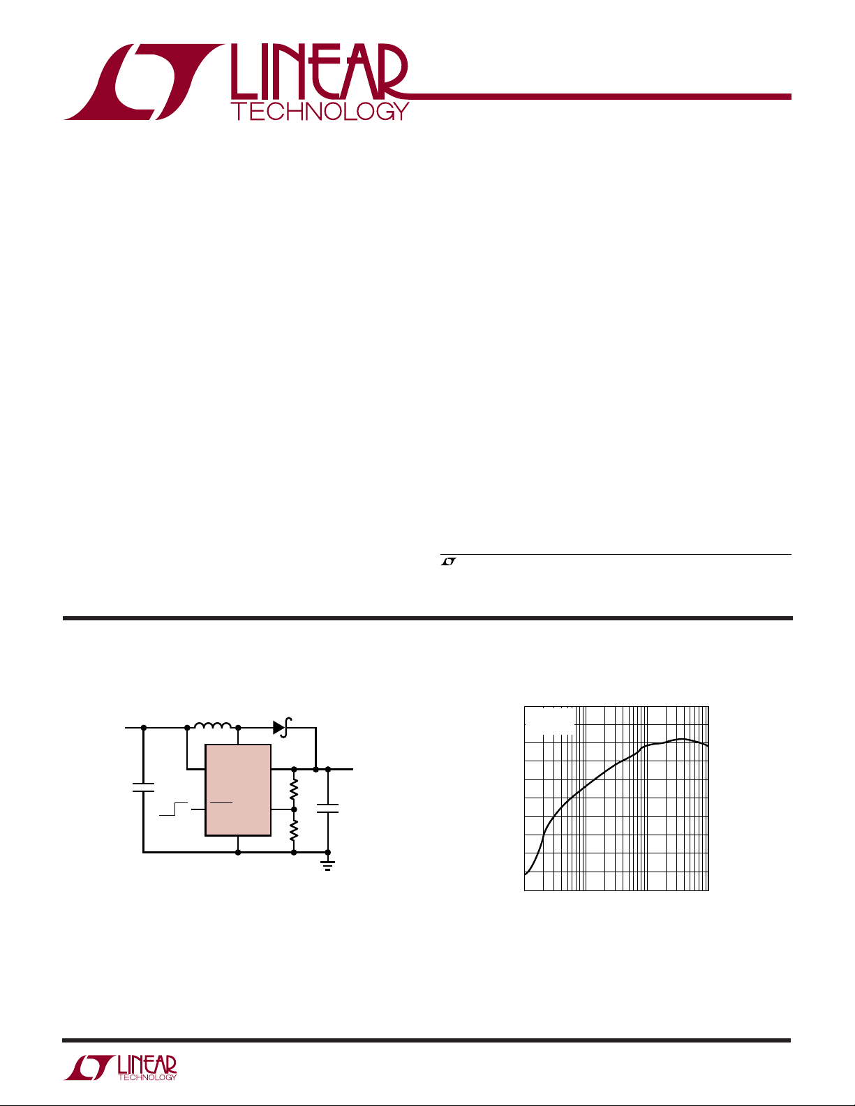
TYPICAL APPLICATIO
3.3V to 5V Boost Converter Efficiency
V
3.3V
IN
10µF
2.2µH
V
SHDN
SW
IN
LTC3426
GND
V
OUT
FBOFF ON
U
22µF
3426 TA01
V
OUT
5V
800mA
The LTC3426 is available in the 6-lead SOT-23 package.
, LT, LTC and LTM are registered trademarks of Linear Technology Corporation.
ThinSOT is a trademark of Linear Technology Corporation.
All other trademarks are the property of their respective owners.
Protected by U.S. Patents, including 6498466, 6611131
100
VIN = 3.3V
95
= 5V
V
OUT
90
85
80
75
70
EFFICIENCY (%)
65
60
55
50
1
10 100 1000
LOAD CURRENT (mA)
3426 TA01b
3426fa
1
LTC3426
W
O
A
(Note 1)
LUTEXI TIS
S
VIN Voltage ................................................. –0.3V to 6V
SW Voltage .................................................. – 0.3V to 6V
SHDN, FB Voltage ....................................... – 0.3V to 6V
V
........................................................... – 0.3V to 6V
OUT
Operating Temperature Range (Note 2) .. –40°C to 85°C
Storage Temperature Range ................. –65°C to 125°C
Lead Temperature (Soldering, 10 sec)................ 300°C
A
WUW
U
ARB
G
PACKAGE/ORDER I FOR ATIO
TOP VIEW
SW 1
GND 2
FB 3
S6 PACKAGE
6-LEAD PLASTIC TSOT-23
T
= 125°C, θJA = 165°C/W, θJC = 102°C/W
JMAX
ORDER PART NUMBER
UU
6 V
IN
5 V
OUT
4 SHDN
W
S6 PART NUMBER
LTC3426ES6 LTAJT
Order Options Tape and Reel: Add #TR
Lead Free: Add #PBF Lead Free Tape and Reel: Add #TRPBF
Lead Free Part Marking: http://www.linear.com/leadfree/
Consult LTC Marketing for parts specified with wider operating temperature ranges.
U
CO VERTER CHARACTERISTICS
temperature range, otherwise specifications are at T
PARAMETER CONDITIONS MIN TYP MAX UNITS
Input Voltage Range SHDN = V
Output Voltage Adjust Range 2.25 5 V
Feedback Voltage
Feedback Input Current VFB = 1.23V 0.1 µA
Quiescent Current (Shutdown) V
Quiescent Current SHDN = VIN, Not Switching 600 1000 µA
Switch Leakage VSW = 5V 0.2 10 µA
Switch On Resistance V
Current Limit
Maximum Duty Cycle VFB = 1.15V 80 85 %
Switching Frequency
SHDN Input High 1V
SHDN Input Low 0.4 V
SHDN Input Current SHDN = 5.5V 1 µA
V
SHDN
OUT
OUT
A
IN
= 0V, Not Including Switch Leakage 1 µA
= 3.3V 0.11 Ω
= 5V 0.10 Ω
The ● denotes the specifications which apply over the full operating
= 25°C. VIN = 1.8V, V
= 3.3V, unless otherwise specified.
OUT
1.6 V
●
1.173 1.22 1.247 V
●
●
2 2.3 A
0.85 1.2 1.5 MHz
Note 1: Stresses beyond those listed under Absolute Maximum Ratings
may cause permanent damage to the device. Exposure to any Absolute
Maximum Rating condition for extended periods may affect device
reliability and lifetime.
Note 2: The LTC3426 is guaranteed to meet performance specifications
from 0°C to 85°C. Specifications over the –40°C to 85°C operating
temperature are assured by design, characterization and correlation with
statistical process controls.
2
Note 3: This IC includes overtemperature protection that is intended to
protect the device during momentary overload conditions. Junction
temperature will exceed 125°C when overtemperature protection is active.
Continuous operation above the specified maximum operating junction
temperature may impair device reliability.
3426fa
UW
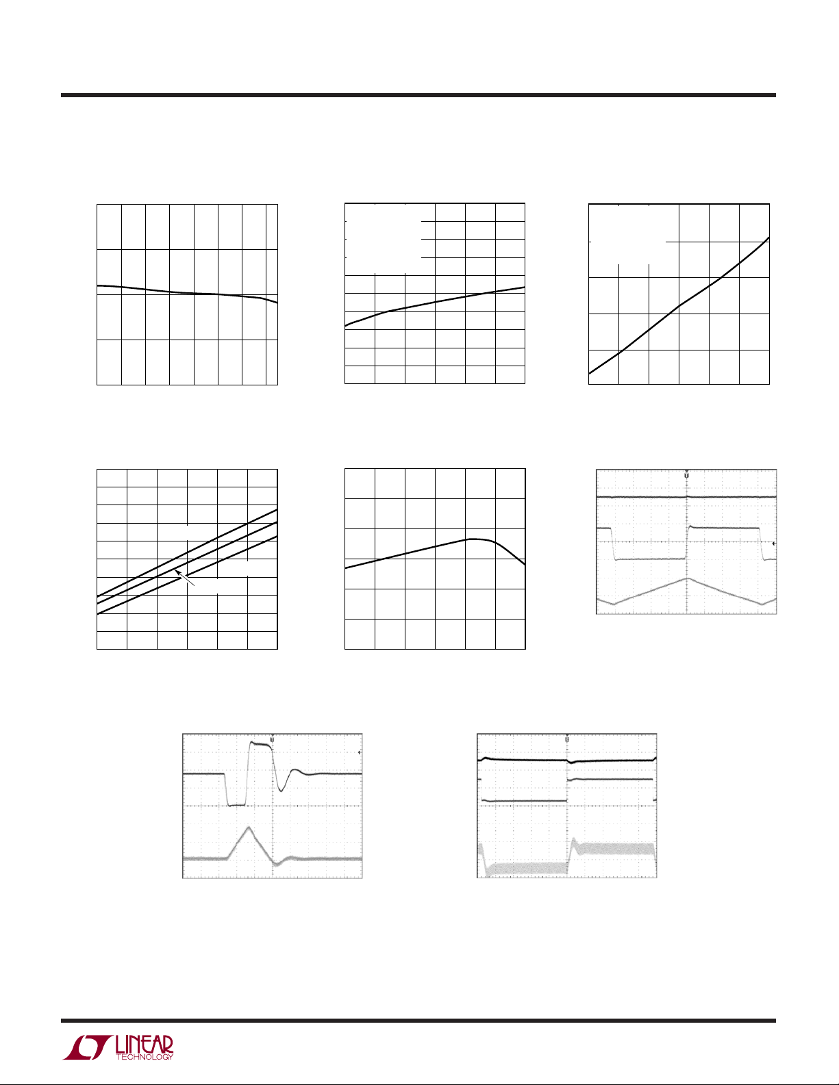
TYPICAL PERFOR A CE CHARACTERISTICS
Oscillator Frequency
vs Temperature
1.40
1.3
1.2
FREQUENCY (MHz)
1.1
1.0
–30 –10 10 30
–50
TEMPERATURE (°C)
50 70 90
3426 G01
Efficiency vs V
100
FIGURE 1 CIRCUIT
98
= 25°C
T
A
= 150mA
I
LOAD
96
= 5V
V
OUT
= 22µF
C
OUT
94
L = 2.2µH
92
90
88
EFFICIENCY (%)
86
84
82
80
1.8
2.2
2.6
IN
3 3.4
VIN (V)
3.8
LT1108 • TPC12
4.2
I
OUT(MAX)
1.3
FIGURE 1 CIRCUIT
T
V
1.1
C
L = 2.2µH
0.9
(A)
OUT(MAX)
0.7
I
0.5
0.3
1.8
= 25°C
A
OUT
OUT
vs V
= 5V
= 22µF
2.6 3 3.4
2.2
LTC3426
IN
3.8 4.2
VIN (V)
3426 G03
0.15
0.14
0.13
0.12
0.11
(Ω)
0.10
DS(ON)
0.09
R
0.08
0.07
0.06
0.05
R
–50
vs Temperature
DS(ON)
–25
TEMPERATURE (°C)
1V/DIV
50mA/DIV
V
= 2.5V
OUT
V
= 5V
OUT
V
= 3.3V
OUT
0
25 50
75
100
3426 G04
SW Pin Antiringing Operation
SW
I
L
V
= 1.8V
IN
OUT
= 3.3V
100ns/DIVV
FB Pin Voltage
1.25
1.24
1.23
1.22
FB VOLTAGE (V)
1.21
1.20
1.19
–50
–25
3426 G07
02550
TEMPERATURE (°C)
V
OUT
500mV/DIV
I
OUT
200mA/DIV
I
L
500mA/DIV
500mV/DIV
200mA/DIV
75 100
3426 G05
Transient Response
V
OUT
250mA
= 3.3V
V
OUT
= 22µF
C
OUT
L = 2.5µH
40µs/DIVVIN = 1.8V
Switching Waveforms
V
OUT
SW
2V/DIV
I
L
= 1.8V
IN
= 3.3V
V
OUT
= 22µF
C
OUT
L = 2.5µH
500mA
3426 G08
100ns/DIVV
3426 G06
3426fa
3
LTC3426
U
UU
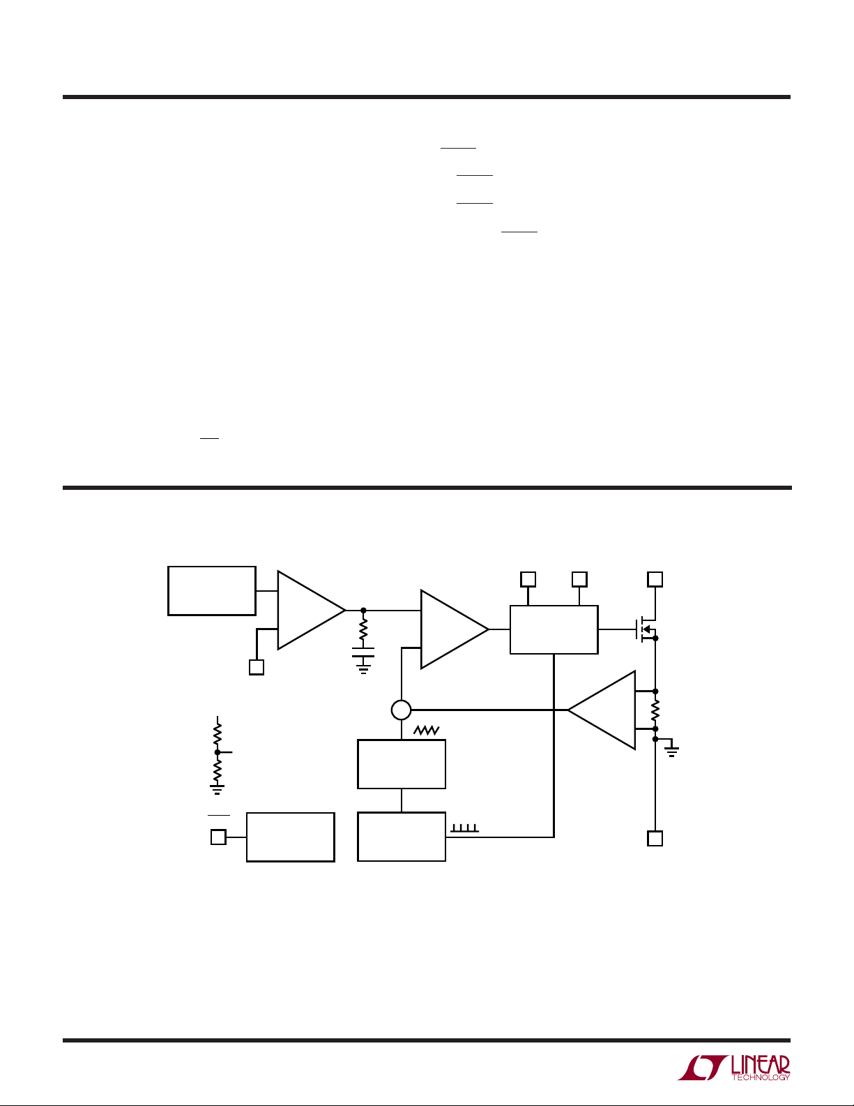
PI FU CTIO S
SW (Pin 1): Switch Pin. Connect inductor between SW and
V
. A Schottky diode is connected between SW and V
IN
OUT
.
Keep these PCB trace lengths as short and wide as
possible to reduce EMI and voltage overshoot. If the
inductor current falls to zero, an internal 100Ω antiringing
switch is connected from SW to V
to minimize EMI.
IN
GND (Pin 2): Signal and Power Ground. Provide a short
direct PCB path between GND and the (–) side of the output
capacitor(s).
FB (Pin 3): Feedback Input to the g
Error Amplifier.
m
Connect resistor divider tap to this pin. The output voltage
can be adjusted from 2.5V to 5V by:
R
1
V
=+
OUT
⎛
122 1
.•
⎜
⎝
⎞
⎟
⎠
R
2
W
BLOCK DIAGRA
SHDN (Pin 4): Logic Controlled Shutdown Input.
SHDN = High: Normal free running operation
SHDN = Low: Shutdown, quiescent current < 1µA
Typically, SHDN should be connected to VIN through a 1M
pull-up resistor.
(Pin 5): Output Voltage Sense Input. The NMOS
V
OUT
switch gate drive is derived from the greater of V
V
.
IN
(Pin 6): Input Supply. Must be locally bypassed.
V
IN
OUT
and
1.22V
REFERENCE
V
OUT
SHDN
4
3
FB
R1 (EXTERNAL)
FB
R2 (EXTERNAL)
SHUTDOWN AND
SOFT-START
V
OUT
+
A1
–
R
C
C
C
GENERATOR
1.2MHz
OSCILLATOR
COMPARATOR
–
A2
+
Σ
RAMP
Figure 1
5
PWM LOGIC
AND DRIVER
V
IN
6
SW
1
+
0.02Ω
–
2
3426 F01
GND
4
3426fa

OPERATIO
LTC3426
U
The LTC3426 is a monolithic 1.2MHz boost converter
housed in a 6-lead SOT-23 package. The device features
fixed frequency, current mode PWM control for excellent
line and load regulation. The low R
enables the device to maintain high efficiency over a wide
range of load current. Operation of the feedback loop
which sets the peak inductor current to keep the output in
regulation can be best understood by referring to the Block
Diagram in Figure 1. At the start of each clock cycle a latch
in the PWM logic is set and the NMOS switch is turned on.
The sum of a voltage proportional to the switch current
and a slope compensating voltage ramp is fed to the
positive input to the PWM comparator. When this voltage
exceeds either a voltage proportional to the 2A current
limit or the PWM control voltage, the latch in the PWM
logic is reset and NMOS switch is turned off. The PWM
NMOS switch
DS(ON)
WUUU
APPLICATIO S I FOR ATIO
Setting the Output Voltage
The output voltage, V
to ground. The divider tap is tied to the FB pin. V
V
OUT
is set by the formula:
V
=+
OUT
⎛
122 1
.•
⎜
⎝
, is set by a resistive divider from
OUT
R
1
⎞
⎟
⎠
R
2
OUT
control voltage at the output of the error amplifier is the
amplified and compensated difference between the feedback voltage on the FB pin and the internal reference
voltage of 1.22V. If the control voltage increases, more
current is delivered to the output. When the control voltage
exceeds the I
limited to a minimum of 2A. The current limit helps protect
the LTC3426 internal switch and external components
connected to it. If the control voltage decreases, less
current is delivered to the output. During load transients
control voltage may decrease to the point where no
switching occurs until the feedback voltage drops below
the reference. The LTC3426 has an integrated soft-start
feature which slowly ramps up the feedback control node
from 0V. The soft-start is initiated when SHDN is pulled
high.
to reduce the I
handle the peak inductor current without saturating.
Several inductor manufacturers are listed in Table 1.
Table 1. Inductor Manufacturers
Sumida www.sumida.com
reference voltage, the peak current is
LIMIT
2
R power losses, and must be able to
TDK www.tdk.com
Murata www.murata.com
Inductor Selection
The LTC3426 can utilize small surface mount inductors
due to its 1.2MHz switching frequency. A 1.5µH or 2.2µH
inductor will be the best choice for most LTC3426 applications. Larger values of inductance will allow greater
output current capability by reducing the inductor ripple
current. Increasing the inductance above 3.3µH will increase component size while providing little improvement in output current capability. The inductor current
ripple is typically set for 20% to 40% of the maximum
inductor current (IP). High frequency ferrite core inductor
materials reduce frequency dependent power losses compared to cheaper powdered iron types, improving efficiency. The inductor should have low DCR (DC resistance)
Output and Input Capacitor Selection
Low ESR (equivalent series resistance) capacitors should
be used to minimize the output voltage ripple. Multilayer
ceramic capacitors are an excellent choice as they have
extremely low ESR and are available in small footprints. A
15µF to 30µF output capacitor is sufficient for most
applications. X5R and X7R dielectric materials are preferred for their ability to maintain capacitance over wide
voltage and temperature ranges.
Low ESR input capacitors reduce input switching noise
and reduce the peak current drawn from the input supply.
It follows that ceramic capacitors are also a good choice
for input decoupling and should be located as close as
3426fa
5

LTC3426
WUUU
APPLICATIO S I FOR ATIO
possible to the device. A 10µF input capacitor is sufficient
for most applications. Table 2 shows a list of several
ceramic capacitor manufacturers. Consult the manufacturers for detailed information in their entire selection of
ceramic parts.
Table 2. Ceramic Capacitor Manufacturers
Taiyo Yuden www.t-yuden.com
Murata www.murata.com
TDK www.component.tdk.com
Diode Selection
A Schottky diode is recommended for use with the LTC3426.
Use of a low forward voltage diode such as the ON
Semiconductor MBRA210LT3 is recommended. A Schottky diode rated at 2A is recommended for use with the
LTC3426.
PCB Layout Guidelines
The high speed operation of the LTC3426 demands careful
attention to board layout. You will not get advertised
performance with careless layout. Figure 2 shows the
recommended component placement. A large ground pin
copper area will help to lower the chip temperature.
V
IN
6
SW
GND
FB
V
V
OUT
SHDN
IN
5
4
V
OUT
3426 F02
1
2
3
Figure 2. Recommended Component Placement
for Single Layer Board
6
3426fa

TYPICAL APPLICATIO S
L1
C1
10µF
2.2µH
V
SHDN
L1
1.5µH
V
SHDN
V
IN
3.3V
C1
10µF
C1: TAIYO YUDEN X5R JMK212BJ475ML
C2: TAIYO YUDEN X5R JMK316BJ226ML
D1: ON SEMICONDUCTOR MBRA210LT3
L1: COILCRAFT D03316P-222
V
IN
1.8V
C1: TDK C1608X5R0J106M
C2: TAIYO YUDEN JMK316BJ226ML
D1: ON SEMICONDUCTOR MBRM120LT3
L1: TDK RLF7030T-1R5N6R1
SW
IN
LTC3426
GND
IN
LTC3426
GND
V
SW
V
D1
OUT
FBOFF ON
D1
OUT
FBOFF ON
U
R1
95.3k
1%
R2
30.9k
1%
R1
64.9k
1%
R2
61.9k
1%
C2
22µF
3426 TA02a
C2
22µF
3426 TA03a
V
5V
800mA
V
OUT
2.5V
800mA
OUT
100
95
90
85
80
75
70
EFFICIENCY (%)
65
60
55
50
1
100
90
80
70
EFFICIENCY (%)
60
50
1
LTC3426
Efficiency
10 100 1000
LOAD CURRENT (mA)
3426 TA02b
Efficiency
10 100 1000
LOAD CURRENT (mA)
3426 TA03b
3426fa
7

LTC3426
TYPICAL APPLICATIO S
V
3V TO 4.2V
V
2.5V
L1
C1
10µF
C1
10µF
2.2µH
V
SHDN
L1
2.5µH
V
SHDN
SW
IN
LTC3426
GND
SW
IN
LTC3426
GND
IN
C1: TDK C1608X5R0J475M
C2: TAIYO YUDEN JMK316BJ226ML
D1: ON SEMICONDUCTOR MBR120VLSFT1
L1: SUMIDA CDRH4D28-2R2 2
IN
C1: TDK C1608X5R0J106
C2: TAIYO YUDEN JMK316BJ266
D1: ON SEMICONDUCTOR MBRM120LT3
L1: SUMIDA CDRH5D28-2R5 2
D1
V
OUT
FBOFF ON
D1
V
OUT
FBOFF ON
U
R1
95.3k
1%
R2
30.9k
1%
R1
75k
1%
R2
44.2k
1%
V
OUT
5V
750mA AT 3V
C2
22µF
3426 TA04a
V
OUT
3.3V
800mA
C2
22µF
3426 TA05a
100
95
90
85
80
75
70
EFFICIENCY (%)
65
60
55
50
1
100
90
80
70
EFFICIENCY (%)
60
50
1
Efficiency
VIN = 4.2V
VIN = 3V
10 100 1000
LOAD CURRENT (mA)
3426 TA04b
Efficiency
10 100 1000
LOAD CURRENT (mA)
3426 TA05b
8
3426fa

TYPICAL APPLICATIO S
L1
C1
10µF
C1
10µF
1.5µH
V
SHDN
L1
2.2µH
V
SHDN
IN
IN
V
IN
1.8V
C1: TDK C1608X5R0J106M
C2: TAIYO YUDEN JMK316BJ226ML
D1: ON SEMICONDUCTOR MBRM120LT3
L1: TDK RLF7030T-1R5N6R1
V
IN
1.8V
C1: TDK C1608X5R0J475M
C2: TAIYO YUDEN JMK316BJ226ML
D1: ON SEMICONDUCTOR MBR120VLSFT1
L1: SUMIDA CDRH4D28-2R2 2
SW
LTC3426
GND
SW
LTC3426
GND
D1
V
OUT
FBOFF ON
D1
V
OUT
FBOFF ON
U
R1
75k
1%
R2
44.2k
1%
R1
95.3k
1%
R2
30.9k
1%
C2
22µF
3426 TA06a
C2
22µF
3426 TA07a
V
OUT
3.3V
540mA
V
OUT
5V
400mA
100
90
80
70
EFFICIENCY (%)
60
50
1
90
80
70
60
EFFICIENCY (%)
50
40
1
LTC3426
Efficiency
10 100 1000
LOAD CURRENT (mA)
3426 TA06b
Efficiency
10 100 1000
LOAD CURRENT (mA)
3426 TA07b
3426fa
9

LTC3426
TYPICAL APPLICATIO S
L1
C1
10µF
2.5µH
V
SHDN
IN
V
IN
2.5V
C1: TDK C1608X5R0J106
C2: TAIYO YUDEN JMK316BJ266
D1: ON SEMICONDUCTOR MBRM120LT3
L1: SUMIDA CDRH5D28-2R5
SW
LTC3426
GND
D1
V
OUT
FBOFF ON
U
R1
95.3k
1%
R2
30.9k
1%
C2
22µF
3426 TA08a
V
OUT
5V
550mA
100
90
80
70
EFFICIENCY (%)
60
50
1
Efficiency
10 100 1000
LOAD CURRENT (mA)
3426 TA08b
10
3426fa

PACKAGE DESCRIPTIO
LTC3426
U
S6 Package
6-Lead Plastic TSOT-23
(Reference LTC DWG # 05-08-1636 Rev B)
0.62
MAX
3.85 MAX
2.62 REF
RECOMMENDED SOLDER PAD LAYOUT
PER IPC CALCULATOR
0.20 BSC
DATUM ‘A’
NOTE:
1. DIMENSIONS ARE IN MILLIMETERS
2. DRAWING NOT TO SCALE
3. DIMENSIONS ARE INCLUSIVE OF PLATING
4. DIMENSIONS ARE EXCLUSIVE OF MOLD FLASH AND METAL BURR
5. MOLD FLASH SHALL NOT EXCEED 0.254mm
6. JEDEC PACKAGE REFERENCE IS MO-193
0.95
REF
1.22 REF
1.4 MIN
0.30 – 0.50 REF
2.80 BSC
0.09 – 0.20
(NOTE 3)
1.50 – 1.75
(NOTE 4)
1.00 MAX
0.95 BSC
0.80 – 0.90
PIN ONE ID
2.90 BSC
(NOTE 4)
1.90 BSC
0.30 – 0.45
6 PLCS (NOTE 3)
0.01 – 0.10
S6 TSOT-23 0302 REV B
Information furnished by Linear Technology Corporation is believed to be accurate and reliable.
However, no responsibility is assumed for its use. Linear Technology Corporation makes no representation that the interconnection of its circuits as described herein will not infringe on existing patent rights.
3426fa
11

LTC3426
RELATED PARTS
PART NUMBER DESCRIPTION COMMENTS
LT1613 550mA (ISW), 1.4MHz, High Efficiency Step-Up 90% Efficiency, VIN: 0.9V to 10V, V
DC/DC Converter I
LT1946/LT1946A 1.5A (ISW), 1.2MHz/2.7MHz, High Efficiency Step-Up High Efficiency, VIN: 2.45V to 16V, V
DC/DC Converter I
LTC3400/LTC3400B 600mA (ISW), 1.2MHz, Synchronous Step-Up 92% Efficiency, VIN: 0.5V to 5V, V
DC/DC Converter I
LTC3401/LTC3402 1A/2A (ISW), 3MHz, Synchronous Step-Up DC/DC 97% Efficiency, VIN: 0.5V to 5V, V
Converter I
LTC3421 3A (ISW), 3MHz, Synchronous Step-Up DC/DC Converter 95% Efficiency, VIN: 0.5V to 4.5V, V
with Output Disconnect I
LTC3425 5A (ISW), 8MHz, 4-Phase Synchronous Step-Up DC/DC 95% Efficiency, VIN: 0.5V to 4.5V, V
Converter with Output Disconnect I
LTC3429 600mA (ISW), 550kHz, Synchronous Step-Up 90% Efficiency, VIN: 0.5V to 4.3V, V
DC/DC Converter with Soft-Start/Output Disconnect I
LTC3436 3A (ISW), 1MHz, High Efficiency Step-Up DC/DC Converter VIN: 3V to 25V, V
< 1µA, ThinSOT
SD
< 1µA, MS8
SD
< 1µA, ThinSOT
SD
< 1µA, MS10
SD
< 1µA, QFN24
SD
< 1µA, QFN32
SD
< 1µA, ThinSOT
SD
OUT(MAX)
OUT(MAX)
= 34V, IQ = 0.9mA, ISD < 6µA, TSSOP16E
OUT(MAX)
= 34V, IQ = 3mA,
OUT(MAX)
= 34V, IQ = 3.2mA,
OUT(MAX)
= 5V, IQ = 19µA/300µA,
= 5.5V, IQ = 38µA,
= 5.25V, IQ = 12µA,
OUT(MAX)
= 5.25V, IQ = 12µA,
OUT(MAX)
= 5V, IQ = 20µA,
OUT(MAX)
LTC3459 75mA (ISW), 10V Micropower Synchronous Boost VIN: 1.5V to 5.5V, V
Converter in ThinSOT
LTC3464 85mA (ISW), High Efficiency Step-Up DC/DC Converter VIN: 2.3V to 10V, V
with Schottky and PNP Disconnect
= 10V, IQ = 10µA, ISD < 1µA, ThinSOT
OUT(MAX)
= 34V, IQ = 25µA, ISD < 1µA, ThinSOT
OUT(MAX)
12
Linear Technology Corporation
1630 McCarthy Blvd., Milpitas, CA 95035-7417
(408) 432-1900 ● FAX: (408) 434-0507
●
www.linear.com
3426fa
LT 0307 REV A • PRINTED IN THE USA
© LINEAR TECHNOLOGY CORPORATION 2004
 Loading...