

Linear Technology LTC3412EFE Datasheet
FEATURES
LTC3412
2.5A, 4MHz, Monolithic
Synchronous Step-Down Regulator
U
DESCRIPTIO
■
High Efficiency: Up to 95%
■
2.5A Output Current
■
Low Quiescent Current: 62µA
■
Low R
■
Programmable Frequency: 300kHz to 4MHz
■
No Schottky Diode Required
■
±2% Output Voltage Accuracy
■
0.8V Reference Allows Low Output Voltage
■
Selectable Forced Continuous/Burst Mode Operation
Internal Switches: 85mΩ
DS(ON)
with Adjustable Burst Clamp
■
Synchronizable Switching Frequency
■
Low Dropout Operation: 100% Duty Cycle
■
Power Good Output Voltage Monitor
■
Overtemperature Protection
■
Available in 16-Lead Thermally Enhanced TSSOP
Package
U
APPLICATIO S
■
Portable Instruments
■
Battery-Powered Equipment
■
Notebook Computers
■
Distributed Power Systems
■
Cellular Telephones
■
Digital Cameras
The LTC®3412 is a high efficiency monolithic synchronous, step-down DC/DC converter utilizing a constant
frequency, current mode architecture. It operates from an
input voltage range of 2.625V to 5.5V and provides an
adjustable regulated output voltage from 0.8V to 5V while
delivering up to 2.5A of output current. The internal
synchronous power switch with 85mΩ on-resistance
increases efficiency and eliminates the need for an external Schottky diode. Switching frequency is set by an
external resistor or can be sychronized to an external
clock. 100% duty cycle provides low dropout operation
extending battery life in portable systems. OPTI-LOOP
®
compensation allows the transient response to be optimized over a wide range of loads and output capacitors.
The LTC3412 can be configured for either Burst Mode
®
operation or forced continuous operation. Forced continuous operation reduces noise and RF interference while
Burst Mode operation provides high efficiency by reducing gate charge losses at light loads. In Burst Mode
operation, external control of the burst clamp level allows
the output voltage ripple to be adjusted according to the
requirements of the application. To further maximize
battery life, the P-channel MOSFET is turned on continuously in dropout (100% duty cycle).
, LTC and LT are registered trademarks of Linear Technology Corporation.
Burst Mode and OPTI-LOOP are registered trademarks of Linear Technology Corporation.
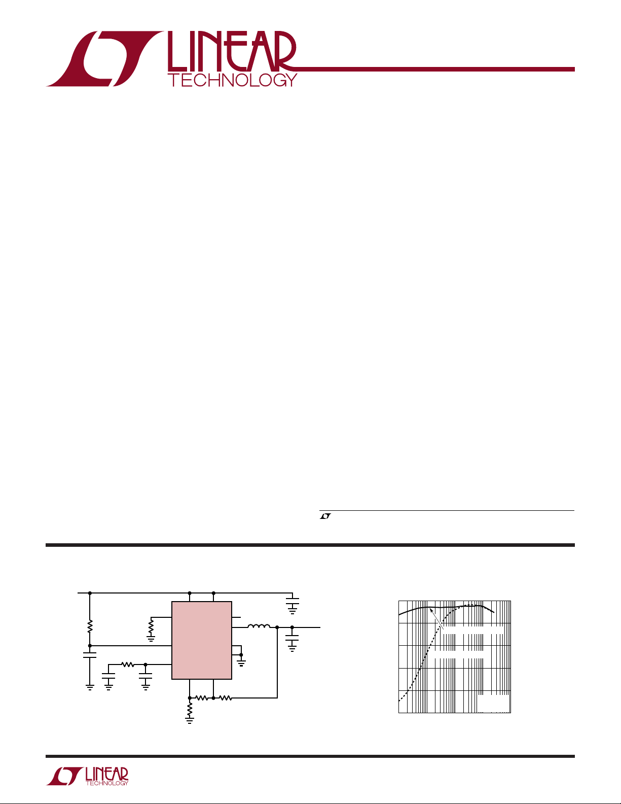
TYPICAL APPLICATIO
V
IN
2.7V TO 5.5V
SVINPV
R
T
4.7M
470pF
15k
1000pF
Figure 1. 2.5V, 2.5A Step-Down Regulator
309k
100pF
RUN/SS
I
TH
SYNC/MODE
LTC3412
110k
75k
U
PGOOD
V
FB
IN
PGND
SGND
SW
392k
1µH
3412 F01
22µF
100µF
V
2.5V
2.5A
OUT
Efficiency vs Load Current
100
80
60
40
EFFICIENCY (%)
20
0
0.001
Burst Mode OPERATION
FORCED CONTINUOUS
0.1 10.01
LOAD CURRENT (A)
VIN = 3.3V
= 2.5V
V
OUT
10
3412 G01
sn3412 3412fs
1
LTC3412
WW
W
ABSOLUTE AXI U RATI GS
U
UUW
PACKAGE/ORDER I FOR ATIO
(Note 1)
Input Supply Voltage ...................................– 0.3V to 6V
ITH, RUN, VFB Voltages ...............................–0.3V to V
SYNC/MODE Voltages ................................ –0.3V to V
IN
IN
SW Voltage ...................................–0.3V to (VIN + 0.3V)
Peak SW Sink and Source Current ......................... 6.5A
Operating Ambient Temperature
Range (Note 2) ....................................... – 40°C to 85°C
Junction Temperature (Note 5)............................. 125°C
Lead Temperature (Soldering, 10 sec).................. 300°C
ELECTRICAL CHARACTERISTICS
The ● denotes the specifications which apply over the full operating
TOP VIEW
1
SV
IN
2
PGOOD
3
I
TH
4
V
FB
5
R
T
SYNC/MODE
RUN/SS
EXPOSED PAD IS SGND (MUST BE SOLDERED TO PCB)
T
6
7
8
SGND
FE PACKAGE
16-LEAD PLASTIC TSSOP
= 125°C, θJA = 37.6°C/W, θJC = 10°C/W
JMAX
PV
16
IN
SW
15
SW
14
PGND
13
PGND
12
SW
11
SW
10
PV
9
IN
Consult LTC Marketing for parts specified with wider operating temperature ranges.
ORDER PART
NUMBER
LTC3412EFE
FE PART
MARKING
3412EFE
temperature range, otherwise specifications are at TA = 25°C. VIN = 3.3V unless otherwise specified.
SYMBOL PARAMETER CONDITIONS MIN TYP MAX UNITS
SV
IN
V
FB
I
FB
∆V
FB
V
LOADREG
∆V
PGOOD
R
PGOOD
I
Q
f
OSC
f
SYNC
R
PFET
R
NFET
I
LIMIT
V
UVLO
I
LSW
V
RUN
I
RUN
Signal Input Voltage Range 2.625 5.5 V
Regulated Feedback Voltage (Note 3) ● 0.784 0.800 0.816 V
Voltage Feedback Leakage Current 0.1 0.4 µA
Reference Voltage Line Regulation VIN = 2.7V to 5.5V (Note 3) ● 0.04 0.2 %/V
Output Voltage Load Regulation Measured in Servo Loop, V
Measured in Servo Loop, V
= 0.36V ● 0.02 0.2 %
ITH
= 0.84V ● –0.02 –0.2 %
ITH
Power Good Range ±7.5 ±9%
Power Good Pull-Down Resistance 120 200 Ω
Input DC Bias Current (Note 4)
Active Current V
= 0.78V, V
FB
Sleep VFB = 1V, V
Shutdown V
Switching Frequency R
RUN
OSC
= 0V, V
= 309kΩ 0.88 0.95 1.1 MHz
= 1V 250 330 µA
ITH
= 0V 62 80 µA
ITH
= 0V 0.02 1 µA
MODE
Switching Frequency Range (Note 6) 0.3 4 MHz
SYNC Capture Range (Note 6) 0.3 4 MHz
R
of P-Channel FET ISW = 1A 85 110 mΩ
DS(ON)
R
of N-Channel FET ISW = –1A 65 90 mΩ
DS(ON)
Peak Current Limit 4 5.4 A
Undervoltage Lockout Threshold 2.375 2.500 2.625 V
SW Leakage Current V
= 0V, VIN = 5.5V 0.1 1 µA
RUN
RUN Threshold 0.5 0.65 0.8 V
RUN/SS Leakage Current 1 µA
Note 1: Absolute Maximum Ratings are those values beyond which the life
of a device may be impaired.
Note 2: The LTC3412E is guaranteed to meet performance specifications
from 0°C to 70°C. Specifications over the –40°C to 85°C operating
temperature range are assured by design, characterization and correlation
with statistical process controls.
Note 3: The LTC3412 is tested in a feedback loop that adjusts V
to
FB
2
achieve a specified error amplifier output voltage (ITH).
Note 4: Dynamic supply current is higher due to the internal gate charge
being delivered at the switching frequency.
Note 5: T
dissipation as follows: LTC3412: T
is calculated from the ambient temperature TA and power
J
= TA + PD (37.6°C/W).
J
Note 6: 4MHz operation is guaranteed by design and not production tested.
sn3412 3412fs
UW
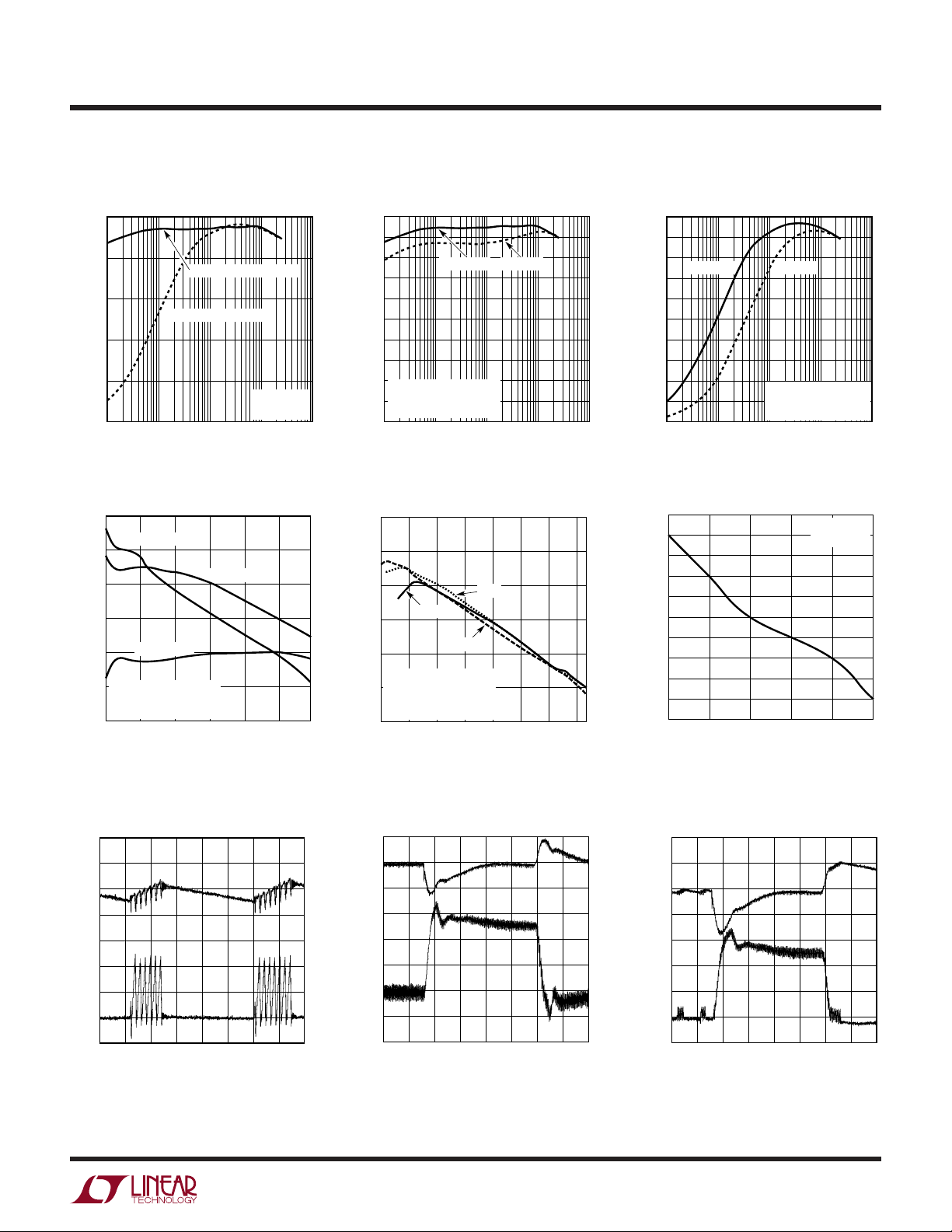
TYPICAL PERFOR A CE CHARACTERISTICS
Efficiency vs Load CurrentEfficiency vs Load Current Efficiency vs Load Current
100
80
60
40
EFFICIENCY (%)
20
0
0.001
Burst Mode OPERATION
FORCED CONTINUOUS
0.1 10.01
LOAD CURRENT (A)
VIN = 3.3V
= 2.5V
V
OUT
10
3412 G01
100
90
80
70
60
50
40
EFFICIENCY (%)
30
20
V
OUT
1MHz
10
Burst Mode OPERATION
0
0.001
VIN = 3.3V VIN = 5V
= 2.5V
0.1 10.01
LOAD CURRENT (A)
3412 G02
LTC3412
100
90
80
VIN = 3.3V VIN = 5V
70
60
50
40
EFFICIENCY (%)
30
20
10
10
0
0.001
V
= 2.5V
OUT
1MHz
FORCED CONTINUOUS
0.1 10.01
LOAD CURRENT (A)
10
3412 G03
98
LOAD = 100mA
96
94
92
EFFICIENCY (%)
90
88
86
OUT
V
LOAD = 2.5A
V
= 2.5V
OUT
1MHz
Burst Mode OPERATION
2.55 3.05 3.55 4.05 4.55 5.05
20mV/DIV
LOAD = 1A
INPUT VOLTAGE (V)
3412 G04
Efficiency vs FrequencyEfficiency vs Input Voltage
97
96
95
94
EFFICIENCY (%)
93
VIN = 3.3V
= 2.5V
V
92
OUT
LOAD = 1A
Burst Mode OPERATION
91
300
800 1300 1800 2300 2800 3300 3800
0.47µH
1µH
2.2µH
FREQUENCY (kHz)
Load Step Transient Forced
ContinuousBurst Mode Operation
OUT
V
100mV/DIV
3412 G05
Load Regulation
0.02
0.00
–0.02
–0.04
–0.06
OUT
/V
–0.08
OUT
–0.10
%∆V
–0.12
–0.14
–0.16
–0.18
0.5 1 1.5 2 2.5
0
LOAD CURRENT (A)
Load Step Transient Burst Mode
Operation
OUT
V
100mV/DIV
VIN = 3.3V
V
= 2.5V
OUT
3412 G06
L
I
200mA/DIV
VIN = 3.3V, V
LOAD = 50mA
OUT
4µs/DIV
= 2.5V
3412 G07
L
I
1A/DIV
20µs/DIV
VIN = 3.3V, V
LOAD STEP = NO LOAD TO 2.5A
OUT
= 2.5V
3412 G08
L
I
1A/DIV
VIN = 3.3V, V
LOAD STEP = 50mA TO 2.5A
OUT
= 2.5V
20µs/DIV
3412 G09
sn3412 3412fs
3
LTC3412
R
OSC
(kΩ)
50
150 250 350 450 550 650 750 850 950
FREQUENCY (kHz)
3412 G15
4500
4000
3500
3000
2500
2000
1500
1000
500
0
VIN = 3.3V
UW
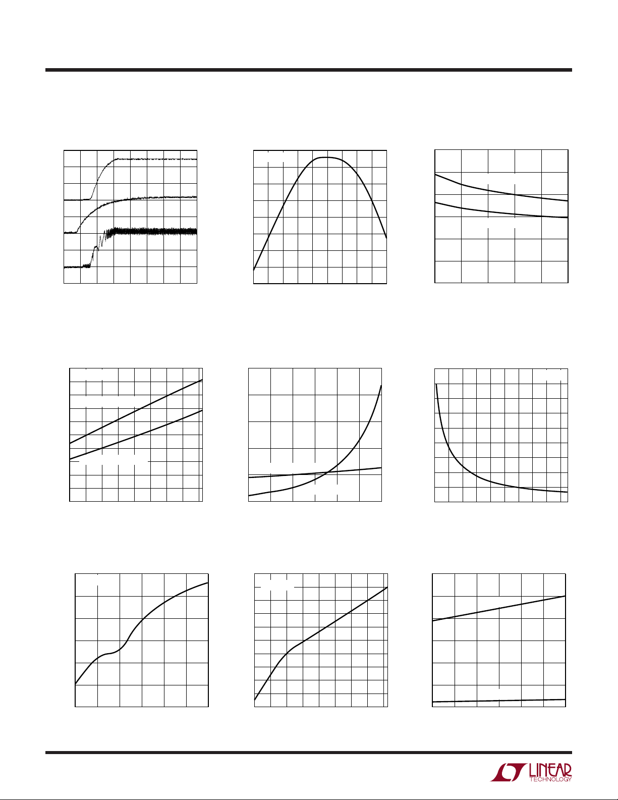
TYPICAL PERFOR A CE CHARACTERISTICS
Start-Up, Burst Mode Operation
OUT
V
1V/DIV
RUN
V
1V/DIV
L
I
1A/DIV
1ms/DIV
VIN = 3.3V, V
LOAD = 1Ω
OUT
= 2.5V
3412 G10
Reference Voltage
vs Temperature
0.7960
VIN = 3.3V
0.7955
0.7950
0.7945
0.7940
0.7935
0.7930
REFERENCE VOLTAGE (V)
0.7925
0.7920
–45 –25 –5 15 35 55 75 95 115 120
TEMPERATURE (°C)
3412 G11
Switch On-Resistance
vs Input Voltage
120
100
80
60
40
ON-RESISTANCE (mΩ)
20
0
2.5 3
Switch On-Resistance
vs Temperature Switch Leakage vs Input Voltage Frequency vs R
120
VIN = 3.3V
110
100
PFET ON-RESISTANCE
90
80
70
60
NFET ON-RESISTANCE
50
ON-RESISTANCE (mΩ)
40
30
20
–20 0 20 40 60 80 100 120
–40
TEMPERATURE (°C)
3412 G13
2.5
2.0
1.5
1.0
LEAKAGE CURRENT (nA)
SYNCHRONOUS SWITCH
0.5
0
2.5 3
3.5 4 4.5 5 5.5
INPUT VOLTAGE (V)
MAIN SWITCH
3412 G14
PFET ON-RESISTANCE
NFET ON-RESISTANCE
3.5 4 4.5 5
INPUT VOLTAGE (V)
3412 G12
OSC
4
Frequency vs Input Voltage
1050
R = 309k
1040
1030
1020
1010
FREQUENCY (kHz)
1000
990
3 3.5 4 4.5 5 5.5
2.5
INPUT VOLTAGE (V)
3412 G16
Switching Frequency
vs Temperature
1010
VIN = 3.3V
1008
1006
1004
1002
1000
998
FREQUENCY (kHz)
996
994
992
990
–20 0 20 40 60 80 100 120
–40
TEMPERATURE (°C)
3412 G17
DC Supply Current
vs Input Voltage
350
300
250
200
150
DC SUPPLY CURRENT (µA)
100
50
3 3.5 4 4.5 5 5.5
2.5
ACTIVE
SLEEP
INPUT VOLTAGE (V)
3412 G18
sn3412 3412fs
UW
INPUT VOLTAGE (V)
2.75
6.8
6.6
6.4
6.2
6.0
5.8
5.6
5.4
4.25 5.25
3412 G21
3.25 3.75
4.75
CURRENT LIMIT (A)
TYPICAL PERFOR A CE CHARACTERISTICS
Minimum Peak Inductor Current
DC Supply Current vs Temperature
350
VIN = 3.3V
300
250
200
150
100
SUPPLY CURRENT (µA)
50
0
–20 0 20 40 60 80 100 120
–40
ACTIVE
SLEEP
TEMPERATURE (°C)
3412 G19
vs Burst Clamp Voltage
4000
VIN = 3.3V
3500
3000
2500
2000
1500
1000
500
MINIMUM PEAK INDUCTOR CURRENT (mA)
0
0.2 0.3 0.4 0.5 0.6 0.7 0.8 0.9 1
0 0.1
BURST CLAMP VOLTAGE (V)
LTC3412
Current Limit vs Input Voltage
3412 G20
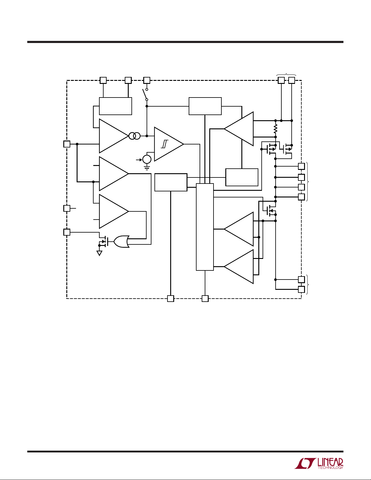
PI FU CTIO S
SVIN (Pin 1): Signal Input Supply. Decouple this pin to
SGND with a capacitor. Normally SVIN is equal to PVIN.
SVIN can be greater than PVIN but keep the voltage
difference between SVIN and PVIN less than 0.5V.
PGOOD (Pin 2): Power Good Output. Open-drain logic
output that is pulled to ground when the output voltage is
not within ±7.5% of regulation point.
ITH (Pin 3): Error Amplifier Compensation Point. The
current comparator threshold increases with this control
voltage. Nominal voltage range for this pin is from 0.2V to
1.4V with 0.2V corresponding to the zero-sense voltage
(zero current).
VFB (Pin 4): Feedback Pin. Receives the feedback voltage
from a resistive divider connected across the output.
RT (Pin 5): Oscillator Resistor Input. Connecting a resistor
to ground from this pin sets the switching frequency.
SYNC/MODE (Pin 6): Mode Select and External Clock
Synchronization Input. To select forced continuous, tie to
SVIN. Connecting this pin to a voltage between 0V and 1V
selects Burst Mode operation with the burst clamp set to
the pin voltage.
UUU
RUN/SS (Pin 7): Run Control and Soft-Start Input. Forcing
this pin below 0.5V shuts down the LTC3412. In shutdown
all functions are disabled drawing < 1µA of supply current.
A capacitor to ground from this pin sets the ramp time to
full output current.
SGND (Pin 8): Signal Ground. All small-signal components, compensation components and the exposed pad
on the bottom side of the IC should connect to this ground,
which in turn connects to PGND at one point.
PVIN (Pins 9, 16): Power Input Supply. Decouple this pin
to PGND with a capacitor.
SW (Pins 10, 11, 14, 15): Switch Node Connection to the
Inductor. This pin connects to the drains of the internal
main and synchronous power MOSFET switches.
PGND (Pins 12, 13): Power Ground. Connect this pin
close to the (–) terminal of CIN and C
OUT
.
sn3412 3412fs
5
LTC3412
UU
W
FU CTIO AL BLOCK DIAGRA
SGND
VOLTAGE
REFERENCE
0.8V
SV
IN
1
+
4
V
FB
0.74V
–
+
ERROR
AMPLIFIER
SYNC/MODE
–
+
RUNRUN/SS
7
0.86V
–
I
TH
3
+
–
–
+
OSCILLATOR
BCLAMP
BURST
COMPARATOR
SLOPE
COMPENSATION
RECOVERY
LOGIC
PMOS CURRENT
COMPARATOR
+
–
SLOPE
COMPENSATION
+
98
P-CH
N-CH
PV
IN
16
10
11
SW
14
15
PGOOD
2
NMOS
CURRENT
COMPARATOR
–
–
REVERSE
CURRENT
COMPARATOR
5
R
T
6
SYNC/MODE
+
3412 FBD
12
PGND
13
6
sn3412 3412fs
 Loading...