

Dual Output DC/DC Converter Solutions
for Xilinx FPGA Based Systems
Charlie Zhao
Design Solutions 41
February 2004
INTRODUCTION
Xilinx FPGAs require at least two power supplies: V
for core circuitry and V
for I/O interface. For the latest
CCO
CCINT
Xilinx FPGAs, including Virtex-II Pro, Virtex-II and Spartan-3, a third auxiliary supply, V
most cases, V
The core voltages, V
can share a power supply with V
CCAUX
, for most Xilinx FPGAs, range
CCINT
may be needed. In
CCAUX
CCO
.
from 1.2V to 2.5V. Some mature products have 3V, 3.3V
or 5V core voltages. Table 1 shows the core voltage
requirement for most of the FPGA device families. Typical
I/O voltages (V
voltage V
CCAUX
) vary from 1.2V to 3.3V. The auxiliary
CCO
is 2.5V for Virtex-II Pro and Spartan-3, and
is 3.3V for Virtex-II.
Each FPGA family has a specific quiescent supply current,
ranging from under 100mA to about 2A. For applications
with multiple FPGAs, the core supply current can be higher
than 10A.
With multiple voltage rails in today’s systems (FPGA, DDR
memory, data converter ICs, etc.), supply sequencing and
tracking are quite important for proper start-up and shutdown. Ramp time requirement should also be satisfied.
For example, the recommended ramp time (t
core voltage V
is less than 50ms during power-on.
CCINT
Some Xilinx FPGA families also have minimum V
CCPO
) for the
CCINT
ramp time requirements.
New dual output DC/DC regulators from Linear Technol-
ogy, the LTC®3407, LTC3736 and LTC3708, greatly simplify the design of an optimal power supply solution for
systems using Xilinx FPGAs.
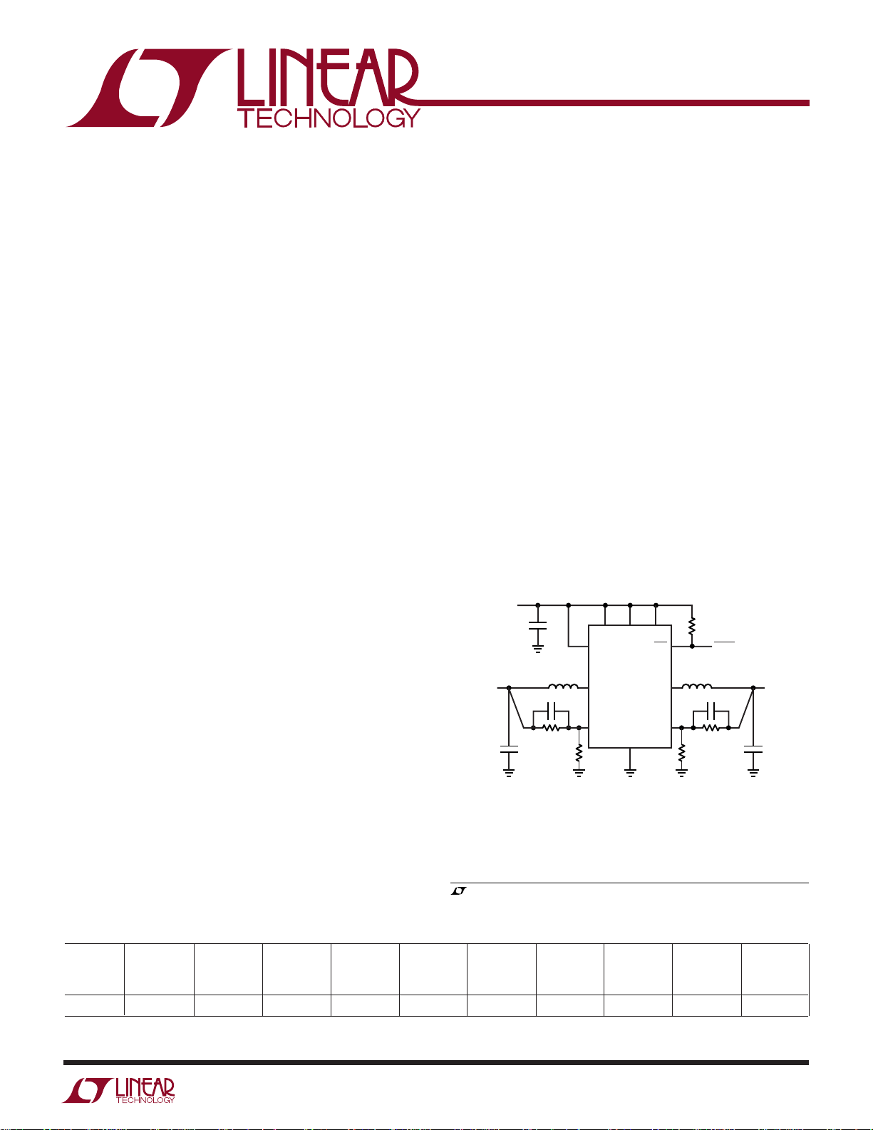
LTC3407: Dual Synchronous, 600mA, DC/DC
Regulator
The LTC3407 is a dual synchronous step-down DC/DC
converter with integrated power switches. It provides a
compact and high efficiency power solution for FPGAs
with supply currents up to 600mA. The switching regulator operates from a 2.5V to 5.5V input voltage range and
has an adjustable output range from 0.6V to 5V. Its internal
1A switches provide up to 96% efficiency, eliminating the
need for external MOSFETs and Schottky diodes. Figure 1
is an application example for 2.5V/600mA and 1.8V/
600mA supplies. Figure 2 shows the efficiency curves of
the circuit vs load current.
V
= 2.5V
IN
TO 5.5V
V
= 2.5V
OUT2
AT 600mA
C3
10µF
6.3V
C1, C2, C3: TAIYO YUDEN JMK316BJ106ML L1, L2: MURATA LQH32CN2R2M33
, LTC and LT are registered trademarks of Linear Technology Corporation.
Burst Mode is a registered trademark of Linear Technology Corporation.
R4
887k
C1
10µF
6.3V
L2
2.2µH
280k
R3
RUN2 V
MODE/SYNC
LTC3407
SW2
V
FB2
GND
RUN1
IN
POR
SW1
V
R5
100k
RESET
L1
2.2µH
C4 22pFC5 22pF
FB1
R1
443.5k
R2
887k
Figure 1. High Efficiency 2.5V/600mA
and 1.8V/600mA Regulators
V
OUT1
AT 600mA
C2
10µF
6.3V
= 1.8V
AN95 F01
Table 1. Core Voltage Requirement for Xilinx FPGA Families
Virtex-E
Extended
Virtex-II Pro Virtex-II Memory Virtex-E Virtex Spartan-3 Spartan-IIE Spartan-II Spartan-XL Spartan
V
CCINT
1.5V 1.5V 1.8V 1.8V 2.5V 1.2V 1.8V 2.5V 3.3V 5V
1
Design Solutions 41
100
95
90
85
80
75
EFFICIENCY (%)
70
VIN = 3.3V
65
Burst Mode OPERATION
NO LOAD ON OTHER CHANNEL
60
1
LOAD CURRENT (mA)
10 100 1000
2.5V
1.8V
AN95 F02
Figure 2. LTC3407 Efficiency Curve
The LTC3407 has a constant 1.5MHz switching frequency,
allowing the use of tiny inductors and capacitors. Selectable Burst Mode® operation provides high efficiency at
light loads. The IC has short-circuit protection and a
power-on reset (power good) output. It is available in
small thermally enhanced 10-lead MSOP and 3 × 3 DFN
packages.
load current requirements for most FPGA applications.
The LTC3736 receives input from 2.7V to 9.8V and produces output voltages ranging from 0.6V to 9.5V. Figure␣ 3
shows that up to 95% efficiency is achieved. An application example is shown in Figure 4.
In contrast to single-phase operation, the two channels of
a 2-phase switching converter are operated 180 degrees
out of phase. This technique interleaves the current pulses
coming from the topside MOSFET switches, greatly
reducing the total RMS input ripple current. This in
turn allows the use of smaller and lower cost input
capacitors, reduces the EMI attenuation requirement and
improves operating efficiency.
100
90
80
70
EFFICIENCY (%)
60
VO = 2.5V
VO = 1.8V
LTC3736: 2-Phase, Dual Synchronous, DC/DC
Controller for 5A Loads
The LTC3736 is a 2-phase dual synchronous step down
DC/DC controller. Power supplies using the LTC3736 can
provide 5A at both outputs with a 5V input, meeting the
C3
1µF
20
21
17
22
19
18
14
6
23
24
1
10V
LTC3736
PGND1
SENSE1
TG1
SW1
BG1
SYNC/FCB
RUN/SS
TRACK
I
PRG1
V
FB1
I
TH1
V
+
V
(5A AT 5V
OUT1
2.5V
IN
)
+
Si7540DP
Q1A
Si7540DP
C6
150µF
4V
Q1B
1.5µH
IHLP2525CZ-01
R3
118k
1%
R4
187k
1%
L1
C11
220pF
R7
59k
1%
R6
59k
1%
15k
R8
R1
10Ω
525
IN
PGND
12
PGND2
11
SENSE2+
15
TG2
10
SW2
13
BG2
16
PGND
9
PGOOD
3
PLLLPF
2
I
PRG2
7
V
FB2
8
I
TH2
4
50
40
10
1 100 1000 10000
LOAD CURRENT (mA)
Figure 3. Efficiency vs Load Current
for the LTC3736 Converter
C1
22µF
R2
10V
1M
R9
15k
C14
220pF
AN95 F04
IHLP2525CZ-01
R10
59k
1%
L2
1.5µH
R5
118k
1%
Q2B
Si7540DP
Q2A
Si7540DP
150µF
+
C9
4V
VIN = 3.3V
V
IN
2.7V TO 9.8V
V
OUT2
1.8V
(5A AT 5V
AN95 F03
)
IN
2
Figure 4. High Efficiency 2.5V/5A and 1.8V/5A Dual Output Converter with Output Tracking

Design Solutions 41
Figure 5 compares the input waveforms for a representative single-phase dual switching converter to the 2-phase
dual switching converter. Figure 6 shows how the RMS
input current varies for single phase and 2-phase dual
controllers with 2.5V and 1.8V outputs over a wide input
voltage range. For most applications, 2-phase operation
will reduce the input capacitor RMS current requirement
to that of just one channel operating at maximum current
and 50% duty cycle.
The LTC3736 has a default switching frequency at 550kHz,
but can be externally synchronized from 300kHz to 750kHz.
The LTC3736 provides output tracking for controlled
ramp-up of two supply rails, programmable current limit,
output overvoltage protection, power good output and
selectable Burst Mode operation for high efficiency light
load operations. The IC is available in the tiny (4mm ×
4mm) thermally enhanced QFN package or the 24-lead
SSOP package.
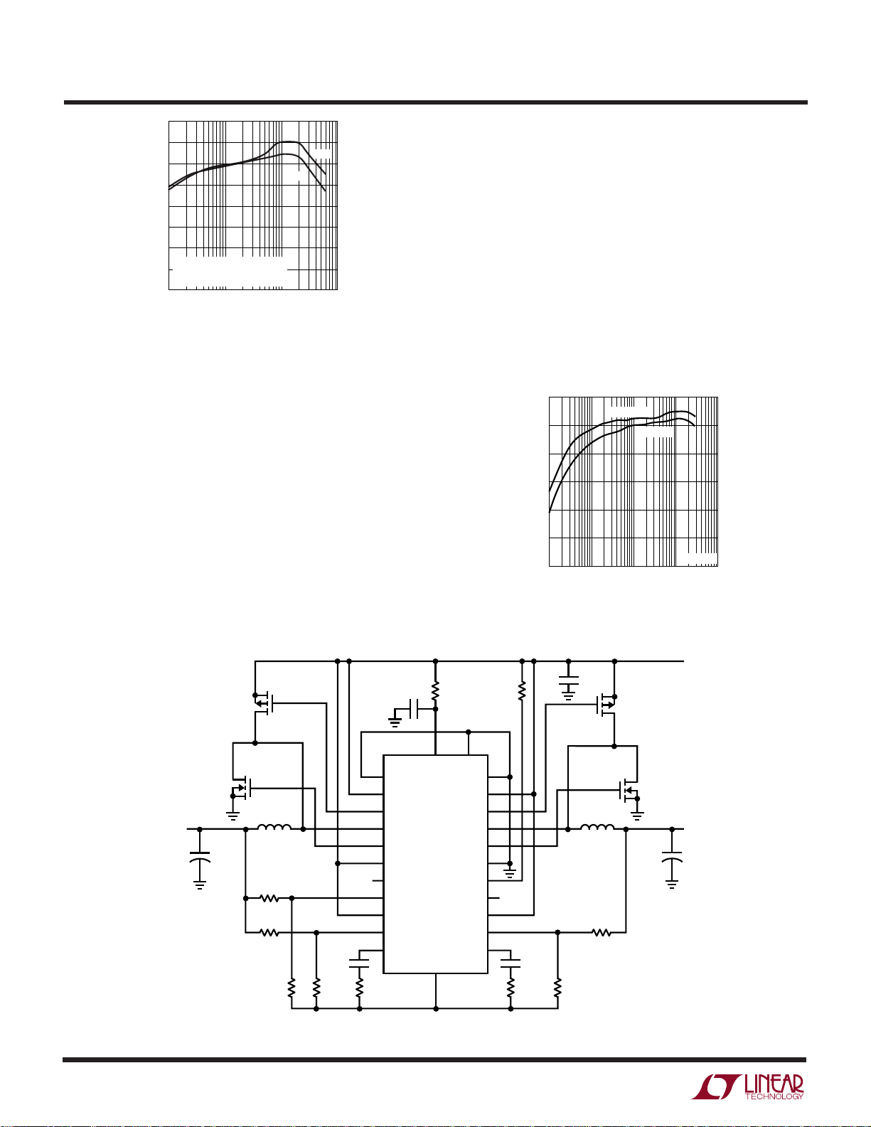
LTC3708: 2-phase, Dual Synchronous, DC/DC
Controller for 15A Loads
The core supply voltages of the latest Xilinx FPGAs have
decreased towards 1V. The Virtex-II pro family requires
1.5V V
V
CCINT
and the Spartan-3 family needs only 1.2V
CCINT
. In the meantime, these FPGAs demand more
current from the power supplies. Some systems use more
than ten FPGAs per board so the resulting total supply
current can easily exceed 10A. The LTC3708-based dual
output supply is an ideal choice for such applications.
Single Phase
Dual Controller
SW1 (V)
SW2 (V)
2-Phase
Dual Controller
The LTC3708 is a 2-phase dual synchronous step-down
DC/DC controller with a wide input voltage range: from
3.3V up to 36V. Its output voltage can be programmed
down to 0.6V. Figure 7 shows the schematic of a dual
output 2.5V/15A and 1.8V/15A converter. As shown in
Figure 8, up to 95% efficiency can be achieved.
The LTC3708 has output voltage up/down tracking capability. The IC allows both coincident or ratiometric tracking, as shown in Figures 9 and 10. The ramp rate can be
selected by a soft-start capacitor from RUN/SS pin to
ground. Multiple LTC3708s can easily be daisy-chained in
applications requiring more than two voltages to be tracked.
The 2-phase operation of the LTC3708 reduces power loss
and noise, and lowers the input-filtering requirement. The
constant on time, valley current mode control in the
LTC3708 allows fast transient response and thus minimizes the number of output capacitors. An internal phaselocked loop allows the IC to be synchronized to an external
clock for applications with more than two output rails. The
LTC3708 also features programmable current limit, output overvoltage protection and power good output. The IC
is available in the 5mm × 5mm QFN package.
Conclusion
An optimal power solution for multirail supply systems
incorporating the latest Xilinx FPGAs should provide multiple outputs with supply tracking/sequencing. As board
real estate becomes more expensive, the power supply
must be more efficient and smaller while supplying higher
current in high-end applications. Linear Technology’s
latest dual output power management ICs: LTC3407,
LTC3736 and LTC3708, successfully address these challenges. For data sheets and additional information on
other power solutions for Xilinx FPGAs, visit Linear
Technology’s web site at www.linear.com.
I
L1
I
L2
I
IN
AN95 F05
Figure 5. Example Waveforms for a Single-Phase
Dual Converter vs the 2-Phase LTC3736
Information furnished by Linear Technology Corporation is believed to be accurate and reliable.
However, no responsibility is assumed for its use. Linear Technology Corporation makes no representation that the interconnection of its circuits as described herein will not infringe on existing patent rights.
2.0
1.8
1.6
1.4
1.2
1.0
0.8
0.6
0.4
INPUT CAPACITOR RMS CURRENT
V
OUT1
0.2
V
OUT2
0
2
SINGLE PHASE
DUAL CONTROLLER
DUAL CONTROLLER
= 2.5V/2A
= 1.8V/2A
35
6
4
INPUT VOLTAGE (V)
2- PHASE
7
9
8
10
AN95 F06
Figure 6. RMS Input Current Comparision
3

Design Solutions 41
V
IN
3.3V TO 28V
C
IN
10µF
35V
×4
CMDSH-3
5V
+
4.7µF
1µF
10Ω
CMDSH-3
M1, M2: RENESAS HAT2168
M3, M4: RENESAS HAT2165
COUT1: SANYO POSCAP 4TPD330M
COUT2: SANYO POSCAP 2R5TPD470M
L1, L2: PANASONIC ETQP3H
V
OUT1
2.5V
15A
M1
L1
1.4µH
19.1k
6.04k
B340A
D1
12.1k
C
OUT1
+
330µF
4V
×2
6.04k
0.22µF 0.22µF
M3
1.5M 1.07M
V
IN
33k 33k10k 10k
0.01µF
180pF
17 21 30
VCCDRV
27
TG1
28
BOOST1
26
25
22
24
23
3
6
29
2
10
1
0.1µF
LTC3708
SW1
+
SENSE1
BG1
–
SENSE1
PGND1
V
FB1
TRACK2
I
ON1
I
TH1
INTLPF
RUN/SS
SGND VRNG1 VRNG2
53211
CC
PWRGD
TG2
BOOST2
SW2
SENSE2+
BG2
SENSE2–
PGND2
V
FB2
FCB
I
ON2
I
TH2
EXTLPF
TRACK1
25k
14
13
15
16
20
18
19
7
31
12
8
9
4
100k
M2
M4
f
IN
V
IN
0.01µF
5V
Figure 7. High Efficiency 2.5V/15A and 1.8V/15A Dual Output Converter with Output Tracking
100
95
D2
B340A
180pF
L2
1.2µH
AN95 F07
12.1k
6.04k
V
OUT2
1.8V
15A
C
OUT2
+
470µF
2.5V
×2
Figure 8. Efficiency vs Load Current for the LTC3708 Converter
500mV/DIV
2ms/DIV
Figure 9. Up/Down Coincident Tracking
90
85
EFFICIENCY (%)
80
75
70
0.01
AN95 F09
20VIN TO 2.5V
5V
IN
20V
5V
IN
0.1 1 10 15
LOAD CURRENT (A)
TO 2.5V
TO 1.8V
IN
TO 1.8V
OUT
OUT
OUT
OUT
AN95 F08
500mV/DIV
2ms/DIV
AN95 F10
Figure 10. Up/Down Ratiometric Tracking
Linear Technology Corporation
1630 McCarthy Blvd., Milpitas, CA 95035-7417
4
(408) 432-1900 ● FAX: (408) 434-0507 ● www.linear.com
dsol41 LT/TP 0204 1K • PRINTED IN USA
LINEAR TECHNOLOGY CORPORATION 2004
 Loading...