

Linear Technology LTC3400BES6, LTC3400ES6 Datasheet
FEATURES
■
Up to 92% Efficiency
■
Generates 3.3V at 100mA from a Single AA Cell
■
Low Start-Up Voltage: 0.85V
■
1.2MHz Fixed Frequency Switching
■
Internal Synchronous Rectifier
■
2.5V to 5V Output Range
■
Automatic Burst Mode® Operation (LTC3400)
■
Continuous Switching at Light Loads (LTC3400B)
■
Logic Controlled Shutdown (<1µA)
■
Antiringing Control Minimizes EMI
■
Tiny External Components
■
Low Profile (1mm) ThinSOTTM Package
U
APPLICATIO S
■
Pagers
■
MP3 Players
■
Digital Cameras
■
LCD Bias Supplies
■
Handheld Instruments
■
Wireless Handsets
■
GPS Receivers
LTC3400/LTC3400B
600mA, 1.2MHz Micropower
Synchronous Boost Converter
in ThinSOT
U
DESCRIPTIO
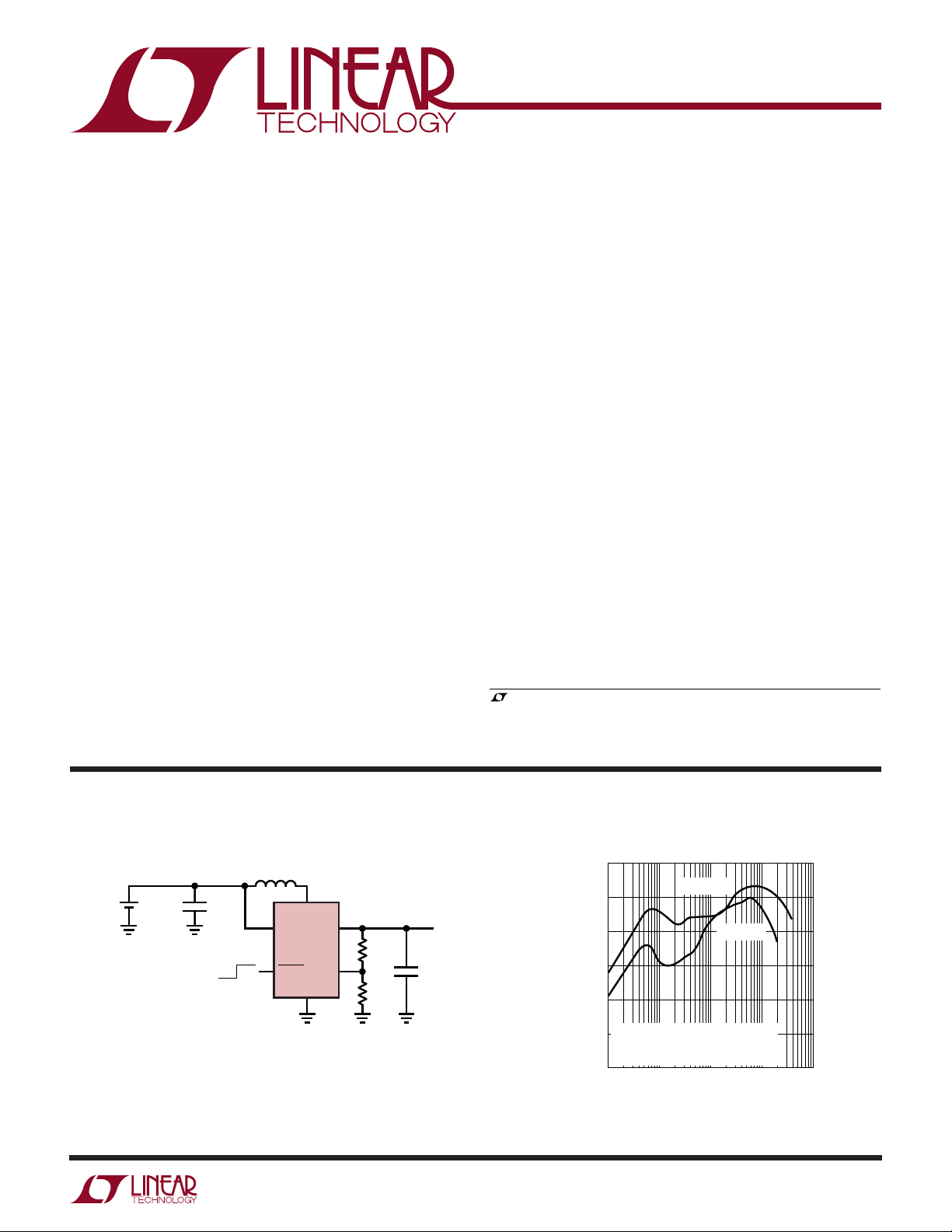
The LTC®3400/LTC3400B are synchronous, fixed frequency, step-up DC/DC converters delivering high efficiency in a 6-lead ThinSOT package. Capable of supplying
3.3V at 100mA from a single AA cell input, the devices
contain an internal NMOS switch and PMOS synchronous
rectifier.
A switching frequency of 1.2MHz minimizes solution
footprint by allowing the use of tiny, low profile inductors
and ceramic capacitors. The current mode PWM design is
internally compensated, reducing external parts count.
The LTC3400 features automatic shifting to power saving
Burst Mode operation at light loads, while the LTC3400B
features continuous switching at light loads. Antiringing
control circuitry reduces EMI concerns by damping the
inductor in discontinuous mode, and the devices feature
low shutdown current of under 1µA.
Both devices are available in the low profile (1mm) ThinSOT
package.
, LTC, LT and Burst Mode are registered trademarks of Linear Technology Corporation.
ThinSOT is a trademark of Linear Technology Corporation.
TYPICAL APPLICATIO
L1
4.7µH
+
SINGLE
AA CELL
C1, C2: TAIYO-YUDEN X5R EMK316BJ475ML
L1: COILCRAFT DO160C-472
Figure 1. Single Cell to 3.3V Synchronous Boost Converter
C1
4.7µF
OFF
ON
6
4
V
IN
LTC3400
SHDN
SW
GND
U
Efficiency
100
1
V
C2
4.7µF
3400 F01
OUT
3.3V
100mA
5
V
OUT
2
R1
1.02M
1%
3
FB
R2
604k
1%
90
80
70
EFFICIENCY (%)
60
FIGURE 1 CIRCUIT
50
WITH OPTIONAL SCHOTTKY DIODE
(SEE APPLICATIONS INFORMATION)
40
0.1 10 100 1000
VIN = 2.4V
VIN = 1.5V
1
LOAD CURRENT (mA)
3400 F01a
3400f
1
LTC3400/LTC3400B
PACKAGE/ORDER I FOR ATIO
UU
W
WWWU
ABSOLUTE AXI U RATI GS
(Note 1)
VIN Voltage ................................................. –0.3V to 6V
SW Voltage ................................................. –0.3V to 6V
SHDN, FB Voltage ....................................... –0.3V to 6V
V
........................................................... –0.3V to 6V
OUT
Operating Temperature Range (Note 2) .. – 30°C to 85°C
Storage Temperature Range ................... – 65°C to 125°
Lead Temperature (Soldering, 10 sec)..................300°C
ORDER PART
TOP VIEW
SW 1
GND 2
FB 3
S6 PACKAGE
6-LEAD PLASTIC SOT-23
T
= 125°C, θJA = 256°C/W
JMAX
6 V
IN
5 V
OUT
4 SHDN
NUMBER
LTC3400ES6
LTC3400BES6
S6 PART MARKING
LTWK
LTUN
Consult LTC Marketing for parts specified with wider operating temperature ranges.
ELECTRICAL CHARACTERISTICS
temperature range, otherwise specifications are at TA = 25°C. VIN = 1.2V, V
PARAMETER CONDITIONS MIN TYP MAX UNITS
Minimum Start-Up Voltage I
Minimum Operating Voltage SHDN = VIN (Note 4) 0.5 0.65 V
Output Voltage Adjust Range 2.5 5 V
Feedback Voltage ● 1.192 1.23 1.268 V
Feedback Input Current VFB = 1.25V (Note 3) 1 nA
Quiescent Current (Burst Mode Operation) VFB = 1.4V (Note 5), LTC3400 Only 19 30 µA
Quiescent Current (Shutdown) V
Quiescent Current (Active) Measured On V
NMOS Switch Leakage VSW = 5V 0.1 5 µA
PMOS Switch Leakage VSW = 0V 0.1 5 µA
NMOS Switch On Resistance V
PMOS Switch On Resistance V
NMOS Current Limit 600 850 mA
Burst Mode Operation Current Threshold LTC3400 Only (Note 3) 3 mA
Current Limit Delay to Output (Note 3) 40 ns
Max Duty Cycle VFB = 1.15V ● 80 87 %
Switching Frequency 0.95 1.2 1.5 MHz
SHDN Input High 1V
SHDN Input Low 0.35 V
SHDN Input Current V
LOAD
SHDN
OUT
V
OUT
OUT
V
OUT
SHDN
The ● denotes the specifications which apply over the full operating
= 3.3V, unless otherwise specified.
OUT
= 1mA 0.85 1 V
= 0V, Not Including Switch Leakage 0.01 1 µA
OUT
= 3.3V 0.35 Ω
= 5V 0.20 Ω
= 3.3V 0.45 Ω
= 5V 0.30 Ω
● 0.85 1.2 1.5 MHz
= 5.5V 0.01 1 µA
300 500 µA
Note 1: Absolute Maximum Ratings are those values beyond which the life
of a device may be impaired.
Note 2: The LTC3400E/LTC3400BE are guaranteed to meet performance
specifications from 0°C to 70°C. Specifications over the –30°C to 85°C
operating temperature range are assured by design, characterization and
correlation with statistical process controls.
2
Note 3: Specification is guaranteed by design and not 100% tested in
production.
Note 4: Minimum V
battery’s ability to provide the necessary power as it enters a deeply
discharged state.
Note 5: Burst Mode operation I
by V
to get the equivalent input (battery) current.
OUT/VIN
operation after start-up is only limited by the
IN
is measured at V
Q
. Multiply this value
OUT
3400f
UW
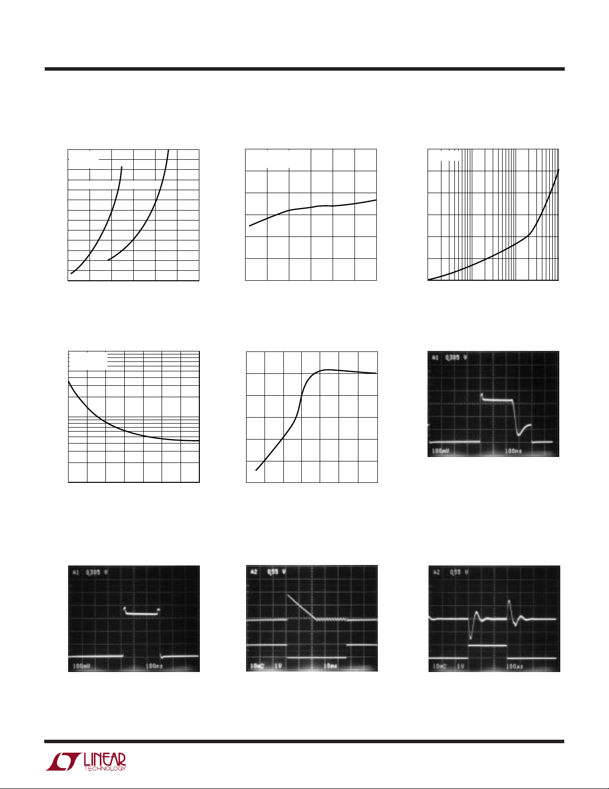
TYPICAL PERFOR A CE CHARACTERISTICS
LTC3400/LTC3400B
Output Load Burst Mode Threshold
vs V
IN
L = 4.7µH
= 25°C
T
A
20
V
= 3.3V V
OUT
10
OUTPUT CURRENT (mA)
0
0.9
1.5 2.1 2.7 3.3
OUT
VIN (V)
= 5V
No Load Battery Current vs V
1000
V
= 3.3V
OUT
= 25°C
T
A
100
3.9 4.5
3400 G01
BATT
V
vs Temperature
OUT
3.36
FIGURE 1 CIRCUIT
I
= 10mA
O
3.34
3.32
(V)
3.30
OUT
V
3.28
3.26
3.24
–60
03060
–30
TEMPERATURE (°C)
Normalized Oscillator Frequency
vs Temperature
1.01
1.00
0.99
0.98
90 120
3400 G02
Minimum Start-Up Voltage
vs Load Current
1.4
TA = 25°C
1.3
1.2
1.1
1.0
START-UP VOLTAGE (V)
0.9
0.8
0.1
1 10 100
I
(mA) CURRENT SOURCE LOAD
OUT
SW Pin Antiringing Operation
V
SW
1V/DIV
3400 G03
BATTERY CURRENT (µA)
10
0.9
1.2
1.8
BATTERY VOLTAGE (V)
SW Pin Fixed Frequency,
Continuous Inductor Current
Operation
V
SW
1V/DIV
0V
= 1.3V 100ns/DIV 3400 G07
V
IN
V
= 3.3V
OUT
= 50mA
I
OUT
L = 6.8µH
C
= 4.7µF
OUT
2.1 2.4 2.7
3400 G04
3.01.5
0.97
NORMALIZED FREQUENCY
0.96
0.95
–50
–30 –10
Fixed Frequency and Burst Mode
Operation V
V
OUT(AC)
100mV/DIV
60mA
I
OUT
10µA
V
= 1.3V 10ms/DIV 3400 G08
IN
V
= 3.3V
OUT
= 60mA TO 10µA
I
OUT
L = 6.8µH
C
= 4.7µF
OUT
30 70 90
10 50
TEMPERATURE (°C)
3400 G05
0V
V
OUT(AC)
100mV/DIV
100mA
I
OUT
40mA
= 1.3V 100ns/DIV 3400 G06
V
IN
V
= 3.3V
OUT
I
= 10mA
OUT
L = 6.8µH
= 4.7µF
C
OUT
Transient Response
OUT
V
= 1.3V 100µs/DIV 3400 G09
IN
V
= 3.3V
OUT
= 40mA TO 100mA
I
OUT
L = 6.8µH
C
= 4.7µF
OUT
3400f
3
LTC3400/LTC3400B
U
UU
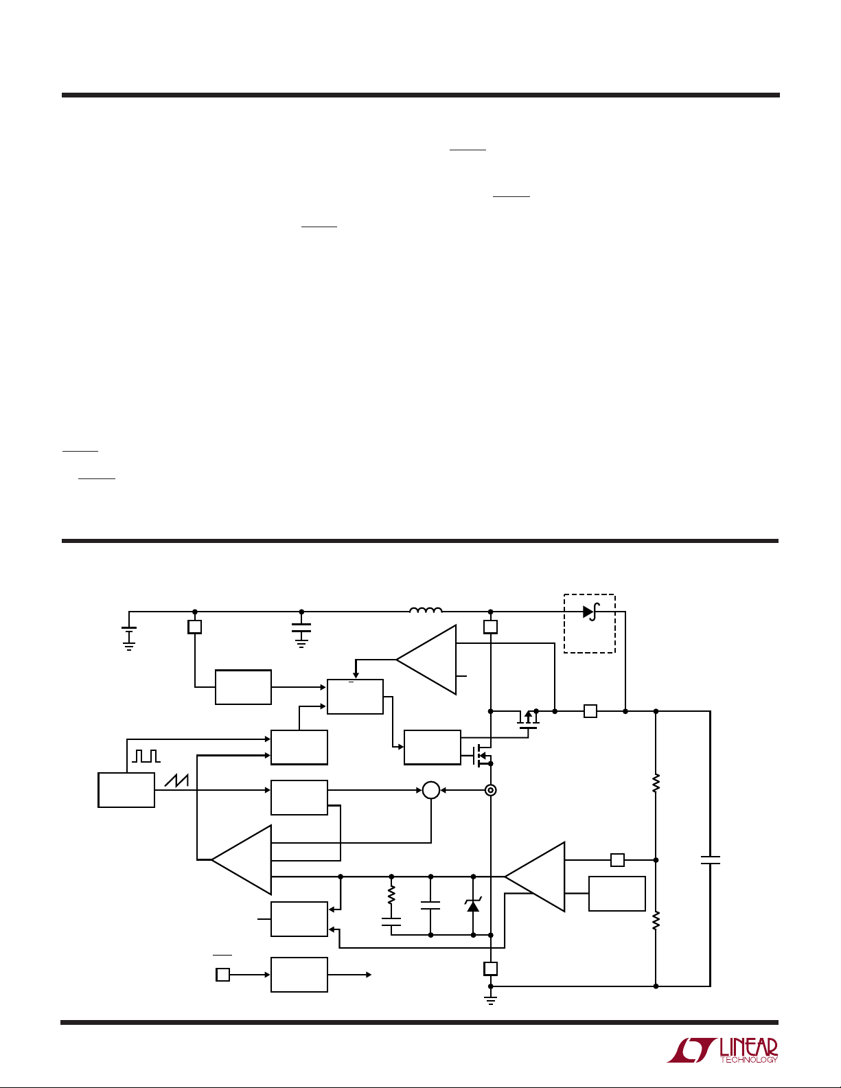
PI FU CTIO S
SW (Pin 1): Switch Pin. Connect inductor between SW
and VIN. Optional Schottky diode is connected between
SW and V
wide as possible to reduce EMI and voltage overshoot. If
the inductor current falls to zero, or SHDN is low, an
internal 100Ω antiringing switch is connected from SW to
VIN to minimize EMI.
GND (Pin 2): Signal and Power Ground. Provide a short
direct PCB path between GND and the (–) side of the output
capacitor(s).
FB (Pin 3): Feedback Input to the gm Error Amplifier.
Connect resistor divider tap to this pin. The output voltage
can be adjusted from 2.5V to 5V by:
V
OUT
SHDN (Pin 4): Logic Controlled Shutdown Input.
SHDN = High: Normal free running operation, 1.2MHz
typical operating frequency.
. Keep these PCB trace lengths as short and
OUT
= 1.23V • [1 + (R1/R2)]
SHDN = Low: Shutdown, quiescent current <1µA.
100Ω connected between SW and VIN.
Typically, SHDN should be connected to VIN through a 1M
pull-up resistor.
V
(Pin 5): Output Voltage Sense Input and Drain of the
OUT
Internal Synchronous Rectifier MOSFET. Bias is derived
from V
capacitor(s) should be as short and wide as possible. V
. PCB trace length from V
OUT
to the output filter
OUT
OUT
is held at VIN – 0.6V in shutdown due to the body diode of
the internal PMOS.
VIN (Pin 6): Battery Input Voltage. The device gets its
start-up bias from VIN. Once V
comes from V
. Thus, once started, operation is com-
OUT
exceeds VIN, bias
OUT
pletely independent from VIN. Operation is only limited by
the output power level and the battery’s internal series
resistance.
BLOCK DIAGRA
SINGLE
+
RAMP
GEN
1.2MHz
CELL
INPUT
V
6
IN
COMPARATOR
START-UP
PWM
SLEEP
OSC
W
CONTROL
SLOPE
+
–
–
Burst Mode
OPERATION
CONTROL
PWM
COMP
C
1µF
L1
4.7µH
IN
+
V
OUT
GOOD
–
A/B
A
MUX
B
SYNC
DRIVE
CONTROL
Σ
R
C
80k
C
C
150pF
C
P2
2.5pF
2.3V
SW
1
0.35Ω
CURRENT
SENSE
0.45Ω
g
m
ERROR
AMP
OPTIONAL
SCHOTTKY
–
+
FB
3
1.23V
REF
3.3V
OUTPUT
R1
1.02M
1%
(EXTERNAL)
R2
604k
1%
(EXTERNAL)
C
OUT
4.7µF
V
OUT
5
4
SHDN
4
SHUTDOWN
CONTROL
SHUTDOWN
2
GND
3400 BD
3400f
 Loading...