

查询LTC3252供应商
FEATURES
LTC3252
Dual, Low Noise,
Inductorless Step-Down
DC/DC Converter
U
DESCRIPTIO
■
2.7V to 5.5V Input Voltage Range
■
No Inductors
■
Typical Efficiency 50% Higher than LDOs
■
Spread Spectrum Operation
■
Low Input and Output Noise
■
Shutdown Disconnects Load from V
■
Dual Adjustable Independent Outputs
IN
(Range: 0.9V to 1.6V)
■
Output Current: 250mA Each Output
■
Low Operating Current: IIN = 60µA Typ
(35µA with One Output Enabled)
■
Low Shutdown Current: IIN = 0.01µA Typ
■
Soft-Start Limits Inrush Current at Turn On
■
Short Circuit and Over Temperature Protected
■
Available in 4mm × 3mm 12-Pin DFN Package
U
APPLICATIO S
■
Handheld Electronic Devices
■
Cellular Phones
■
Low Voltage Logic Supplies
■
DSP Power Supplies
■
3.3V to 1.5V Conversion
The LTC®3252 is a switched capacitor step-down DC/DC
converter that produces two adjustable regulated outputs
from a single 2.7V to 5.5V input. The part uses switched
capacitor fractional conversion to achieve a typical efficiency increase of 50% over that of a linear regulator. No
inductors are required.
A unique constant frequency, spread spectrum architecture provides a very low noise regulated output as well as
low noise at the input. The part also has Burst Mode
®
operation to provide high efficiency at low output currents,
as well as ultralow current shutdown.
Low operating currents (60µA with both outputs enabled,
35µA with one output enabled) and low external parts
count make the LTC3252 ideally suited for space-constrained battery-powered applications. The part is shortcircuit and overtemperature protected and is available in a
tiny 4mm × 3mm 12-pin DFN package.
, LTC and LT are registered trademarks of Linear Technology Corporation.
Burst Mode is a registered trademark of Linear Technology Corporation.
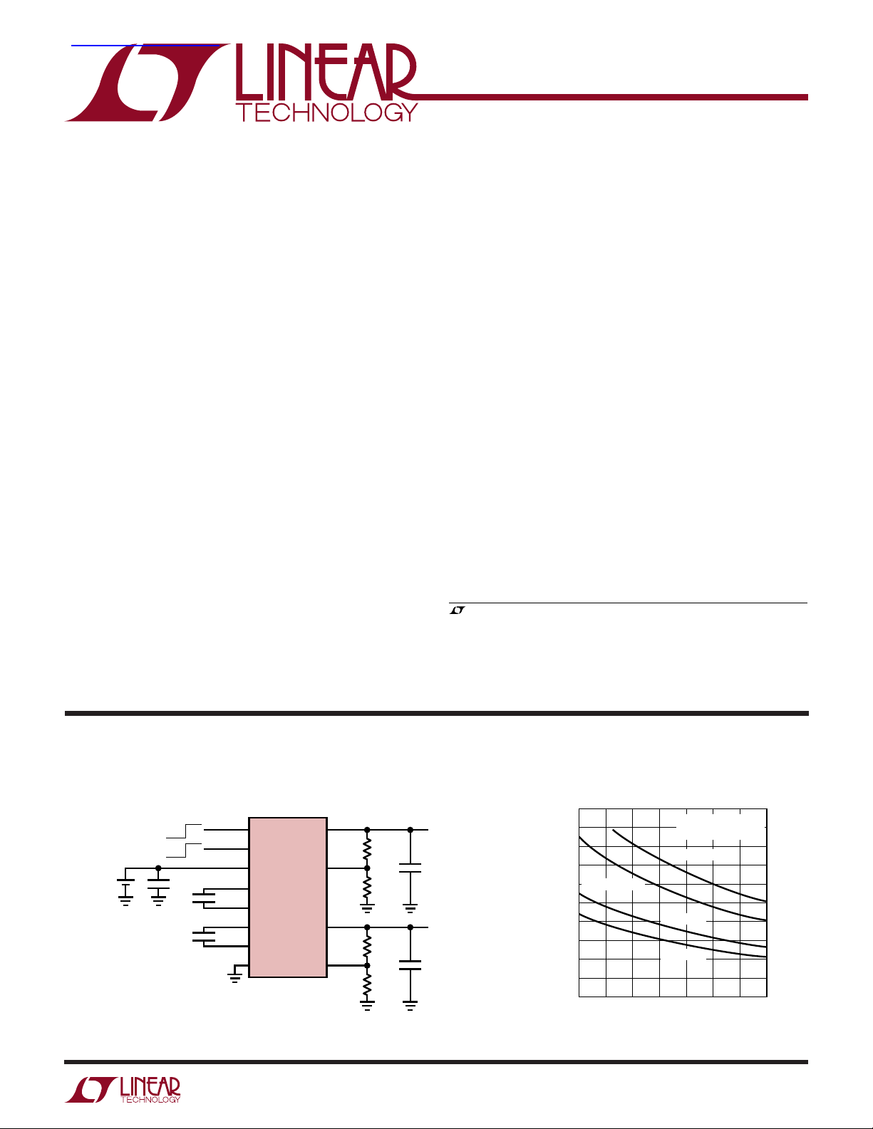
TYPICAL APPLICATIO
1.5V and 1.2V Output Voltages with Shutdown
2
1µF
1µF
EN1
11
EN2
3
V
IN
4
+
C1
6
–
C1
10
+
C2
8
–
C2
7
GND
1-CELL
Li-ION
OR 3-CELL
NiMH
OFF ON
OFF ON
4.7µF
U
LTC3252
OUT1
FB1
OUT2
FB2
1.5V/1.2V Efficiency vs Input Voltage
5
470k
1
510k
9
261k
12
510k
V
I
OUT
4.7µF
V
I
OUT
4.7µF
= 1.5V
OUT
≤ 250mA
= 1.2V
OUT
≤ 250mA
3252 TA01
100
90
80
70
60
LTC3252-1.2V
50
40
EFFICIENCY (%)
30
20
10
0
3.1 3.5 3.9 4.3 4.7 5.1 5.5
2.7
I
(1.5V) = 100mA
OUT
(1.2V) = 100mA
I
OUT
LTC3252-1.5V
LDO-1.5V
LDO-1.2V
VIN (V)
3252 TA01a
3252f
1
LTC3252
FB2
EN2
C2
+
OUT2
C2
–
GND
FB1
EN1
V
IN
C1
+
OUT1
C1
–
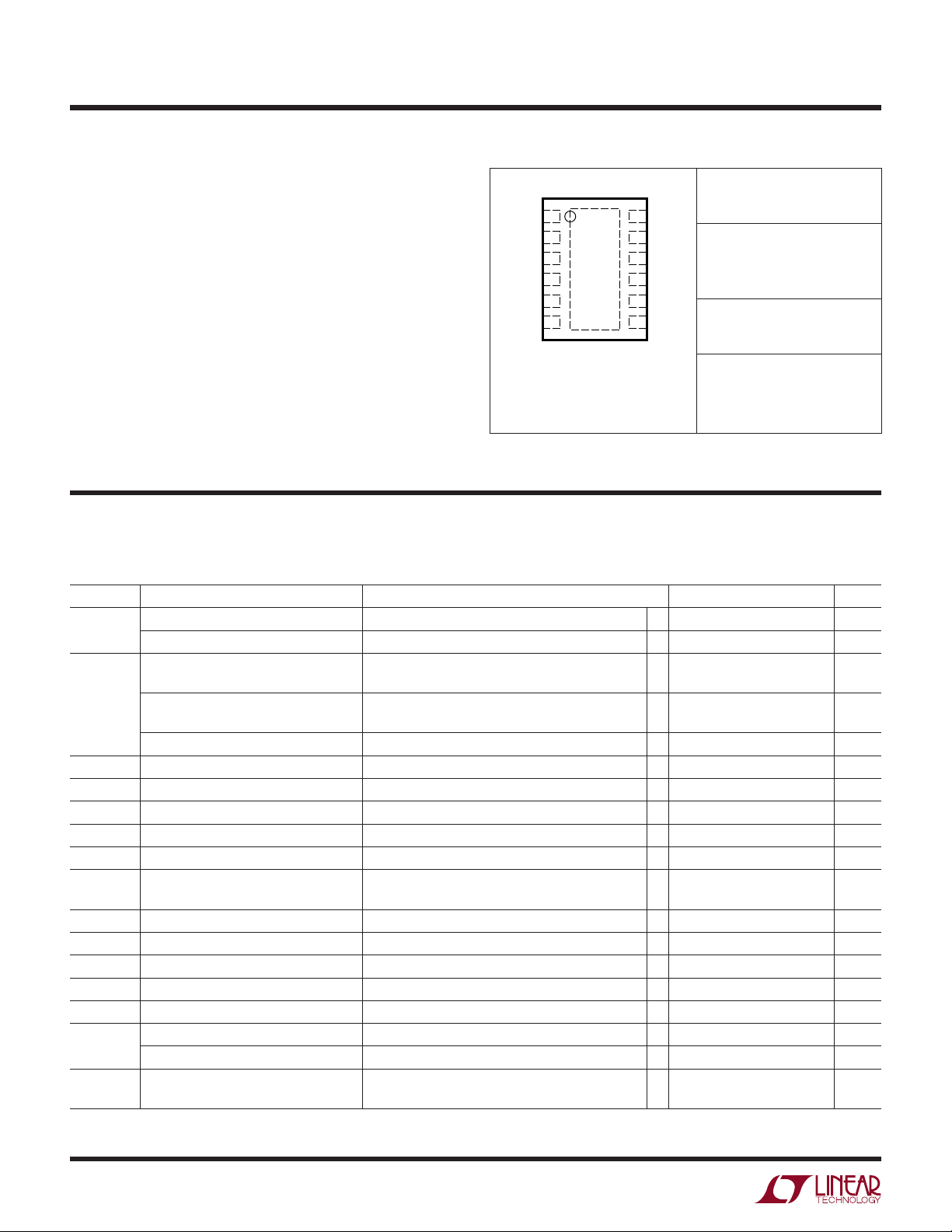
TOP VIEW
DE PACKAGE
12-LEAD (4mm × 3mm) PLASTIC DFN
12
11
10
9
8
7
1
2
3
4
5
6
WW
W
ABSOLUTE AXI U RATI GS
U
PACKAGE/ORDER I FOR ATIO
(Notes 1, 6)
VIN to GND................................................–0.3V to 6.0V
EN1, EN2, FB1, FB2 to GND .......... –0.3V to (VIN + 0.3V)
I
, I
OUT1
(Note 3)........................................... 400mA
OUT2
Operating Ambient Temperature Range
(Note 2) .................................................. – 40°C to 85°C
Storage Temperature Range ................. –65°C to 125°C
Lead Temperature (Soldering, 10 sec).................. 300°C
T
JMAX
Consult LTC Marketing for parts specified with wider operating temperature ranges.
ELECTRICAL CHARACTERISTICS
temperature range, otherwise specifications are at TA = 25°C. VIN = 3.6V, V
4.7µF (all capacitors ceramic) unless otherwise noted.
The ● denotes the specifications which apply over the full operating
EXPOSED PAD IS GROUND
(MUST BE SOLDERED TO PCB)
= 125°C, θJA = 40°C/W, θJC = 4.3°C/W
OUT1
= V
= 1.5V, C1 = C2 = 1µF, Cin = C
OUT2
UUW
ORDER PART
NUMBER
LTC3252EDE
DE PART
MARKING
3252
OUT1
= C
OUT2
=
SYMBOL PARAMETER CONDITIONS MIN TYP MAX UNITS
V
IN
Min Operating Voltage (Note 4) ● 2.7 V
Max Operating Voltage ● 5.5 V
I
VIN
Operating Current, I
Both Outputs Enabled 2.7V ≤ V
Operating Current, I
One Output Enabled V
Shutdown Current VM0 = 0V, VM1 = 0V, 2.7V ≤ VIN ≤ 5.5V ● 0.01 1 µA
V
FB1
I
OUT1
I
OUT2
I
FB
V
RIPPLE
, V
Feedback Voltage I
FB2
Output Current V
Output Current V
FB1, FB2 Input Current V
Output Ripple (OUT1 or OUT2) I
Spread Spectrum Frequency Range f
V
IH
V
IL
I
IH
I
IL
t
ON
OUT1, OUT2 Load Regulation (Referred to FB pin) 0.08 mV/mA
R
OL
2
EN1, EN2 Input High Voltage 2.7V ≤ VIN ≤ 5.5V ● 1.2 0.8 V
EN1, EN2 Input Low Voltage 2.7V ≤ VIN ≤ 5.5V ● 0.8 0.4 V
EN1, EN2 Input High Current EN1 = VIN, EN2 = V
EN1, EN2 Input Low Current EN1 = 0V, EN2 = 0V ● –1 1 µA
Turn On Time R
Line Regulation 0 ≤ I
Open Loop Output Impedance, VIN = 3.0V, I
(OUT1 or OUT2)
= 0mA, V
OUT
= 0mA, V
OUT
= 0, 2.7V ≤ V
EN2
= 0mA, 2.7V ≤ V
OUT
= V
EN1
= V
EN2
= V
FB1
FB2
= 250mA 10 mV
OUT
Switching Frequency ● 0.8 1.0 MHz
MIN
Switching Frequency ● 1.6 2.0 MHz
f
MAX
= 3Ω 0.8 ms
OUT
OUT1
IN
IN
IN
EN1
≤ 5.5V
EN1
= VIN, V
= 0, V
IN
= VIN, ● 60 100 µA
EN2
= VIN or V
EN2
= VIN, ● 35 60 µA
EN1
≤ 5.5V
≤ 5.5V ● 0.78 0.8 0.82 V
IN
● 250 mA
● 250 mA
= 0.85V ● –50 50 nA
IN
≤ 250mA or 0 ≤ I
= 200mA, VFB = 0.74V (Note 5) ● 1 1.4 Ω
OUT
≤ 250mA 0.2 %/V
OUT2
● –1 1 µA
P-P
3252f
ELECTRICAL CHARACTERISTICS
LTC3252
Note 1: Absolute Maximum Ratings are those values beyond which the life
of a device may be impaired.
Note 2: The LTC3252EDE is guaranteed to meet specified performance
from 0°C to 70°C. Specifications over the –40°C and 85°C operating
temperature range are assured by design characterization and correlation
with statistical process control.
Note 3: Based on long-term current density limitations.
Note 4: Minimum operating voltage required for regulation is:
> 2 • (V
V
IN
Note 5: Output not in regulation; R
Note 6: This IC includes overtemperature protection that is intended to
protect the device during momentary overload conditions. Junction
temperature will exceed 125°C when overtemperature protection is active.
Continuous operation above the specified maximum operating junction
temperature may impair device reliability.
UW
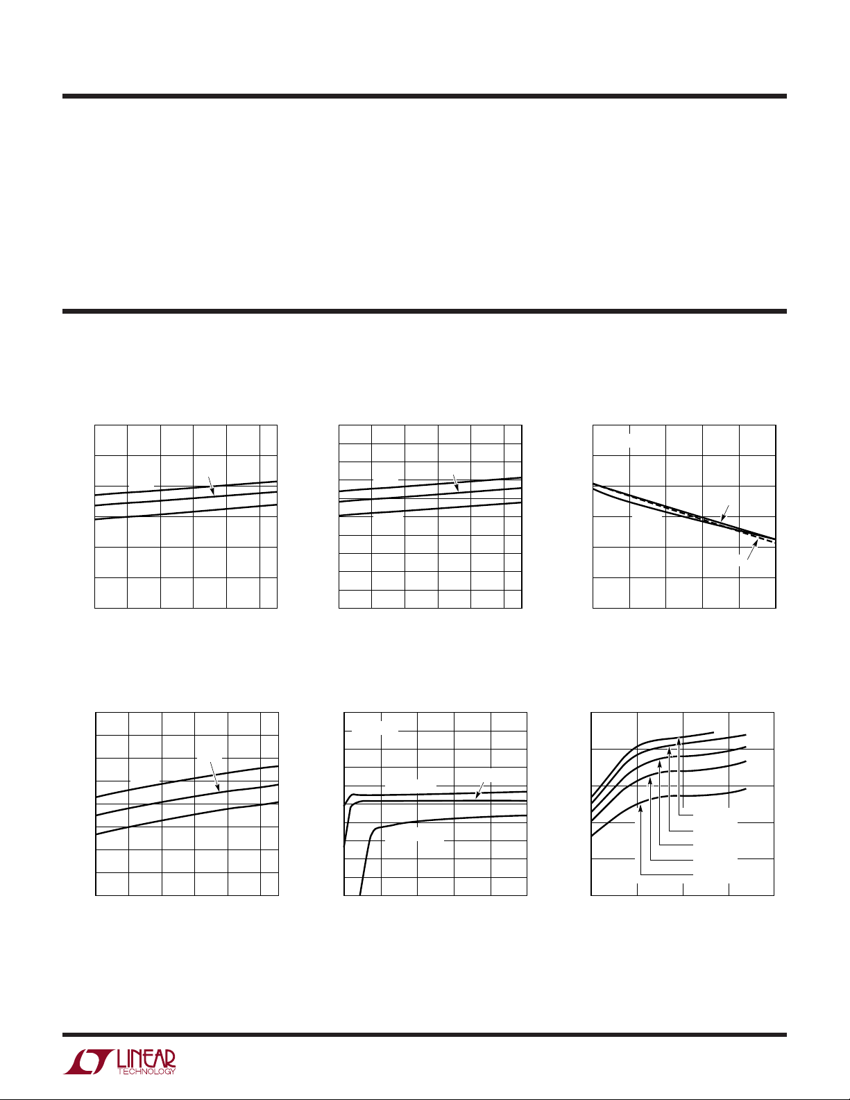
TYPICAL PERFOR A CE CHARACTERISTICS
No Load Supply Current vs Supply
Voltage (One Output Enabled)
60
50
40
30
(µA)
IN
I
20
10
0
2.7
85°C
–45°C
3.7 4.2 4.7
3.2
25°C
VIN (V)
5.2
3252 G01
No Load Supply Current vs Supply
Voltage (Both Outputs Enabled)
100
90
80
70
60
(µA)
50
CC
I
40
30
20
10
0
2.7
85°C
–40°C
3.7 4.2 4.7
3.2
25°C
VIN (V)
OUT(MIN)
5.2
3252 G02
+ ROL • I
0.82
0.81
0.80
(V)
0.79
FB
V
0.78
0.77
0.76
)
OUT
= (VIN/2 – V
OL
OUT
)/I
OUT
.
FB Voltage vs Load Current
VIN = 3.6V
25°C
–40°C
85°C
50 100 150 200 250
0
I
(mA)
OUT
3252 G03
EN1/EN2 Input Threshold Voltage
vs Supply Voltage
1.2
1.1
25°C
VIN (V)
(V)
SHDN
V
1.0
0.9
0.8
0.7
0.6
0.5
0.4
2.7
–40°C
85°C
3.7 4.2 4.7
3.2
5.2
3252 G04
1.5V Output Voltage vs Supply
Voltage
1.60
TA = 25°C
1.58
1.56
1.54
I
(V)
OUT
V
1.52
1.50
1.48
1.46
1.44
1.42
1.40
3
= 0mA
OUT
I
= 250mA
OUT
3.5 4 4.5 5 5.5
VIN (V)
I
OUT
= 50mA
3252 G05
1.5V Output Efficiency vs Output
Current
100
= 25°C
T
A
80
60
I
OUT
VIN = 3.1V
V
V
V
V
(mA)
= 3.3V
IN
= 3.6V
IN
= 4V
IN
= 5V
IN
40
EFFICIENCY (%)
20
0
0.1
1 10 100 1000
3252 G06
3252f
3
LTC3252
UW
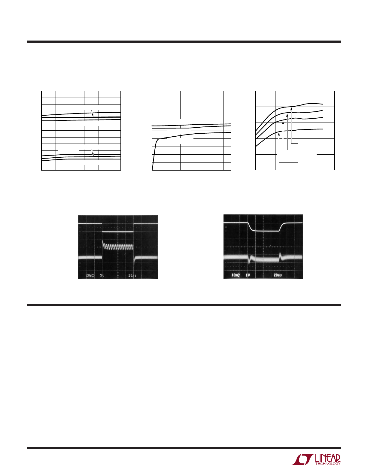
TYPICAL PERFOR A CE CHARACTERISTICS
Oscillator Max/Min Frequency vs
Supply Voltage
2.0
1.9
1.8
1.7
1.6
1.5
1.4
1.3
1.2
FREQUENCY (MHz)
1.1
1.0
0.9
0.8
2.7
–40°C MAX
3.2
–40°C MIN
25°C MAX
85°C MAX
25°C MIN
85°C MIN
3.7 4.2 4.7
VIN (V)
Output Current Transient
Response
250mA
I
OUT
20mA
V
OUT
20mV/DIV
AC
5.2
3252 G07
1.2V Output Voltage vs Supply
Voltage 1.2V Efficiency vs Load Current
100
TA = 25°C
80
60
40
EFFICIENCY (%)
20
0
0.1
VIN = 2.8V
V
V
V
1 10 100 1000
I
(mA)
OUT
(V)
OUT
V
1.30
1.28
1.26
1.24
1.22
1.20
1.18
1.16
1.14
1.12
1.10
2.7
TA = 25°C
3.2
I
= 0mA
OUT
I
= 50mA
OUT
I
= 250mA
OUT
3.7 4.2 4.7
VIN (V)
5.2
3252 G08
Line Transient Response
4.5V
V
IN
3.5V
V
OUT
10mV/DIV
AC
= 3.1V
IN
= 3.5V
IN
= 4.5V
IN
3252 G09
VIN = 3.6V
V
= 1.5V
OUT
3252 G11
UUU
PI FU CTIO S
FB1 (Pin 1): Feedback Input Pin 1. An output divider
should be connected from OUT1 to FB1 to program the
output voltage.
EN1 (Pin 2): Input Enable Pin 1. When EN1 is high, OUT1
is enabled. When EN1 is low OUT1 is shut down.
VIN (Pin 3): Input Supply Voltage. Operating VIN may be
between 2.7V and 5.5V. Bypass VIN with a ≥ 4.7µF (1µF
min) low ESR ceramic capacitor to GND (CIN).
V
I
OUT
OUT
= 1.5V
= 150mA
3252 G12
C1+ (Pin 4): Flying Capacitor 1 Positive Terminal (C1).
OUT1 (Pin 5): Regulated Output Voltage 1. OUT1 is
disconnected from VIN when in shutdown. Bypass OUT1
with a low ESR ceramic capacitor to GND (CO1). See
Output Capacitor Selection section for size requirements.
C1– (Pin 6): Flying Capacitor 1 Negative Terminal (C1).
GND (Pin 7): Ground. Connect to a ground plane for best
performance.
3252f
4
 Loading...