

FEATURES
■
Charge Pump Provides High Efficiency with
Automatic Mode Switching
■
Multimode Operation: 1x, 1.5x, 2x
■
Four Low Dropout LED Outputs
■
Up to 600mA Total Output Current
■
Independent Torch and Flash I
■
Low Noise Constant Frequency Operation*
■
PWM Brightness Control via the EN2 Pin
■
Low Shutdown Current: 4µA
■
Internal Soft-Start Limits Inrush Current During
and Enable Pins
SET
Start-Up and Mode Switching
■
Open/Short LED Protection
■
No Inductors
■
(3mm x 3mm) 16-Lead QFN Plastic Package
U
APPLICATIO S
■
Multi-LED Camera Light Supply for Cellphones/
DSCs/PDAs
, LTC and LT are registered trademarks of Linear Technology Corporation.
All other trademarks are the property of their respective owners.
*Protected by U.S. Patents, including 6411531
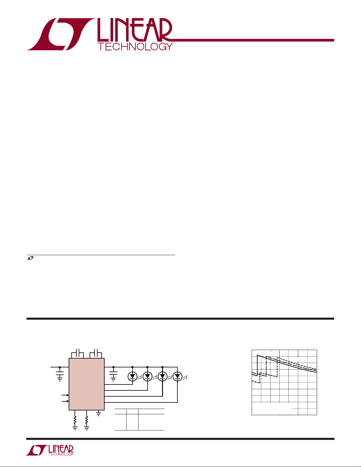
LTC3217
600mA Low Noise
Multi-LED Camera Light
Charge Pump
U
DESCRIPTIO
The LTC®3217 is a low noise charge pump DC/DC converter designed to power four high current LEDs. The
LTC3217 requires only four small ceramic capacitors and
two current set resistors to form a complete LED power
supply and current controller.
Built-in soft-start circuitry prevents excessive inrush current during start-up and mode changes. High switching
frequency enables the use of small external capacitors.
Independent high and low current settings are programmed
by two external resistors. Shutdown mode and current
output levels are selected via two logic inputs.
The current through the LEDs is programmed via I
I
. In addition, the brightness can be controlled by
SET2
pulse width modulation of the EN2 pin.
The charge pump optimizes efficiency based on the voltage across the LED current sources. The part powers up
in 1x mode and will automatically switch to boost mode
whenever any enabled LED current source begins to enter
dropout. The first dropout switches the part into 1.5x
mode and a subsequent dropout switches the part into 2x
mode. The LTC3217 resets to 1x mode whenever the part
is shut down.
SET1
and
TYPICAL APPLICATIO
C2
2.2µFC32.2µF
C1P C1M C2P C2M
V
BAT
C1
2.2µF
EN1 (TORCH)
EN2 (FLASH)
19.6k
V
EN1
EN2
1%
BAT
I
SET1ISET2
LTC3217
6.49k
1%
CPO
LED1
LED2
LED3
LED4
GND
C4
2.2µF
EN1
0
1
0
1
U
EN2 I
0
0 (SHUTDOWN)
0
25mA/LED
1
75mA/LED
1
100mA/LED
LED
The LTC3217 is available in a low profile 16-lead (3mm ×
3mm × 0.75mm) QFN package.
3217 TA01
AOT-2015HPW-1751B
100
100mA
90
80
70
/PIN) (%)
60
LED
50
40
30
EFFICIENCY (P
20
TOTAL OUTPUT CURRENT
10
/PIN
P
LED
LED = 2015 HPW AOT
0
3
3.2
Efficiency vs V
200mA
3.6
3.4
V
BAT
(V)
3.8
BAT
400mA
4
4.4
4.2
3217 G09
3217f
1

LTC3217
16 15 14 13
5 6 7 8
TOP VIEW
17
UD PACKAGE
16-LEAD (3mm × 3mm) PLASTIC QFN
9
10
11
12
4
3
2
1C1P
CPO
EN1
LED1
C2M
EN2
I
SET2
I
SET1
C2P
V
BAT
C1M
GND1
LED2
LED3
LED4
GND2
WW
W
U
ABSOLUTE AXI U RATI GS
(Note 1)
V
, CPO to GND ....................................... –0.3V to 6V
BAT
EN1, EN2 .................................... –0.3V to (V
(Note 2) ....................................................... 600mA
I
CPO
I
(Note 3) .................................................. 150mA
ILED1-4
CPO Short-Circuit Duration ............................. Indefinite
Operating Temperature Range (Note 4) ... –40°C to 85°C
Storage Temperature Range ..................–65°C to 125°C
BAT
+ 0.3V)
UUW
PACKAGE/ORDER I FOR ATIO
T
= 125°C, θJA = 68°C/W
EXPOSED PAD (PIN 17) IS GND MUST BE SOLDERED TO PCB
ORDER PART NUMBER
LTC3217EUD
Order Options Tape and Reel: Add #TR
Lead Free: Add #PBF Lead Free Tape and Reel: Add #TRPBF
Lead Free Part Marking: http://www.linear.com/leadfree/
Consult LTC Marketing for parts specified with wider operating temperature ranges.
JMAX
QFN PART MARKING
LBTQ
ELECTRICAL CHARACTERISTICS
temperature range, otherwise specifications are at T
PARAMETER CONDITIONS MIN TYP MAX UNITS
V
Operating Voltage
BAT
I
Operating Current R
VBAT
V
Shutdown Current 4 µA
BAT
LED 1-4 Current
LED Current Ratio (I
LED Dropout Voltage Mode Switch Threshold, I
Mode Switching Delay EN1 Only 2.5 ms
LED Current Matching Any Two Outputs, I
Charge Pump (CPO)
1x Mode Output Voltage I
1.5x Mode Output Voltage I
2x Mode Output Voltage I
1x Mode Output Impedance 0.5 Ω
1.5x Mode Output Impedance V
2x Mode Output Impedance V
CLOCK Frequency
LED/ISET1/2
)I
The ● denotes the specifications which apply over the full operating
= 25°C. V
A
ISET1
I
CPO
I
CPO
I
CPO
LED
CPO
CPO
CPO
BAT
BAT
= 3.6V, C1 = C2 = C3 = C4 = 2.2µF, unless otherwise noted.
BAT
●
2.9 4.5 V
= R
= 20k, EN1 = EN2 = High
ISET2
= 0mA, 1x Mode 1 mA
= 0mA, 1.5x Mode 4 mA
= 0mA, 2x Mode 6 mA
= 25mA to 100mA
= 100mA 330 mV
LED
= 100mA 1 %
LED
= 0mA V
= 0mA 4.5 V
= 0mA 5.05 V
= 3.4V, V
= 3.2V, V
≤ 4.6V (Note 5) 2.8 Ω
CPO
≤ 5.1V (Note 5) 3.2 Ω
CPO
●
370 400 430 mA/mA
BAT
●
0.6 0.85 1.15 MHz
V
3217f
2
LTC3217
R
ISET
(kΩ)
0
I
LED
(mA)
40
80
120
20
60
100
10 20 30 40
3217 G03
505015253545
ELECTRICAL CHARACTERISTICS
temperature range, otherwise specifications are at T
The ● denotes the specifications which apply over the full operating
= 25°C. V
A
= 3.6V, C1 = C2 = C3 = C4 = 2.2µF, unless otherwise noted.
BAT
PARAMETER CONDITIONS MIN TYP MAX UNITS
EN1, EN2
Low Level Input Voltage (VIL)
High Level Input Voltage (VIH)
Input Current (IIH)
Input Current (IIL)
Minimum PWM On-Time EN2 Only
Maximum PWM Off-Time EN2 to Remain Enabled, EN1 = Low
I
, I
SET1
SET2
V
ISET1, ISET2
I
ISET1, ISET2
I
ISET1, ISET2
Current Range
Short-Circuit Current 800 µA
Note 1: Absolute Maximum Ratings are those values beyond which the life of
a device may become impaired.
Note 2: Based on charge pump long-term current density limitations.
Assumes an operating duty cycle of ≤ 10% under absolute maximum
conditions for durations less than 10 seconds. Maximum current for
continuous operation is 300mA.
Note 3: Based on LED current source long-term current density limitations.
Assumes an operating duty cycle of ≤ 10% under absolute maximum
I
LED1-4
= 12.5mA
conditions for durations less than 10 seconds. Maximum current for
continuous operation is 100mA.
Note 4: The LTC3217E is guaranteed to meet performance specifications
from 0°C to 70°C. Specifications over the –40°C to 85°C ambient operating
temperature range are assured by design, characterization and correlation
with statistical process controls.
Note 5: 1.5x mode output impedance is defined as (1.5V
2x mode output impedance is defined as (2V
●
●
1.4 V
●
730µA
●
–1 1 µA
●
50 µs
●
●
1.175 1.215 1.255 V
●
31.25 375 µA
– V
BAT
CPO
BAT
)/I
0.4 V
1ms
– V
CPO
.
OUT
)/I
.
OUT
UW
TYPICAL PERFOR A CE CHARACTERISTICS
LED Dropout Voltage
vs LED Current
400
V
= 3.6V
BAT
300
200
100
LED DROPOUT VOLTAGE (mV)
0
10
20 30 40 50
LED CURRENT (mA)
60 70 80 90 100
3217 G01
LED Pin Current
vs LED Pin Voltage
120
V
= 3.6V
BAT
100
80
60
40
LED PIN CURRENT (mA)
20
0
0
0.2 0.4 0.6 0.8
LED PIN VOLTAGE (V)
TA = 25°C unless otherwise noted.
vs R
I
LED
1.0
3217 G02
ISET
3217f
3
LTC3217
V
BAT
(V)
3
0
EFFICIENCY (P
LED
/PIN) (%)
10
30
40
50
100
70
3.4
3.8
4
3217 G09
20
80
90
60
3.2
3.6
4.2
4.4
TOTAL OUTPUT CURRENT
P
LED
/PIN
LED = 2015 HPW AOT
100mA
200mA
400mA
UW
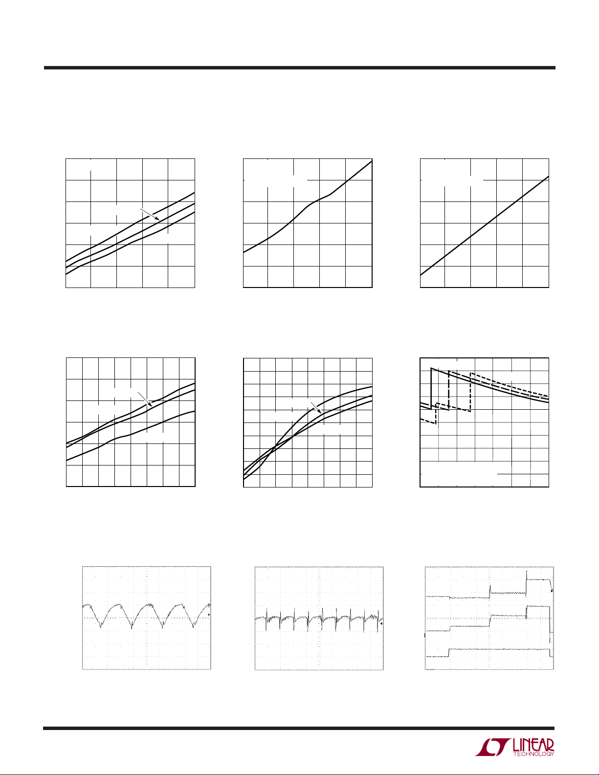
TYPICAL PERFOR A CE CHARACTERISTICS
TA = 25°C unless otherwise noted.
1x Mode Switch Resistance
vs Temperature
0.65
I
= 200mA
CPO
0.60
SWITCH RESISTANCE (Ω)
0.55
0.50
0.45
0.40
0.35
SHUTDOWN CURRENT (µA)
BAT
V
7.5
6.5
5.5
4.5
3.5
2.5
1.5
–40
2.9
V
BAT
vs V
V
= 3.6V
BAT
V
= 3.3V
BAT
–15 10 35 60
TEMPERATURE (°C)
Shutdown Current
Voltage
BAT
TA = –40°C
TA = 85°C
3.3 3.7
3.1 3.5
V
VOLTAGE (V)
BAT
V
BAT
TA = 25°C
4.1
3.9
= 3.9V
4.3
3217 G04
3217 G07
85
4.5
1.5x Mode Charge Pump Open-Loop
Output Resistance vs Temperature
(1.5V
3.2
3.0
2.8
2.6
2.4
SWITCH RESISTANCE (Ω)
2.2
2.0
–40
– V
BAT
V
= 3V
BAT
= 4.2V
V
CPO
C2 = C3 = C4 = 2.2µF
–15 10 35 60
)/I
CPO
TEMPERATURE (°C)
CPO
Oscillator Frequency
vs Supply Voltage
980
970
960
950
940
930
920
FREQUENCY (kHz)
910
900
890
880
2.9
TA = 25°C
TA = –40°C
3.1 3.5
3.3
V
SUPPLY VOLTAGE (V)
BAT
3.7
TA = 85°C
3.9
4.1
4.3
3217 G05
3217 G08
85
4.5
2x Mode Charge Pump Open-Loop
Output Resistance vs Temperature
(2V
– V
BAT
3.8
V
BAT
V
CPO
3.6
C2 = C3 = C4 = 2.2µF
3.4
3.2
3.0
SWITCH RESISTANCE (Ω)
2.8
2.6
–40
Efficiency vs V
= 3V
= 4.8V
–15 10 35 60
)/I
CPO
CPO
TEMPERATURE (°C)
BAT
85
3217 G06
AC COUPLED
4
V
CPO
50mV/DIV
1.5x Mode CPO Output Ripple 2x Mode CPO Output Ripple
V
CPO
20mV/DIV
3217 G10
AC COUPLED
V
I
C
BAT
CPO
CPO
= 3.6V
= 400mA
= 2.2µF
500ns/DIV
I
C
BAT
CPO
CPO
= 3.6V
= 400mA
= 2.2µF
500ns/DIVV
3217 G11
V
CPO
1V/DIV
I
VBAT
500mA/DIV
EN1
5V/DIV
Charge Pump Mode Switching
and Input Current to Ground
(400mA Load)
0
V
1x
NO LOAD
= 3.6V
IN
1x
DROPOUT
1.5x
DROPOUT
1ms/DIV
2x
(5V)
3217 G12
3217f

UW
TYPICAL PERFOR A CE CHARACTERISTICS
LTC3217
TA = 25°C unless otherwise noted.
1.5x Mode CPO Voltage
vs Load Current
4.8
C2 = C3 = C4 = 2.2µF
4.6
3.4V
3.5V
3.6V
5000
3217 G13
U
4.4
4.2
4.0
CPO VOLTAGE (V)
3.8
3.6
3.3V
100 200 300 400
UU
3.2V
3.1V
V
= 3V
BAT
LOAD CURRENT (mA)
PI FU CTIO S
C1P, C2P, C1M, C2M (Pins 1, 16, 14, 12): Charge Pump
Flying Capacitor Pins. A 2.2µF X7R or X5R ceramic capaci-
tor should be connected from C1P to C1M and C2P to C2M.
CPO (Pin 2): Output of the charge pump used to power all
LEDs. This pin is enabled or disabled using the EN1 and
EN2 inputs. A 2.2µF X5R or X7R ceramic capacitor should
be connected to ground.
EN1, EN2 (Pins 3, 11): Inputs. The EN1 and EN2 pins are
used to select which current level is being supplied to the
LEDs, as well as to put the part into shutdown mode. The
truth table for these pins is as follows:
Truth Table
EN1 EN2 MODE
0 0 Shutdown
1 0 Low Current
0 1 High Current
1 1 Low + High Current
2x Mode CPO Voltage
vs Load Current
5.2
C2 = C3 = C4 = 2.2µF
5.1
5.0
4.9
4.8
4.7
4.6
CPO VOLTAGE (V)
4.5
4.4
4.3
4.2
100
0
3.3V
300
200
LOAD CURRENT (mA)
3.2V
V
BAT
3.1V
= 3V
400
3.6V
500
3217 G14
current to each LED output is set via the EN1 and EN2
inputs, and the programming resistors connected from
I
SET1
and I
to GND. Any of the four LED outputs can
SET2
be disabled by connecting the output directly to CPO.
10µA of current will flow through each directly connected
LED output. For single LED applications, all four LED pins
may be tied together and will accurately share current.
GND2 (Pin 8): Analog Ground. This pin should be
connected directly to a low impedance ground plane.
I
SET1/ISET2
Resistor Pins. The I
(Pins 9, 10): LED Current Programming
SET1
and I
pins will servo to 1.22V.
SET2
Resistors connected between each of these pins and GND
are used to set the high and low LED current levels.
Connecting a resistor 2k or less will cause the LTC3217 to
enter over-current shutdown.
GND1 (Pin 13): Charge Pump Ground. This pin should be
connected directly to a low impedance ground plane.
EN2 can be used for PWM of the LED currents. For proper
operation, the minimum pulse width should be 50µs and
the maximum low time should be 1ms if EN1 is low. If EN1
is high then the 1ms low time limitation does not apply.
LED1, LED2, LED3, LED4 (Pins 4, 5, 6, 7): LED1 to LED4
are the current source outputs. Each LED is connected in
between CPO (anodes) and LED1 – 4 (cathodes). The
(Pin 15): Supply Voltage. This pin should be
V
BAT
bypassed with a 2.2µF, or greater low ESR ceramic
capacitor.
Exposed Pad (Pin 17): This pad should be connected
directly to a low impedance ground plane for optimal
thermal and electrical performance.
3217f
5

LTC3217
BLOCK DIAGRA
W
1
C1P
850kHz
OSCILLATOR
V
BAT
15
14 16 12
C1M C2P C2M
CHARGE PUMP
GND1
CPO
13
2
–
+
ENABLE CP
+
CPO
+
I
SET1
9
MUX
I
SET2
10
–
1.22V
LED CURRENT
SOURCES
4
SHORT-CIRCUIT
PROTECTION
–
+
–
0.8V
LED1
LED2
LED3
LED4
4
5
6
7
EN1
3
250k
EN2
11
250k
PWM TIMING
CONTROL LOGIC
U
OPERATIO
Power Management
The LTC3217 uses a switched capacitor charge pump to
boost CPO to as much as 2 times the input voltage up to
5.1V. The part starts up in 1x mode. In this mode, V
connected directly to CPO. This mode provides maximum
efficiency and minimum noise. The LTC3217 will remain
in 1x mode until an LED current source drops out. Dropout
occurs when a current source voltage becomes too low
for the programmed current to be supplied. When dropout
is detected, the LTC3217 will switch into 1.5x mode. The
CPO voltage will then start to increase and will attempt to
reach 1.5x V
up to 4.5V. Any subsequent dropout will
BAT
BAT
is
GND2
8
THERMAL
SHUTDOWN
3217 BD
cause the part to enter the 2x mode. The CPO voltage will
attempt to reach 2x V
up to 5.05V. The LTC3217 will be
BAT
reset to 1x mode whenever the part is shut down.
A two phase non-overlapping clock activates the charge
pump switches. In the 2x mode the flying capacitors are
charged on alternate clock phases from V
to minimize
BAT
input current ripple and CPO voltage ripple. In 1.5x mode
the flying capacitors are charged in series during the first
clock phase and stacked in parallel on V
during the
BAT
second phase. This sequence of charging and discharging
the flying capacitors continues at a constant frequency
of 850kHz.
3217f
6

OPERATIO
I
VV
R
OUT
BAT CPO
OL
=
15.–
LTC3217
U
The LED currents are delivered by the four programmable
current sources. Three discrete current settings (Low, High,
Low + High) are available and may be selected via the EN1 and
EN2 pins. The values of these currents may be selected by
choosing the appropriate programming resistors. Each resistor is connected between the I
SET1
or I
pin to ground.
SET2
The resistor values required to attain the desired current
levels can be determined by Equation 1.
R
An R
SET
SETx
488
12
/
=
I
LEDx
(1)
resistor value of 2k or less (i.e., short-circuit) will
cause the LTC3217 to enter overcurrent shutdown mode.
This mode prevents damage to the part and external LEDs by
shutting down the high power sections of the part.
Each LED output can be disabled by connecting the pin
directly to CPO. Do not leave pins open as this will cause
dropout and subsequently mode changing.
Pulse Width Modulation Option
can be pulse width modulated to control the
EN2
LED brightness. The minimum allowable pulse width is 50µs
and the maximum low time is 1ms. Pulse width modulating
the EN2 input can be performed with EN1 high or low. If EN1
is high then there is no limitation on the EN2 low time. When
EN1 is low the part would normally go into shutdown
whenever EN2 goes low. Prevention of shutdown in this case
is achieved by an internal timer which delays shutdown until
EN2 has remained low for at least 1ms.
Charge Pump Strength and Regulation
Regulation is achieved by sensing the voltage at the CPO pin
and modulating the charge pump strength based on the error
signal. The CPO regulation voltages are set internally, and are
dependent on the charge pump modes as shown in Table 1.
When the LTC3217 operates in either 1.5x mode or 2x mode,
the charge pump can be modeled as a Thevenin-equivalent
circuit to determine the amount of current available from the
effective input voltage and effective open-loop output resistance, R
Table 1. Charge Pump Output Regulation Voltages
(Figure 1).
OL
CHARGE PUMP MODE REGULATED V
1.5x 4.5V
2x 5.05V
CPO
ROL is dependent on a number of factors including the
switching term, 1/(2f
OSC
• C
), internal switch resis-
FLY
tances and the non-overlap period of the switching circuit.
However, for a given R
, the amount of current available
OL
will be directly proportional to the advantage voltage of
1.5V
BAT
– V
for 1.5x mode and 2V
CPO
BAT
– V
CPO
for 2x
mode. Consider the example of driving white LEDs from
a 3.1V supply. If the LED forward voltage is 3.8V and the
current sources require 100mV, the advantage voltage for
1.5x mode is 3.1V • 1.5 - 3.8V – 0.1V or 750mV. Notice
that if the input voltage is raised to 3.2V, the advantage
voltage jumps to 900mV—a 20% improvement in available strength.
From Figure 1, for 1.5x mode the available current is given by:
Soft-Start
Initially, when the part is in shutdown, a weak switch connects V
to CPO. This allows V
BAT
to slowly charge the CPO
BAT
output capacitor and prevent large charging currents to
occur.
The LTC3217 also employs a soft-start feature on its charge
pump to prevent excessive inrush current and supply droop
when switching into the step-up modes. The current available
to the CPO pin is increased linearly over a typical period of
125µs. Soft-start occurs at the start of both 1.5x and 2x
mode changes.
(2)
For 2x mode, the available current is given by:
VV
2–
I
OUT
=
BAT CPO
R
OL
(3)
Notice that the advantage voltage in this case is
3.1V • 2 – 3.8V – 0.1V = 2.3V. R
is higher in 2x mode
OL
but a significant overall increase in available current
is achieved.
3217f
7

LTC3217
OPERATIO
U
R
OL
+
–
BAT
OR 2V
BAT
+
CPO1.5V
–
3217 F01
Figure 1. Equivalent Open-Loop Circuit
V
in calculating Equations 2 and 3 is the minimum
CPO
required voltage for the LED and not the regulated voltage.
Typical values of R
as a function of temperature are shown
OL
in Figures 2 and 3.
3.2
V
= 3V
BAT
= 4.2V
V
CPO
3.0
C2 = C3 = C4 = 2.2µF
2.8
2.6
2.4
SWITCH RESISTANCE (Ω)
2.2
Shutdown Current
In shutdown mode all the circuitry is turned off and the
LTC3217 draws a very low current from the V
Furthermore, CPO is weakly connected to V
BAT
BAT
supply.
. The
LTC3217 enters shutdown mode when both the EN1 and
EN2 pins are brought low. EN1 and EN2 have 250k pulldown resistors to ground.
Thermal Protection
The LTC3217 has built-in overtemperature protection. At
internal die temperatures of around 150°C thermal shutdown will occur. This will disable all of the current sources
and charge pump until the die has cooled by about 15°C.
This thermal cycling will continue until the fault has
been corrected.
CPO Short-Circuit Protection
The LTC3217 has internal CPO short-circuit protection. An
internal comparator senses when CPO is below 0.8V
which forces the part into shutdown. A pull-up device
ensures start-up.
2.0
–40
–15 10 35 60
TEMPERATURE (°C)
85
3217 G05
Figure 2. 1.5x Mode Charge Pump Open-Loop Output
Resistance vs Temperature (1.5V
3.8
V
= 3V
BAT
= 4.8V
V
CPO
3.6
C2 = C3 = C4 = 2.2µF
3.4
3.2
3.0
SWITCH RESISTANCE (Ω)
2.8
2.6
–40
–15 10 35 60
TEMPERATURE (°C)
BAT
– V
CPO
3217 G06
)/I
CPO
85
Figure 3. 2x Mode Charge Pump Open-Loop Output
Resistance vs Temperature (2V
BAT
– V
CPO
)/I
CPO
Mode Switching
The LTC3217 will automatically switch from 1x mode to
1.5x mode and subsequently to 2x mode whenever a
dropout condition is detected at an LED pin. Dropout
occurs when a current source voltage becomes too low for
the programmed current to be supplied. The time from
dropout detection and mode switching is about 2.5ms.
This delay allows for the LED to warm up and reduce its
forward voltage which may remove the dropout condition.
If PWM is used on the EN2 pin, then the dropout time is
dependent on one to two PWM clock pulses.
The part is reset back to 1x mode when the part is shut
down (EN1 = EN2 = Low). The part may be set to the
desired output current level via EN1 and EN2. An internal
comparator will not allow the main switches to connect
and CPO in 1x mode until the voltage at the CPO pin
V
BAT
has decayed to less than or equal to the voltage at the
V
pin.
BAT
8
3217f

WUUU
APPLICATIO S I FOR ATIO
V
, CPO Capacitor Selection
BAT
The style and value of the capacitors used with the
LTC3217 determine several important parameters such
as regulator control loop stability, output ripple, charge
pump strength and minimum start-up time.
To reduce noise and ripple, it is recommended that low
equivalent series resistance (ESR) ceramic capacitors are
used for both CV
BAT
and C
capacitors are not recommended due to high ESR.
The value of C
directly controls the amount of output
CPO
ripple for a given load current. Increasing the size of C
will reduce output ripple at the expense of higher start-up
current. The peak-to-peak output ripple of the 1.5x mode
is approximately given by the expression:
I
I
RIPPLEP
Where f
=
-P
is the LTC3217 oscillator frequency or typi-
OSC
cally 850kHz and C
OUT
fC
(•)3
OSC CPO
is the output storage capacitor.
CPO
The output ripple in 2x mode is very small due to the fact
that load current is supplied on both cycles of the clock.
Both style and value of the output capacitor can significantly
affect the stability of the LTC3217. As shown in the Block
Diagram, the LTC3217 uses a control loop to adjust the
strength of the charge pump to match the required output
current. The error signal of the loop is stored directly on
the output capacitor. The output capacitor also serves as
the dominant pole for the control loop. To prevent ringing
or instability, it is important for the output capacitor to
maintain at least 1µF of capacitance over all conditions.
In addition, excessive output capacitor ESR will tend to
degrade the loop stability. The ESR of the output capacitor
should be <100mΩ. Multilayer ceramic chip capacitors
typically have exceptional ESR performance. MLCCs combined with a tight board layout will result in very good
stability. As the value of C
output ripple, the value of CV
ripple present at the input pin (V
. Tantalum and aluminum
CPO
controls the amount of
CPO
controls the amount of
BAT
). The LTC3217 input
BAT
CPO
(4)
LTC3217
current will be relatively constant while the charge pump
is either in the input charging phase or the output charging
phase but will drop to zero during the clock non-overlap
times. Since the non-overlap time is small (~25ns), these
missing “notches” will result in only a small perturbation
on the input power supply line. Note that a higher ESR
capacitor such as tantalum will have higher input noise
due to the higher ESR. Therefore, ceramic capacitors are
recommended for low ESR. Input noise can be further
reduced by powering the LTC3217 through a very small
series inductor as shown in Figure 4. A 10nH inductor will
reject the fast current notches, thereby presenting a nearly
constant current load to the input power supply. For
economy, the 10nH inductor can be fabricated on the PC
board with about 1cm (0.4") of PC board trace.
V
BAT
LTC3217
GND
3217 F04
Figure 4. 10nH Inductor Used for Input Noise Reduction
(Approximately 1cm of Board Trace)
Flying Capacitor Selection
Warning: Polarized capacitors such as tantalum or
aluminum should never be used for the flying capacitors
since their voltage can reverse upon start-up of the
LTC3217. Ceramic capacitors should always be used for
the flying capacitors.
The flying capacitors control the strength of the charge
pump. In order to achieve the rated output current it is
necessary to have at least 1.6µF of capacitance for each of
the flying capacitors. Capacitors of different materials
lose their capacitance with higher temperature and voltage at different rates. For example, a ceramic capacitor
made of X7R material will retain most of its capacitance
from –40°C to 85°C whereas a Z5U or Y5V style capacitor
will lose considerable capacitance over that range. Z5U
3217f
9

LTC3217
WUUU
APPLICATIO S I FOR ATIO
and Y5V capacitors may also have a very poor voltage
coefficient causing them to lose 60% or more of their
capacitance when the rated voltage is applied. Therefore,
when comparing different capacitors, it is often more
appropriate to compare the amount of achievable capacitance for a given case size rather than comparing the
specified capacitance value. For example, over rated
voltage and temperature conditions, a 1µF, 10V, Y5V
ceramic capacitor in a 0603 case may not provide any
more capacitance than a 0.22µF, 10V, X7R available in the
same case. The capacitor manufacturer’s data sheet should
be consulted to determine what value of capacitor is
needed to ensure minimum capacitances at all
temperatures and voltages.
Table 2 shows a list of ceramic capacitor manufacturers
and how to contact them:
Table 2. Recommended Capacitor Vendors
AVX www.avxcorp.com
Kemet www.kemet.com
Murata www.murata.com
Taiyo Yuden www.t-yuden.com
Vishay www.vishay.com
Layout Considerations and Noise
The following guidelines should be followed when designing a PCB layout for the LTC3217:
1. The Exposed Pad should be soldered to a large copper
plane that is connected to a solid, low impedance
ground plane using plated through-hole vias for proper
heat sinking and noise protection.
2. Input and output capacitors must be placed close to the
part.
3. The flying capacitors must be placed close to the part.
The traces from the pins to the capacitor pad should be
as wide as possible.
4. V
, CPO traces must be wide to minimize inductance
BAT
and handle high currents.
5. LED pads must be large and connected to other layers
of metal to ensure proper LED heat sinking.
Power Efficiency
To calculate the power efficiency (η) of a white LED driver
chip, the LED power should be compared to the input
power. The difference between these two numbers represents lost power whether it is in the charge pump or the
current sources. Stated mathematically, the power
efficiency is given by:
Due to its high switching frequency and the transient
currents produced by the LTC3217, careful board layout
is necessary. A true ground plane and short connections
to all capacitors will improve performance and ensure
proper regulation under all conditions.
The flying capacitor pins C1P, C2P, C1M and C2M will
have very high edge rate waveforms. The large dv/dt on
these pins can couple energy capacitively to adjacent PCB
runs. Magnetic fields can also be generated if the flying
capacitors are not close to the LTC3217 (i.e., the loop area
is large). To decouple capacitive energy transfer, a
Faraday shield may be used. This is a grounded PCB trace
between the sensitive node and the LTC3217 pins. For a
high quality AC ground, it should be returned to a solid
ground plane that extends all the way to the LTC3217.
P
LED
η =
P
IN
(5)
The efficiency of the LTC3217 depends upon the mode in
which it is operating. Recall that the LTC3217 operates as
a pass switch, connecting V
to CPO, until dropout is
BAT
detected at the LED pin. This feature provides the optimum efficiency available for a given input voltage and LED
forward voltage. When it is operating as a switch, the
efficiency is approximated by:
P
LED
η == =
P
(•)
VI
LED LED
(•)
IN
VIVV
BAT BAT
LED
BAT
(6)
since the input current will be very close to the sum of the
LED currents.
3217f
10

WUUU
APPLICATIO S I FOR ATIO
LTC3217
At moderate to high output power, the quiescent current
of the LTC3217 is negligible and the expression shown in
Equation 6 is valid.
Once dropout is detected at the LED pin, the LTC3217
enables the charge pump in 1.5x mode.
In 1.5x boost mode, the efficiency is similar to that of a
linear regulator with an effective input voltage of 1.5 times
the actual input voltage. This is because the input current
for a 1.5x charge pump is approximately 1.5 times the load
current. In an ideal 1.5x charge pump, the power
efficiency would be given by:
η
IDEAL
P
LED
== =
P
IN
VI
(•)
LED LED
VIVV
(•(.)•)(.•)15 15
BAT LED
LED
(7)
BAT
Similarly, in 2x boost mode, the efficiency is similar to that
of a linear regulator with an effective input voltage of 2
U
PACKAGE DESCRIPTIO
times the actual input voltage. In an ideal 2x charge pump,
the power efficiency would be given by:
η
IDEAL
P
LED
== =
P
IN
VI
(•)
LED LED
VIVV
(•()•)(•)22
BAT LED
LED
BAT
(8)
Thermal Management
For higher input voltages and maximum output current,
there can be substantial power dissipation in the LTC3217.
If the junction temperature increases above approximately 150°C the thermal shutdown circuitry will automatically deactivate the output current sources and charge
pump. To reduce maximum junction temperature, a good
thermal connection to the PC board is recommended.
Connecting the Exposed Pad to a ground plane and
maintaining a solid ground plane under the device will
reduce the thermal resistance of the package and PC
board considerably.
3.50 ± 0.05
2.10 ± 0.05
0.70 ±0.05
1.45 ± 0.05
(4 SIDES)
0.25 ±0.05
0.50 BSC
RECOMMENDED SOLDER PAD PITCH AND DIMENSIONS
NOTE:
1. DRAWING CONFORMS TO JEDEC PACKAGE OUTLINE MO-220 VARIATION (WEED-2)
2. DRAWING NOT TO SCALE
3. ALL DIMENSIONS ARE IN MILLIMETERS
4. DIMENSIONS OF EXPOSED PAD ON BOTTOM OF PACKAGE DO NOT INCLUDE
MOLD FLASH. MOLD FLASH, IF PRESENT, SHALL NOT EXCEED 0.15mm ON ANY SIDE
UD Package
16-Lead Plastic QFN (3mm × 3mm)
(Reference LTC DWG # 05-08-1691)
3.00 ± 0.10
(4 SIDES)
PIN 1
TOP MARK
(NOTE 6)
PACKAGE
OUTLINE
BOTTOM VIEW—EXPOSED PAD
0.75 ± 0.05
1.45 ± 0.10
(4-SIDES)
0.200 REF
0.00 – 0.05
5. EXPOSED PAD SHALL BE SOLDER PLATED
6. SHADED AREA IS ONLY A REFERENCE FOR PIN 1 LOCATION
ON THE TOP AND BOTTOM OF PACKAGE
R = 0.115
TYP
15 16
PIN 1 NOTCH R = 0.20 TYP
OR 0.25 × 45° CHAMFER
0.40 ± 0.10
1
2
(UD16) QFN 0904
0.25 ± 0.05
0.50 BSC
Information furnished by Linear Technology Corporation is believed to be accurate and reliable.
However, no responsibility is assumed for its use. Linear Technology Corporation makes no representation that the interconnection of its circuits as described herein will not infringe on existing patent rights.
3217f
11

LTC3217
U
TYPICAL APPLICATIO
500mA Camera Flash with PWM Brightness Control
C2
2.2µFC32.2µF
C1P C1M C2P C2M
V
BAT
C1
2.2µF
1kHz
PWM
(5% TO 100% DC)
V
BAT
EN1
EN2
I
SET1ISET2
NC
LTC3217
3.92k
1%
CPO
LED1
LED2
LED3
LED4
GND
C4
2.2µF
3217 TA02
I
LED
500mA (MAX)
RELATED PARTS
PART NUMBER DESCRIPTION COMMENTS
LT®1618 Constant Current, Constant Voltage, 1.4MHz Up to 16 White LEDs, VIN: 1.6V to 18V, V
High Efficiency Boost Regulator I
LTC1911-1.5 250mA (I
), 1.5MHz High Efficiency 75% Efficiency, VIN: 2.7V to 5.5V, V
OUT
Step-Down Charge Pump I
LT1932 Constant Current, 1.2MHz High Efficiency Up to 8 White LEDs, VIN: 1V to 10V, V
White LED Boost Regulator I
LT1937 Constant Current, 1.2MHz High Efficiency Up to 4 White LEDs, VIN: 2.5V to 10V, V
White LED Boost Regulator I
LTC3200-5 Low Noise, 2MHz Regulated Charge Pump Up to 6 White LEDs, VIN: 2.7V to 4.5V, V
White LED Driver I
LTC3201 Low Noise, 1.7MHz Regulated Charge Pump Up to 6 White LEDs, VIN: 2.7V to 4.5V, V
White LED Driver I
LTC3202 Low Noise, 1.5MHz Regulated Charge Pump Up to 8 White LEDs, VIN: 2.7V to 4.5V, V
White LED Driver I
≤ 1µA, 10-Lead MS Package
SD
≤ 10µA, MS8 Package
SD
≤ 1µA, ThinSOTTM Package
SD
≤ 1µA, ThinSOT, SC70 Packages
SD
≤ 1µA, ThinSOT Package
SD
≤ 1µA, 10-Lead MS Package
SD
≤ 1µA, 10-Lead MS Package
SD
OUT(MAX)
OUT(MAX)
OUT(MAX)
OUT(MAX)
OUT(MAX)
OUT(MAX)
LTC3205 Multidisplay LED Controller 92% Efficiency, VIN: 2.8V to 4.5V, IQ = 50µA, ISD ≤ 1µA,
(4mm × 4mm) QFN Package
LTC3206 I2C Multidisplay LED Controller 92% Efficiency, 400mA Continuous Output Current. Up to 11 White LEDs
in (4mm × 4mm) QFN Package
LTC3208 High Current Software Configurable Multidisplay LED 95% Efficiency, VIN: 2.9V to 4.5V, 1A Output Current, Up to 17 LEDs for
Controller 5 Displays, (5mm × 5mm) QFN Package
LTC3214 500mA Camera LED Charge Pump 93% Efficiency, VIN: 2.9V to 4.4V, 1x/1.5x/2x Boost Modes,
3mm × 3mm DFN Package
LTC3215 700mA High Current, Low Noise, White LED Driver 93% Efficiency, VIN: 2.9V to 4.4V, 1x/1.5x/2x Boost Modes,
3mm × 3mm DFN Package
LTC3216 1A High Current, Low Noise, White LED Driver 93% Efficiency, VIN: 2.9V to 4.4V, 1x/1.5x/2x Boost Modes, Independent
Low/High Current Programming, 3mm × 4mm DFN Package
LTC3251 500mA (I
Step-Down Charge Pump I
LTC3405/LTC3405A 300mA (I
Step-Down DC/DC Converter I
LTC3406/LTC3406A 600mA (I
Step-Down DC/DC Converter I
), 1MHz to 1.6MHz Spread Spectrum 85% Efficiency, VIN: 3.1V to 5.5V, V
OUT
), 1.5MHz Synchronous 95% Efficiency, VIN: 2.7V to 6V, V
OUT
), 1.5MHz Synchronous 95% Efficiency, VIN: 2.7V to 5.5V, V
OUT
≤ 1µA, 10-Lead MS Package
SD
≤ 1µA, ThinSOT Package
SD
≤ 1µA, ThinSOT Package
SD
: 0.9V to 1.6V, IQ = 9µA,
OUT
OUT(MIN)
OUT(MIN)
ThinSOT is a trademark of Linear Technology Corporation.
Linear Technology Corporation
12
1630 McCarthy Blvd., Milpitas, CA 95035-7417
(408) 432-1900 ● FAX: (408) 434-0507 ● www.linear.com
© LINEAR TECHNOLOGY CORPORATION 2005
= 34V, IQ = 1.8mA,
OUT(MAX)
= 1.5V/1.8V, IQ = 180µA,
= 34V, IQ = 1.2mA,
= 34V, IQ = 1.9mA,
= 5V, IQ = 8mA,
= 5V, IQ = 6.5mA,
= 5V, IQ = 5mA,
= 0.8V, IQ = 20µA,
= 0.6V, IQ = 20µA,
LT/TP 0805 500 • PRINTED IN USA
3217f
 Loading...