

FEATURES
LTC3208
High Current Software
Confi gurable Multidisplay
LED Controller
U
DESCRIPTIO
■
1x/1.5x/2x Charge Pump Provides Up to 95%
Effi ciency
■
Up to 1A Total Output Current
■
17 Current Sources Available as MAIN, SUB, RGB,
CAM and AUX LED Drivers
■
LED ON/OFF, Brightness Level and Display
Confi guration Programmable Using 2-Wire I
2
C™
Interface
■
Low Noise Constant Frequency Operation with Flying
Capacitor Edge Rate Control
■
Automatic Charge Pump Mode Switching
■
Internal Soft-Start Limits Inrush Current During
Startup and Mode Switching
■
Open/Shorted LED Protection
■
Short-Circuit/Thermal Protection
■
256 Brightness States for MAIN and SUB Displays
■
4096 Color Combinations for the RGB Display
■
5mm × 5mm 32-Lead QFN Plastic Package
U
APPLICATIO S
■
Video/Camera Phones with QVGA + Displays
, LTC and LT are registered trademarks of Linear Technology Corporation. All other
trademarks are the property of their respective owners. Protected by U.S. Patents including
6411531.
The LTC®3208 is a highly integrated multidisplay LED
controller. The part contains a 1A high effi ciency, low noise
charge pump to provide power to the MAIN, SUB, RGB, CAM
and AUX LED displays. The LTC3208 requires only small
ceramic capacitors and one current set resistor to form a
complete LED power supply and current controller.
The maximum display currents are set by a single external resistor. Current for each LED is controlled by a
precision internal current source. Dimming and On/Off
2
for all displays is achieved via the I
C serial interface.
256 brightness levels are available for the MAIN and SUB
displays. 16 levels are available for the RGB and CAM
displays. Four AUX current sources can be independently
2
assigned via the I
C port to the CAM, SUB, MAIN or AUX
DAC controlled displays.
The LTC3208 charge pump optimizes effi ciency based
on the voltage across the LED current sources. The part
powers up in 1x mode and will automatically switch to
boost mode whenever any enabled LED current source
begins to enter dropout. The fi rst dropout switches the
part into 1.5x mode and a subsequent dropout switches
the LTC3208 into 2x mode. The part is available in a small
5mm × 5mm 32-lead QFN package.
TYPICAL APPLICATIO
C3
C2
2.2mF
2.2mF
C1P C1M C2P C2M
V
BAT
C1
4.7mF
ENABLE DISABLE
LOW HI
V
BAT1,2,3
SCL/SDA
I2C
ENRGBS
CAMHL
R
REF
24.3k
1%
LTC3208
CPO
MAIN1-4
SUB1-2
CAM1-4
RGB
AUX1-4
GND
C4
4.7mF
4
2
4
3
4
U
MAIN SUB CAMERA RGB AUX
3208 TA01a
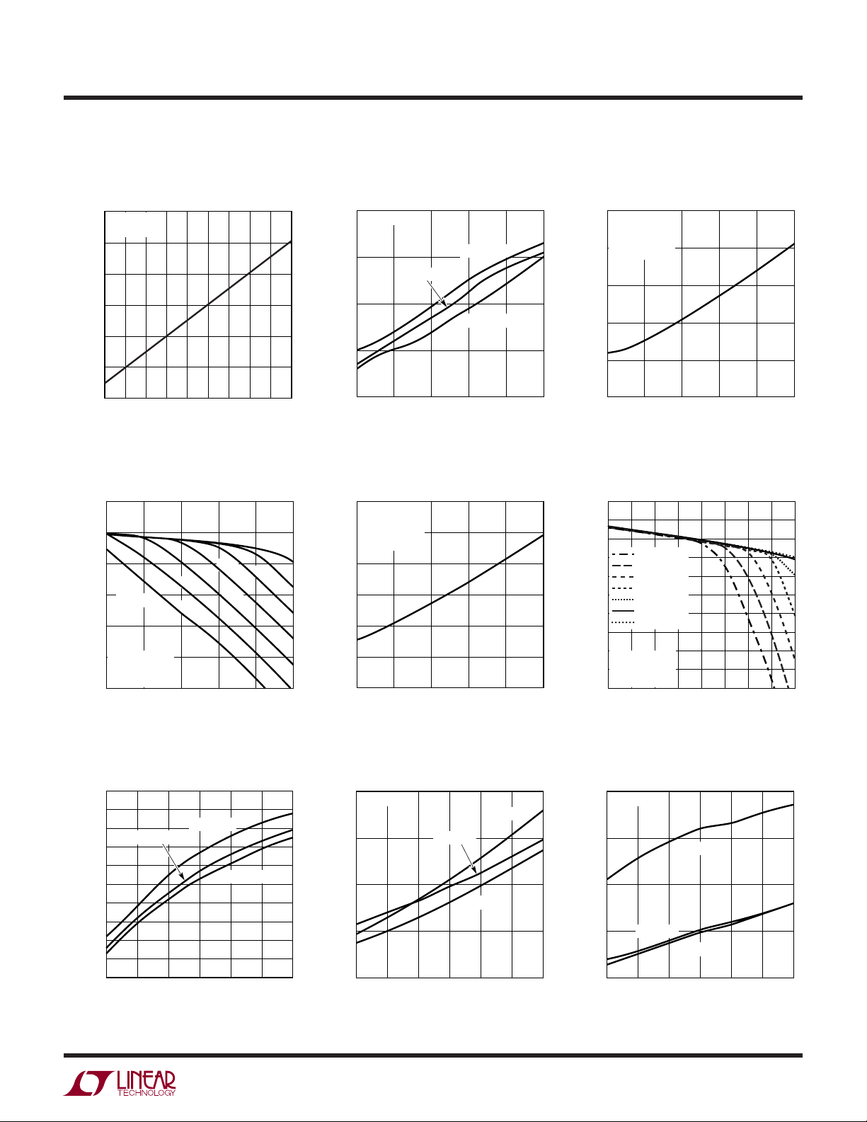
4-LED MAIN Display
Effi ciency vs Input Voltage
100
90
80
) (%)
70
IN
/P
60
LED
50
40
30
EFFICIENCY (P
20
4 LEDs AT 15mA/LED
AT 15mA = 3.2V)
(TYP V
F
10
= 25°C
T
A
0
3.2
3.0
3.6
3.4
3.8
V
(V)
BAT
4.0
4.44.2
3208 TA01b
3208fa
1
LTC3208
WW
W
U
ABSOLUTE AXI U RATI GS
(Note 1)
V
, DVCC, CPO to GND ................................– 0.3 to 6V
BAT
SDA, SCL, ENRGBS, CAMHL .....– 0.3V to (DV
(Note 2) ............................................................1.3A
I
CPO
I
MAIN1-4
, I
I
RED
I
CAM1-4
CPO, R
, I
GRN
, I
REF
AUX1-4
(Note 3) .......................................33mA
SUB1-2
, I
(Note 3) .......................................33mA
BLUE
(Note 3) ......................................120mA
Short-Circuit Duration .................... Indefi nite
Operating Temperature Range (Note 4) .. – 40°C to 85°C
Storage Temperature Range .................. – 65°C to 125°C
+ 0.3V)
CC
UUW
PACKAGE/ORDER I FOR ATIO
TOP VIEW
BAT1
CPO
C1P
V
C2P
ENRGBS
C1M
C2M
32 31 30 29 28 27 26 25
1CAM1
CAM2
2
CAM3
3
CAM4
4
AUX1
5
AUX2
6
AUX3
7
AUX4
8
9 10 11 12
CAMHL
32-LEAD (5mm × 5mm) QFN
EXPOSED PAD IS GND (PIN 33)
MUST BE SOLDERED TO PCB
T
JMAX
33
13 14 15 16
SDA
BAT3
R
V
UH PACKAGE
REF
SCL
= 125°C, θJA = 34°C/W
ORDER PART NUMBER UH PART MARKING
LTC3208EUH 3208
Order Options Tape and Reel: Add #TR
Lead Free: Add #PBF Lead Free Tape and Reel: Add #TRPBF
Lead Free Part Marking: http://www.linear.com/leadfree/
Consult LTC Marketing for parts specifi ed with wider operating temperature ranges.
GND
V
24
BAT2
RED
23
GRN
22
BLUE
21
SUB1
20
SUB2
19
MAIN4
18
MAIN3
17
VCC
D
MAIN1
MAIN2
●
The
ELECTRICAL CHARACTERISTICS
temperature range, otherwise specifi cations are at T
= 25°C. V
A
denotes the specifi cations which apply over the full operating
= 3.6V, DVCC = 3V, ENRGBS = Hi, R
BAT
= 24k, C2 = C3 = 2.2µF,
REF
C1 = C4 = 4.7µF, unless otherwise noted.
PARAMETERS CONDITIONS MIN TYP MAX UNITS
V
Operating Voltage
BAT
Operating Current I
I
VBAT
I
I
Operating Voltage
DV
CC
Operating Current DVCC = 1.8V, Serial Port Idle
DV
CC
UVLO Threshold 1.5 V
V
BAT
UVLO Threshold 1 V
DV
CC
Shutdown Current DVCC = 1.8V 3.2 µA
V
BAT
R
REF
VR
REF
RR
Reference Resistor Range
REF
= 0, 1x Mode, LEDs Disabled 280 µA
CPO
= 0, 1.5x Mode 4.7 mA
CPO
= 0, 2x Mode 7 mA
CPO
White LED Current (MAIN1-4, SUB1-2), 8-Bit Linear DACs
Full-Scale LED Current MAIN, SUB = 1V
Minimum (1LSB) LED Current MAIN, SUB = 1V 108 µA
LED Current Matching Any Two MAIN or SUB Outputs, 50% FS 1 %
LED Dropout Voltage I
= FS 180 mV
LED
●
2.9 4.5 V
●
1.5 5.5 V
●
1 µA
●
1.195 1.215 1.235 V
●
22 30 k
●
25.3 27.5 29.7 mA
3208fa
2
LTC3208
ELECTRICAL CHARACTERISTICS
The
temperature range, otherwise specifi cations are at T
= 25°C. V
A
C1 = C4 = 4.7µF, unless otherwise noted.
PARAMETERS CONDITIONS MIN TYP MAX UNITS
White LED Current (CAM1-4), 4-Bit Linear DAC
Full-Scale LED Current CAM = 1V
Minimum (1LSB) LED Current CAM = 1V 6.96 mA
LED Current Matching Any Two CAM Outputs, 50% FS 1 %
LED Dropout Voltage I
White LED Current (AUX1-4, AUX Outputs Assigned to AUX DAC), 4-Bit Linear DAC
Full-Scale LED Current AUX = 1V
Minimum (1LSB) LED Current AUX = 1V 1.73 mA
LED Current Matching Two AUX Outputs, 50% FS 1 %
LED Dropout Voltage I
Full-Scale AUX LED Current AUX Connected to CAM DAC, AUX = 1V 104.9 mA
Full-Scale AUX LED Current AUX Connected to SUB or MAIN DAC, AUX = 1V 28.1 mA
RGB LED Current (RED, GREEN, BLUE), 4-Bit Exponential DAC
DAC Code 0001 RED, GREEN, BLUE = 1V 0.24 mA
DAC Code 0010 RED, GREEN, BLUE = 1V 0.32 mA
DAC Code 0011 RED, GREEN, BLUE = 1V 0.46 mA
DAC Code 0100 RED, GREEN, BLUE = 1V 0.63 mA
DAC Code 0101 RED, GREEN, BLUE = 1V 0.89 mA
DAC Code 0110 RED, GREEN, BLUE = 1V 1.22 mA
DAC Code 0111 RED, GREEN, BLUE = 1V 1.74 mA
DAC Code 1000 RED, GREEN, BLUE = 1V 2.42 mA
DAC Code 1001 RED, GREEN, BLUE = 1V 3.47 mA
DAC Code 1010 RED, GREEN, BLUE = 1V 4.73 mA
DAC Code 1011 RED, GREEN, BLUE = 1V 6.7 mA
DAC Code 1100 RED, GREEN, BLUE = 1V 9.47 mA
DAC Code 1101 RED, GREEN, BLUE = 1V 13.56 mA
DAC Code 1110 RED, GREEN, BLUE = 1V 19.05 mA
DAC Code 1111 RED, GREEN, BLUE = 1V 27.06 mA
Charge Pump (CPO)
1x Mode Output Impedance 0.35
1.5x Mode Output Impedance V
2x Mode Output Impedance V
CPO Voltage Regulation 1.5x Mode, I
2x Mode, I
CLOCK Frequency
SDA, SCL, ENRGBS, CAMHL
V
, (Low Level Input Voltage)
IL
V
, (High Level Input Voltage)
IH
V
, Digital Output Low (SDA) I
OL
I
SDA, SCL, ENRGBS, CAMHL = DVCC
IH
I
SDA, SCL, ENRGBS, CAMHL = 0V
IL
Serial Port Timing (Notes 6, 7)
t
Clock Operating Frequency 400 kHz
SCL
t
Bus Free Time Between Stop and Start Condition 1.3 µs
BUF
t
Hold Time After (Repeated) Start Condition 0.6 µs
HD,STA
= FS 540 mV
LED
= FS 140 mV
LED
= 3V, V
BAT
BAT
PULLUP
= 3V, V
= 3mA
CPO
CPO
CPO
CPO
●
denotes the specifi cations which apply over the full operating
= 3.6V, DVCC = 3V, ENRGBS = Hi, R
BAT
●
92.5 102.5 112.5 mA
●
23 26 28.5 mA
= 4.2V (Note 5) 2
= 4.8V (Note 5) 2.2
= 2mA 4.53 V
= 2mA 5.02 V
●
0.6 0.9 1.2 MHz
●
●
●
●
–1 1 µA
●
–1 1 µA
= 24k, C2 = C3 = 2.2µF,
REF
0.3 • DVCC V
0.7 • DVCC V
0.18 0.4 V
3208fa
3
LTC3208
The
ELECTRICAL CHARACTERISTICS
temperature range, otherwise specifi cations are at T
= 25°C. V
A
●
denotes the specifi cations which apply over the full operating
= 3.6V, DVCC = 3V, ENRGBS = Hi, R
BAT
= 24k, C2 = C3 = 2.2µF,
REF
C1 = C4 = 4.7µF, unless otherwise noted.
PARAMETERS CONDITIONS MIN TYP MAX UNITS
Repeated Start Condition Setup Time 0.6 µs
t
SU,STA
t
Stop Condition Setup Time 0.6 µs
SU,STO
t
HD,DAT(OUT)
t
HD,DAT(IN)
t
SU,DAT
t
LOW
t
HIGH
t
Clock Data Fall Time 20 300 ns
f
t
Clock Data Rise Time 20 300 ns
r
t
SP
Note 1: Absolute Maximum Ratings are those values beyond which the
MTBF of a device may be impaired.
Note 2: Based on long-term current density limitations. Assumes an
operating duty cycle of ≤10% under absolute maximum conditions for
durations less than 10 seconds. Max charge pump current for continuous
operation is 500mA.
Note 3: Based on long-term current density limitations.
Data Hold Time 0 900 ns
Input Data Hold Time 0 ns
Data Setup Time 100 ns
Clock Low Period 1.3 µs
Clock High Period 0.6 µs
Spike Suppression Time 50 ns
Note 4: The LTC3208E is guaranteed to meet performance specifi cations
from 0°C to 70°C. Specifi cations over the –40°C to 85°C ambient
operating temperature range are assured by design, characterization and
correlation with statistical process controls.
Note 5: 1.5x mode output impedance is defi ned as (1.5V
2x mode output impedance is defi ned as (2V
Note 6: All values are referenced to V
IH
– V
BAT
and VIL levels.
CPO
)/I
BAT
OUT
– V
.
CPO
)/I
OUT
Note 7: Guaranteed by Design.
.
UW
TYPICAL PERFOR A CE CHARACTERISTICS
Mode Switch Dropout Times 1.5x Mode CPO Ripple 2x Mode CPO Ripple
V
CPO
1V/DIV
5V
TA = 25°C
= 3.6V
V
BAT
1x
1.5x
250µs/DIV
2x
20mV/DIV
AC COUPLED
3208 G01
TA = 25°C
= 3.6V
V
BAT
= 400mA
I
CPO
= 4.7µF
C
CPO
V
CPO
500ns/DIV
3208 G02
V
CPO
20mV/DIV
AC COUPLED
TA = 25°C
= 3.6V
V
BAT
= 400mA
I
CPO
= 4.7µF
C
CPO
500ns/DIV
3208 G03
4
3208fa
UW
TYPICAL PERFOR A CE CHARACTERISTICS
LED Pin Dropout Voltage
vs LED Pin Current
600
V
= 3.6V
BAT
= 25°C
T
A
500
400
300
200
100
LED PIN DROPOUT VOLTAGE (mV)
1x Mode Switch Resistance vs
Temperature
0.45
I
= 200mA
CPO
0.40
V
= 3.6V
BAT
0.35
0.30
SWITCH RESISTANCE (Ω)
V
V
BAT
BAT
= 3.3V
= 3.9V
LTC3208
1.5x Mode Charge Pump Open-Loop
Output Resistance vs Temperature
– V
2.5
2.3
2.1
1.9
SWITCH RESISTANCE (Ω)
1.7
(1.5V
BAT
V
= 3V
BAT
= 4.2V
V
CPO
C2 = C3 = 2.2µF
C4 = 4.7µF
CPO
)/I
CPO
0
10
20 40 50 10090
30 60 70 80
LED CURRENT (mA)
1.5x Mode CPO Voltage
vs Load Current
4.8
4.6
4.4
4.2
V
= 3V
BAT
4.0
CPO VOLTAGE (V)
C2 = C3 = 2.2µF
3.8
C4 = 4.7µF
= 25°C
T
A
3.6
100 200 300 400
LOAD CURRENT (mA)
Oscillator Frequency
vs Supply Voltage
940
930
920
910
900
890
880
FREQUENCY (kHz)
870
860
850
840
2.7
TA = 25°C
3.3 3.6 3.9
3.0
V
SUPPLY VOLTAGE (V)
BAT
3.2V
3.1V
TA = –40°C
3.4V
3.3V
TA = 85°C
3208 G04
3.6V
3.5V
3208 G07
4.2 4.5
3208 G10
0.25
–15 10 35 85
–40
TEMPERATURE (°C)
60
3208 G05
1.5
–15 10 35 85
–40
TEMPERATURE (°C)
60
3208 G06
2x Mode Charge Pump OpenLoop Output Resistance vs
– V
Temperature (2V
2.8
V
= 3V
BAT
= 4.8V
V
CPO
C2 = C3 = 2.2µF
2.6
C4 = 4.7µF
2.4
2.2
2.0
SWITCH RESISTANCE (Ω)
1.8
SHUTDOWN CURRENT (µA)
DV
1.6
0.4
0.3
0.2
0.1
CC
5000
–15 10 35 85
–40
Shutdown Current
DV
CC
vs DV
0
2.7
Voltage
CC
V
= 3.6V
BAT
3.0
BAT
TEMPERATURE (°C)
TA = 85°C
3.3 3.6 3.9
DVCC VOLTAGE (V)
CPO
TA = –40°C
TA = 25°C
)/I
CPO
60
3208 G08
4.2 4.5
3208 G11
2x Mode CPO Voltage
vs Load Current
5.2
5.1
5.0
4.9
4.8
4.7
4.6
CPO VOLTAGE (V)
4.5
4.4
4.3
4.2
8.5
7.5
6.5
5.5
4.5
3.5
SHUTDOWN CURRENT (µA)
BAT
V
2.5
1.5
V
= 3V
BAT
= 3.1V
V
BAT
= 3.2V
V
BAT
= 3.3V
V
BAT
= 3.4V
V
BAT
= 3.5V
V
BAT
= 3.6V
V
BAT
C2 = C3 = 2.2µF
C4 = 4.7µF
= 25°C
T
A
100 200 300 600 700
LOAD CURRENT (mA)
V
Shutdown Current
BAT
Voltage
vs V
BAT
D
= 3V
VCC
TA = 25°C
3.0
3.3 3.6 3.9
V
2.7
TA = 85°C
TA = –40°C
VOLTAGE (V)
BAT
800400 5000
3208 G09
4.2 4.5
3208 G12
3208fa
5
LTC3208
UW
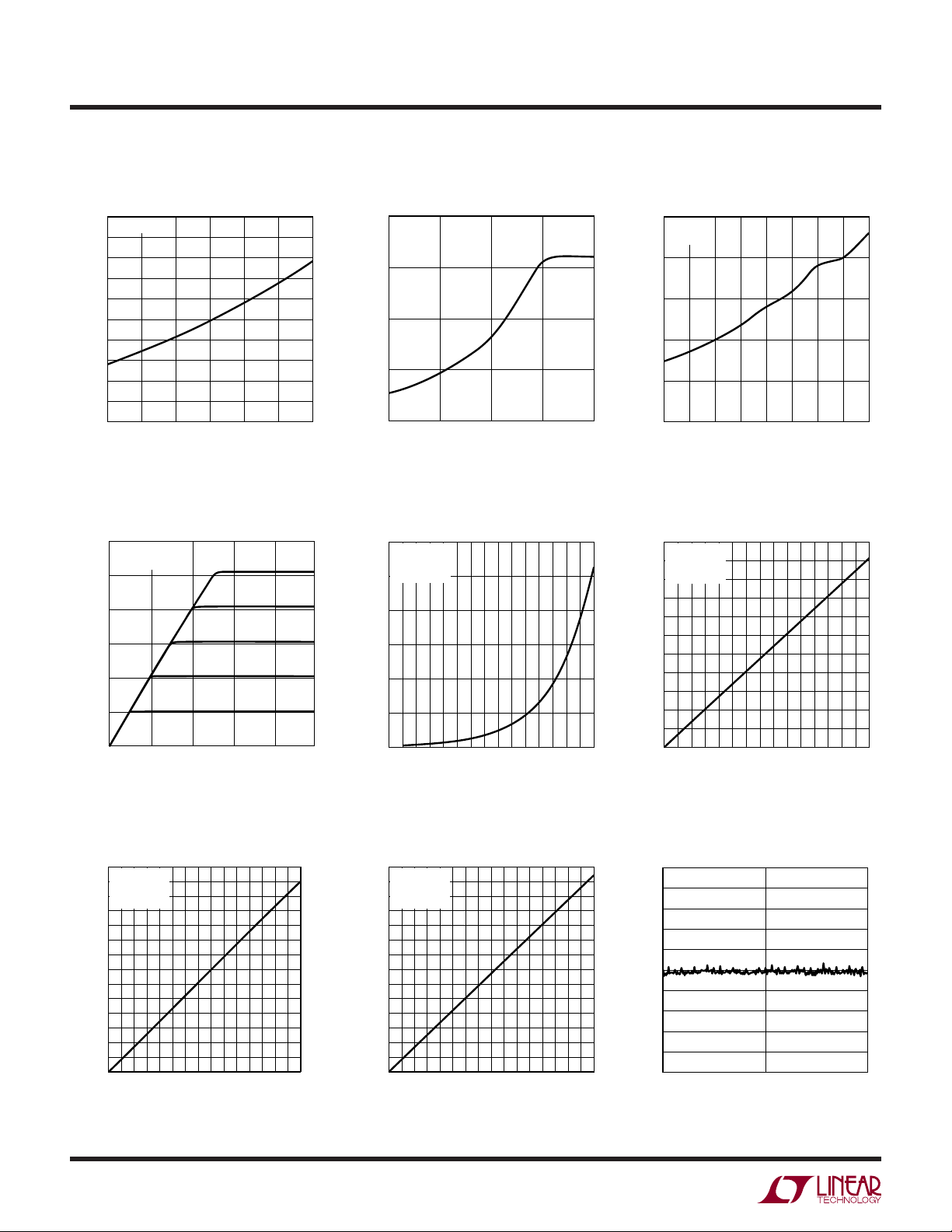
TYPICAL PERFOR A CE CHARACTERISTICS
1x Mode No Load V
Voltage
V
BAT
300
TA = 25°C
290
280
270
260
250
CURRENT (µA)
240
BAT
V
230
220
210
200
2.7
3.3 3.6 3.9
3.0
V
CAM Pin Current vs
CAM Pin Voltage
120
V
= 3.6V
BAT
= 25°C
T
A
100
80
60
40
CAM PIN CURRENT (mA)
20
0
0
0.2 0.4 0.6 0.8
CAM PIN VOLTAGE (V)
VOLTAGE (V)
BAT
Current vs
BAT
4.2 4.5
3208 G13
3208 G16
1.0
1.5x Mode Supply Current
vs I
(IV
CPO
40
VIN = 3.6V
= 25°C
T
A
30
20
SUPPLY CURRENT (mA)
10
0
0
– 1.5I
BAT
200 400 600
LOAD CURRENT (mA)
CPO
RGB LED Current vs Input Code
30
V
= 3.6V
BAT
= 25°C
T
A
= 24.3k
R
25
REF
20
15
10
RGB LED CURRENT (mA)
5
0
2468
HEX CODE
2x Mode Supply Current
)
800
3208 G14
vs I
(IV
CPO
25
VIN = 3.6V
= 25°C
T
A
20
15
10
SUPPLY CURRENT (mA)
5
0
0 200 400 600 800100 300 500 700
– 2I
BAT
CPO
LOAD CURRENT (mA)
)
3208 G15
CAM LED Current vs
Input Code
110
V
= 3.6V
BAT
100
= 25°C
T
A
= 24.3k
R
REF
90
80
70
60
50
40
30
CAM LED CURRENT (mA)
20
10
0
3208 G17
FEDCBA10 3579
2468
HEX CODE
FEDCBA10 3579
3208 G18
AUX LED Current vs Input Code
28
V
= 3.6V
BAT
26
= 25°C
T
A
24
= 24.3k
R
REF
22
20
18
16
14
12
10
8
AUX LED CURRENT (mA)
6
4
2
0
2468
HEX CODE
6
FEDCBA103579
3208 G21
Main/Sub LED Current vs
Input Code Main/Sub INL
28
V
= 3.6V
BAT
26
= 25°C
T
A
24
= 24.3k
R
REF
22
20
18
16
14
12
10
8
6
MAIN/SUB LED CURRENT (mA)
4
2
0
20 40 60 80
HEX CODE
FFF0E0D0C0B0A0100 30507090
3208 G19
1.0
0.8
0.6
0.4
0.2
0
–0.2
–0.4
MAIN/SUB INL (LSB)
–0.6
–0.8
–1.0
80
HEX CODE
FF1
3208 G20
3208fa

UUU
PI FU CTIO S
LTC3208
CAM1-4 (Pins 1, 2, 3, 4): Current Source Outputs for
the CAM Display White LEDs. The LEDs on the CAM
display can be set from 0mA to 102mA in 16 steps via
software control and internal 4-bit linear DAC. Two 4-bit
registers are available. One is used to program the high
camera current and the second the low camera current.
These registers can be selected via the serial port or the
CAMHL pin. Each output can be disabled by connecting
the output to CPO. Setting data in REGF to 0 disables all
CAM outputs. (See Applications Information.)
AUX1-4 (Pins 5, 6, 7, 8): Current Source Outputs for the
AUX Display White LEDs. When used as a separate display,
the LED current sources of the AUX display can be set
from 0mA to 26mA in 16 steps via software control and
internal 4-bit linear DAC. In addition, these outputs can
be connected individually as needed to the CAM, SUB or
MAIN displays and driven from each display’s associated
DAC. AUX 1, 2 and 3 can be disabled by connecting the
output to CPO. AUX 4 can be used as an open drain I
controlled logic output but cannot be disabled by connecting to CPO when confi gured as logic output. Setting
data in REGE and REGB2 to 0 disables all AUX outputs.
(See Applications Information.)
CAMHL (Pin 9): Logic Input. Selects CAM high register
when asserted High and CAM Low Register when low.
The high to low transition automatically resets the charge
pump mode to 1x.
SCL (Pin 10): I2C Clock Input. The logic level for SCL is
referenced to DVCC.
SDA (Pin 11): I2C Data Input for the Serial Port. Serial
data is shifted in one bit per clock to control the LTC3208.
The logic level is referenced to DV
CC
.
2
C
V
BAT3, 2, 1
Device. Three separate pins are used to isolate the charge
pump from the analog sections to reduce noise. All pins
must be connected together externally and bypassed with
a 4.7µF low ESR ceramic capacitor. The 4.7µF bypass
capacitor should be connected close to V
capacitor should be connected close to V
R
REF
Current for all Displays. The R
external resistor to ground sets the reference currents for
all display DACs and support circuits. Since this resistor
biases all circuits within the LTC3208, the value is limited
to a range of 22k to 30k.
DVCC (Pin 14): Supply Voltage for all Digital I/O Lines.
This pin sets the logic reference level of the LTC3208.
A UVLO circuit on the DVCC pin forces all registers to all
0s whenever DVCC is below the DVCC UVLO threshold.
Bypass to GND with a 0.1µF capacitor.
MAIN1-4 (Pins 15,16,17,18): Current Source Outputs
for the MAIN Display White LEDs. The LEDs on the MAIN
display can be set from 0µA to 27.5mA in 256 steps via
software control and internal 8-bit linear DAC. Each output
can be disabled externally by connecting the output to CPO.
Setting data in REGC to 0 disables all MAIN outputs.
SUB2, SUB1 (Pins 19, 20): Current Source Outputs for
the SUB Display White LEDs. The LEDs on the SUB display
can be set from 0µA to 27.5mA in 256 steps via software
control and an internal 8-bit linear DAC. Each output can
be disabled externally by connecting the output to CPO.
Setting the data in REGD to 0 disables all SUB outputs.
(Pins 12, 24, 30): Supply Voltage for the Entire
. A 0.1µF
BAT2
.
BAT3
(Pin 13): Controls the Maximum Amount of LED
voltage is 1.215V. An
REF
3208fa
7

LTC3208
UUU
PI FU CTIO S
BLUE, GRN, RED (Pins 21, 22, 23): Current Source
Outputs for the RGB Illuminator LEDs. The RGB currents
can be independently set via the serial port. Currents
up to 27mA can be programmed over 16 steps via the
three internal 4-bit exponential DACs. These outputs can
also be used as open drain I
When confi gured this way, these outputs cannot be externally disabled by connecting to CPO. Setting data to
0 in REGA1 disables RED, REGA2 disables GREEN and
REGB1 disables BLUE.
GND (Pins 25, 33): System Ground. Connect Pin 25 and
exposed pad Pin 33 directly to a low impedance ground
plane.
C2M, C1M, C2P, C1P (Pins 26, 27, 29, 31): Charge
Pump Flying Capacitor Pins. 2.2µF X7R or X5R ceramic
2
C controlled logic outputs.
capacitors should be connected from C1P to C1M and
C2P to C2M.
ENRGBS (Pin 28): Logic Input. This pin is normally high
and is used to enable or disable the RED, GREEN and
BLUE LEDs or the SUB LEDs. The selection between RGB
or SUB is made via an internal programmable bit. When
the pin is toggled from low (disable) to high (enable), the
LTC3208 illuminates either the RGB display with a color
combination that was previously programmed, or the SUB
display at its previously programmed current. The logic
level is referenced to DV
CPO (Pin 32): Output of the Charge Pump Used to Power
All LEDs. A 4.7µF X5R or X7R ceramic capacitor should
be connected to ground.
CC
.
8
3208fa

BLOCK DIAGRA
V
BAT1
30
V
BAT2
24
V
BAT3
12
R
13
REF
DV
14
CC
ENRGBS
28
9
CAMHL
SDA
11
SCL
10
W
900kHz
OSCILLATOR
–
+
+
–
1.215V
SLAVE REG
REGISTER
V
CONTROL
LOGIC
MASTER/
SHIFT
C1P C1M C2P C2M
31
CHARGE PUMP
27
3
29 26
MAIN CURRENT
SOURCES
SUB CURRENT
SOURCES
AUX CURRENT
SOURCES
CAM CURRENT
SOURCES
RGB CURRENT
SOURCES
ENABLE CP
LTC3208
25
GND
32
CPO
MAIN1
15
MAIN2
16
MAIN3
17
4
2
4
4
MAIN4
18
SUB2
19
SUB1
20
AUX1
5
AUX2
6
RED GRN BLUE CAM1 CAM2 CAM3 CAM4 AUX4 AUX3
U
OPERATIO
Power Management
The LTC3208 uses a switched capacitor charge pump to
boost CPO to as much as 2 times the input voltage up to
5V. The part starts up in 1x mode. In this mode, V
connected directly to CPO. This mode provides maximum
effi ciency and minimum noise. The LTC3208 will remain in
this mode until an LED current source drops out. Dropout
occurs when a current source voltage becomes too low
for the programmed current to be supplied. When dropout
is detected, the LTC3208 will switch into 1.5x mode. The
CPO voltage will then start to increase and will attempt to
reach 1.5x V
up to 4.5V. Any subsequent dropout will
BAT
cause the part to enter the 2X mode. The CPO voltage will
attempt to reach 2x V
up to 5V. The part will be reset to
BAT
BAT1,2
are
21212223 3 4 8 7
1x mode whenever a DAC data bit is updated via the I
3208 BD
2
C
port or on the falling edge of the CAMHL signal.
A two-phase nonoverlapping clock activates the charge
pump switches. In the 2x mode the fl ying capacitors are
charged on alternate clock phases from V
to minimize
BAT
input current ripple and CPO voltage ripple. In 1.5x mode
the fl ying capacitors are charged in series during the fi rst
clock phase and stacked in parallel on V
during the
BAT
second phase. This sequence of charging and discharging
the fl ying capacitors continues at a constant frequency of
900kHz.
The currents delivered by the LED current sources are
controlled by an associated DAC. Each DAC is programmed
2
via the I
C port. The full scale DAC currents are set by R
The value of R
is limited to the range of 22k to 30k.
REF
REF
3208fa
.
9

LTC3208
OPERATIO
U
Soft-Start
Initially, when the part is in shutdown, a weak switch connects V
to CPO. This allows V
BAT
to slowly charge
BAT1,2
the CPO output capacitor and prevent large charging
currents to occur.
The LTC3208 also employs a soft-start feature on its charge
pump to prevent excessive inrush current and supply voltage droop when switching into the step-up modes. The
current available to the CPO pin is increased linearly over
a typical period of 150µs. Soft start occurs at the start of
both 1.5x and 2x mode changes.
Charge Pump Strength
When the LTC3208 operates in either 1.5x mode or 2x mode,
the charge pump can be modeled as a Thevenin-equivalent
circuit to determine the amount of current available from
the effective input voltage and effective open-loop output
resistance, R
is dependent on a number of factors including the
R
OL
switching term, 1/(2f
(Figure 1).
OL
OSC
• C
), internal switch resistances
FLY
and the nonoverlap period of the switching circuit. However,
for a given R
directly proportional to the advantage voltage of 1.5V
- CPO for 1.5x mode and 2V
, the amount of current available will be
OL
-CPO for 2x mode. Consider
BAT
BAT
the example of driving white LEDs from a 3.1V supply. If
the LED forward voltage is 3.8V and the current sources
require 100mV, the advantage voltage for 1.5x mode is
3.1V • 1.5 – 3.8V – 0.1V or 750mV. Notice that if the input
voltage is raised to 3.2V, the advantage voltage jumps to
900mV-a 20% improvement in available strength.
For 2X mode, the available current is given by:
VV
I
OUT
2–
BAT CPO
=
R
OL
(2)
Notice that the advantage voltage in the 2x case is
3.1V • 2 – 3.8V – 0.1V = 2.3V. R
is higher in 2x mode, but a
OL
significant overall increase in available current is
achieved.
Typical values of R
as a function of temperature are
OL
shown in Figure 2 and Figure 3.
2.5
V
= 3V
BAT
= 4.2V
V
CPO
C2 = C3 = 2.2µF
2.3
C4 = 4.7µF
2.1
1.9
SWITCH RESISTANCE (Ω)
1.7
1.5
Figure 2. Typical 1.5x ROL vs Temperature
2.8
2.6
2.4
–15 10 35 85
–40
TEMPERATURE (°C)
V
= 3V
BAT
= 4.8V
V
CPO
C2 = C3 = 2.2µF
C4 = 4.7µF
60
3208 F02
From Figure 1, for 1.5x mode the available current is
given by:
VV
I
OUT
Figure 1. Charge Pump Thevenin–Equivalent Open-Loop Circuit
15.–
BAT CPO
=
R
OL
+
–
(1)
R
1.5V
BAT
OL
OR 2V
BAT
+
CPO
–
3208 F01
10
2.2
2.0
SWITCH RESISTANCE (Ω)
1.8
1.6
Figure 3. Typical 2x ROL vs Temperature
–15 10 35 85
–40
TEMPERATURE (°C)
60
3208 F03
3208fa

OPERATIO
LTC3208
U
Shutdown Current
Shutdown occurs when all the current source data bits
have been written to zero or when DV
UVLO threshold.
Although the LTC3208 is designed to have very low shutdown current, it will draw about 3µA from V
shutdown. Internal logic ensures that the LTC3208 is in
shutdown when DV
all of the logic signals that are referenced to DV
SDA, ENRGBS, CAMHL) will need to be at DV
(i.e., ground) to avoid violation of the absolute maximum
specifi cations on these pins.
Serial Port
The microcontroller compatible I
of the command and control inputs for the LTC3208. Data
on the SDA input is loaded on the rising edge of SCL. D7
is loaded fi rst and D0 last. There are seven data registers,
one address register and one sub-address register. Once
all address bits have been clocked into the address register acknowledgment occurs. The sub-address register
is then written followed by writing the data register. Each
data register has a sub-address. After the data register
has been written a load pulse is created after the stop bit.
The load pulse transfers all of the data held in the data
registers to the DAC registers. The stop bit can be delayed
until all of the data master registers have been written.
At this point the LED current will be changed to the new
settings. The serial port uses static logic registers so there
is no minimum speed at which it can be operated.
MAIN and SUB Current Sources
There are four MAIN current sources and two SUB current
sources. Each bank of current sources has an 8-bit linear
DAC for current control. The output current range is 0 to
27.5mA in 256 steps.
The current sources are disabled when a block receives
an all zero data word. The supply current for that block is
reduced to zero. In addition each individual LED output
can be connected to CPO to turn off that particular current
source output and reduce operating current of the disabled
output to typically 10µA.
is grounded. Note, however, that
CC
is below the DVCC
CC
when in
BAT
(SCL,
CC
or below
CC
2
C serial port provides all
Camera Current Sources
There are four CAM current sources. This bank of current
sources has a 4-bit linear DAC for current control. The
output current range is 0 to 102mA in 16 steps.
The current sources are disabled when the block receives
an all zero data word. The supply current for the block is
reduced to zero. In addition each individual LED output
can be connected to CPO to turn off that particular current
source output and reduce operating current of the disabled
output to typically 10µA.
RGB Illuminators
The RED, GREEN and BLUE LEDs can be individually set
from 0µA to 27mA in 16 steps via three 4-bit exponential
DACs.
The current sources are individually disabled when an
all-zero data word is received. The supply current for the
current source is reduced to zero. These outputs can also
be used as open drain logic control outputs. For this reason
they will not be disabled when connected to CPO.
Auxiliary Current Sources
There are four AUX current sources. This bank of current
sources has a 4-bit linear DAC for current control. The
output current range is 0mA to 26mA in 16 steps.
In addition, each current source can be independently
connected to the CAM, SUB or MAIN DAC outputs. The
selection is made through the I
will then match the corresponding selected current source
bank. In this case a range of 0mA to 27.5mA for SUB and
MAIN or 0mA to 102mA for CAM will be achieved.
The current sources are disabled when the block receives
an all-zero data word in both REGE and REGB2. The supply current for the block is reduced to zero. AUX 1, 2 and
3 LED outputs can be connected to CPO to turn off that
particular current source output and reduce operating current of the disabled output to typically 10µA. AUX 4 can
be used as an open drain logic output and for this reason
will not be disabled if connected to CPO.
2
C port. The output current
3208fa
11

LTC3208
OPERATIO
U
Disabling Current Source Outputs
Unused CAM, SUB and MAIN outputs can be disabled by
using two different methods depending on the application
requirement. If the entire group is to be disabled (ie MAIN),
then the data register for that group is written to zero. The
unused outputs can be open circuit. If one or more of the
group outputs is to be enabled then the unused outputs
must be connected to CPO to prevent a false dropout
signal from occurring.
AUX has a mixture of disable requirements. If AUX is not
used then the data register is written to zero and all outputs can be left open circuit. If one or more output is to
be enabled then AUX1, AUX2 and AUX3 can be disabled
by connecting the unused output to CPO. AUX 4 cannot
be disabled by connecting to CPO but can be left open
circuit if X
dropout detector from the AUX4 output but also removes
the dropout detectors from the RED, GRN and BLUE LED
outputs. To avoid disabling the RED, GRN and BLUE
dropout detectors, AUX4 should be one of the enabled
outputs whenever a mixture of enabled and disabled AUX
outputs are used.
RED, GRN and BLUE outputs are disabled by writing the
unused output register to zero. The unused output can
be left open circuit.
CAMHL
RGBDROP
is set high. This setting removes the
the microcontroller. ENRGBS can be software programmed
as an independent control for either the RGB display or
the SUB display. Options REGG bit G1 determines which
display ENRGBS controls. When bit G1 is 0, the ENRGBS
pin controls the RGB display. If it is set to 1, then ENRGBS
controls the SUB display.
2
To use the ENRGBS pin, the I
to the desired setting. For example, if the ENRGBS pin will
be used to control the SUB display, then a nonzero code
must reside in REGD and Command register REGG bit
G1 must be set to 1. Now when ENRGBS is high (DV
the SUB display will be on with the REGD setting. When
ENRGBS is low the SUB display will be off. If no other
displays are programmed to be on, the entire chip will
be in shutdown.
Likewise if ENRGBS will be used to enable the RGB display,
then a nonzero code must reside in one of the RED, GREEN
or BLUE registers REGA1, REGA2 or REGB1, and options
register REGG bit G1 is set to 0. Now when ENRGBS is high
), the RGB display will light with the programmed
(DV
CC
color. When ENRGBS is low, the RGB display will be off.
If no other displays are programmed to be on, the entire
chip will be in shutdown.
If options register REGG bit G1 is set to 1 (SUB display
control), then ENRGBS will have no effect on the RGB
display. Likewise, if bit G1 is set to 0 (RGB display control),
then ENRGBS will have no effect on the SUB display.
C port must fi rst be confi gured
),
CC
The CAMHL pin quickly selects the camera high register
for fl ash applications without reaccessing the I
When low, the CAM current range will be controlled by
the camera low 4-bit register. When CAMHL is asserted
high, the current range will be set by the camera high
4-bit register.
ENRGBS Pin
The ENRGBS pin can be used to enable or disable the
LTC3208 without re-accessing the I
useful to indicate an incoming phone call without waking
2
C port. This might be
2
C port.
12
If the ENRGBS pin is not used, it must be connected to
. It should not be grounded or left fl oating.
DV
CC
Thermal Protection
The LTC3208 has built-in overtemperature protection.
At internal die temperatures of around 150°C thermal
shutdown will occur. This will disable all of the current
sources and charge pump until the die has cooled by about
15°C. This thermal cycling will continue until the fault has
been corrected.
3208fa

OPERATIO
LTC3208
U
R
Current Set Resistor
REF
The current set resistor is connected between RREF and
ground. The value of this resistor should typically be near
24k since all of the DAC reference currents and support
circuit currents are related to this set current.
This input is protected against shorts to ground or low
value resistors <10k. When a fault is detected the reference
current amplifi er is current limited. In addition, the current
source outputs and charge pump are disabled.
Fullscale LED Current Equations
V
1 215
AUX fullscale LEDcurrent Amps
SUB MAIN fullscaleLED current Amps
/
CAM fullscaleLED current Amps
RGB fullscale LEDcurrent Amps
()
()
()
.
=
R
REF
()
1 215
.
=
R
1 215
.
=
R
REF
=
REF
518
•
.
1 215
R
RE
V
202
•55
V
533
•
FF
V
•543
Mode Switching
The LTC3208 will automatically switch from 1x mode
to 1.5x mode and subsequently to 2x mode whenever
a dropout condition is detected at an LED pin. Dropout
occurs when a current source voltage becomes too low
for the programmed current to be supplied. The dropout
delay is typically 400µs.
The mode will automatically switch back to 1x whenever
2
a data bit is updated via the I
C port or when the CAMHL
pin switches from high to low.
2
C Interface
I
The LTC3208 communicates with a host (master) using
2
the standard I
C 2-wire interface. The Timing Diagram
(Figure 5) shows the timing relationship of the signals on
the bus. The two bus lines, SDA and SCL, must be high
when the bus is not in use. External pull-up resistors or
current sources, such as the LTC1694 SMBus accelerator,
are required on these lines.
The LTC3208 is a receive-only (slave) device.
SDA
SCL
ADDRESS WR
00110110
00110 110
123
456789123456789123456789
SDA
t
LOW
SU, DAT
t
HIGH
t
r
SCL
t
HD, STA
START
CONDITION
t
SUB-ADDRESS
S7 S6 S5 S4 S3 S2 S1 S0
ACK
S7 S6 S5 S4 S3 S2 S1 S0
Figure 4. Bit Assignments
t
HD, DAT
t
f
REPEATED START
CONDITION
Figure 5. Timing Parameters
t
SU, STA
t
HD, STA
DATA BYTE
76543210
ACK
76543210
t
SU, STO
t
SP
STOP
CONDITION
t
BUF
3208 F05
START
CONDITION
STOPSTART
ACK
3208 FO4
3208fa
13

LTC3208
OPERATIO
U
Write Word Protocol Used By the LTC3208
1 7 1 1 8 1 8 1 1
S SLAVE ADDRESS WR A *SUB-ADDRESS A DATA BYTE A P**
S = Start Condition, Wr = Write Bit = 0, A = Acknowledge,
P = Stop Condition
*The sub-address uses only the fi rst 3 bits, D0, D1 and D2.
**Stop can be delayed until all of the data registers have been written.
REGA, RED LED and GREEN LED 4-Bit DAC Data, Register Sub-Address = 001
MSB REGA2 LSB MSB REGA1 LSB
A7 A6 A5 A4 A3 A2 A1 A0
GRN D3 GRN D2 GRN D1 GRN D0 RED D3
REGB, BLUE LED and AUXILIARY 4-Bit DAC Data, Register Sub-Address = 010
MSB REGB2 LSB MSB REGB1 LSB
B7 B6 B5 B4 B3 B2 B1 B0
AUX D3 AUX D2 AUX D1 AUX D0 BLUE D3 BLUE D2 BLUE D1 BLUE D0
Sub-Address Byte
MSB LSB
S7 S6 S5 S4 S3 S2 S1 S0 REGISTER
X X X X X 0 0 0 NONE
X X X X X 0 0 1 REGA
X X X X X 0 1 0 REGB
X X X X X 0 1 1 REGC
X X X X X 1 0 0 REGD
X X X X X 1 0 1 REGE
X X X X X 1 1 0 REGF
X X X X X 1 1 1 REGG
RED D2
RED D1
RED D0
REGC, MAIN LED 8-Bit DAC Data, Register Sub-Address = 011
MSB LSB
C7 C6 C5 C4 C3 C2 C1 C0
MAIN D7 MAIN D6 MAIN D5 MAIN D4 MAIN D3 MAIN D2 MAIN D1 MAIN D0
REGD, SUB LED 8-Bit DAC Data, Register Sub-Address = 100
MSB LSB
D7 D6 D5 D4 D3 D2 D1 D0
SUB D7 SUB D6 SUB D5 SUB D4 SUB D3
SUB D2
SUB D1
SUB D0
3208fa
14

OPERATIO
LTC3208
U
REGE, AUXILIARY LED 8-Bit MUX Data, Selects DAC for Each AUX Output, Register Sub-Address = 101
AUX4 AUX3 AUX2 AUX1
E7 E6 SELECT E5 E4 SELECT E3 E2 SELECT E1 E0 SELECT
0 0 AUX 0 0 AUX 0 0 AUX 0 0 AUX
0 1 MAIN 0 1 MAIN 0 1 MAIN 0 1 MAIN
1 0 SUB 1 0 SUB 1 0 SUB 1 0 SUB
1 1 CAM 1 1 CAM 1 1 CAM 1 1 CAM
REGF, CAMERA LED 4-Bit High and 4-Bit Low DAC Data, Register Sub-Address = 110
MSB HIGH BITS LSB MSB LOW BITS LSB
F7 F6 F5 F4 F3 F2 F1 F0
CAM D3 CAM D2 CAM D1 CAM D0 CAM D3
REGG, Options Byte, Sub-Address = 111
MSB LSB
G7 G6 G5 G4 G3 G2 G1 G0
Force2x Force1p5 D
D
TH2
TH1
X
RGBDROP SCAMHILO
CAM D2 CAM D1 CAM D0
S
ELRGBS
Not Used
S
(G1) 1 Selects SUB displays for control by the ENRGBS pin
ELRGBS
0 Selects RGB displays for control by the ENRGBS pin
S
0 Selects CAM low register, enables CAMHL pin
X
0 Enables RGB and AUX4 dropout signals
D
D
Force1p5 (G6) 1 Forces charge pump into 1.5x mode
0 Enables mode logic to control mode changes based on dropout signal
Force2x (G7) 1 Forces charge pump into 2x mode, overrides Force1p5 signal
0 Enables mode logic to control mode changes based on dropout signal
(G2) 1 Selects CAM high register, disables CAMHL pin
CAMHILO
RGBDROP
TH1
TH2
(G3) 1 Disables RGB and AUX4 dropout signals when outputs used as logic signals
(G4) 0 Test hook, must always be 0
(G5) 0 Test hook, must always be 0
3208fa
15

LTC3208
OPERATIO
U
Bus Speed
2
C port is designed to be operated at speeds of up
The I
to 400kHz. It has built-in timing delays to ensure correct
operation when addressed from an I
device. It also contains input fi lters designed to suppress
glitches should the bus become corrupted.
START and STOP Conditions
A bus-master signals the beginning of a communication
to a slave device by transmitting a START condition.
A START condition is generated by transitioning SDA
from high to low while SCL is high. When the master has
fi nished communicating with the slave, it issues a STOP
condition by transitioning SDA from low to high while
SCL is high. The bus is then free for communication with
another I
Byte Format
Each byte sent to the LTC3208 must be 8 bits long followed by an extra clock cycle for the Acknowledge bit to
be returned by the LTC3208. The data should be sent to
the LTC3208 most signifi cant bit (MSB) fi rst.
Acknowledge
The Acknowledge signal is used for handshaking between
the master and the slave. An Acknowledge (active LOW)
generated by the slave (LTC3208) lets the master know
that the latest byte of information was received. The
Acknowledge related clock pulse is generated by the
master. The master releases the SDA line (HIGH) during
the Acknowledge clock cycle. The slave-receiver must pull
down the SDA line during the Acknowledge clock pulse
so that it remains a stable LOW during the HIGH period
of this clock pulse.
Slave Address
The LTC3208 responds to only one 7-bit address which
has been factory programmed to 0011011. The eighth bit
of the address byte (R/W) must be 0 for the LTC3208 to
recognize the address since it is a write only device. This
effectively forces the address to be 8 bits long where the
least signifi cant bit of the address is 0. If the correct seven
bit address is given but the R/W bit is 1, the LTC3208 will
not respond.
2
C device.
2
C compliant master
Bus Write Operation
The master initiates communication with the LTC3208
with a START condition and a 7-bit address followed by
the Write Bit R/W = 0. If the address matches that of the
LTC3208, the LTC3208 returns an Acknowledge. The master should then deliver the most signifi cant sub-address
byte for the data register to be written. Again the LTC3208
acknowledges and then the data is delivered starting with
the most signifi cant bit. This cycle is repeated until all of the
required data registers have been written. Any number of
data latches can be written. Each data byte is transferred to
an internal holding latch upon the return of an Acknowledge.
After all data bytes have been transferred to the LTC3208,
the master may terminate the communication with a STOP
condition. Alternatively, a REPEAT-START condition can be
initiated by the master and another chip on the I
be addressed. This cycle can continue indefi nitely and the
LTC3208 will remember the last input of valid data that it
received. Once all chips on the bus have been addressed
and sent valid data, a global STOP condition can be sent
and the LTC3208 will update all registers with the data
that it had received.
In certain circumstances the data on the I
become corrupted. In these cases the LTC3208 responds
appropriately by preserving only the last set of complete
data that it has received. For example, assume the LTC3208
has been successfully addressed and is receiving data
when a STOP condition mistakenly occurs. The LTC3208
will ignore this stop condition and will not respond until a
new START condition, correct address, sub-address and
new set of data and STOP condition are transmitted.
Likewise, if the LTC3208 was previously addressed and
sent valid data but not updated with a STOP, it will respond
to any STOP that appears on the bus with only one exception, independent of the number of REPEAT-START’s
that have occurred. If a REPEAT-START is given and the
LTC3208 successfully acknowledges its address, it will
not respond to a STOP until all bytes of the new data have
been received and acknowledged.
Shared data registers will have all 8 bits rewritten since a
common acknowledge signal writes these registers. The
shared registers include REGA, REGB and REGF.
2
C bus can
2
C bus may
3208fa
16

LTC3208
U
WUU
APPLICATIO S I FOR ATIO
V
, CPO Capacitor Selection
BAT
The value and type of capacitors used with the LTC3208
determine several important parameters such as regulator
control loop stability, output ripple, charge pump strength
and minimum start-up time.
To reduce noise and ripple, it is recommended that low
equivalent series resistance (ESR) ceramic capacitors are
used for both CV
BAT
and C
capacitors are not recommended due to high ESR.
The value of C
directly controls the amount of output
CPO
ripple for a given load current. Increasing the size of C
will reduce output ripple at the expense of higher start-up
current. The peak-to-peak output ripple of the 1.5X mode
is approximately given by the expression
V
RIPPLE P P
−
Where f
is the LTC3208 oscillator frequency or typically
OSC
900kHz and C
CPO
I
OUT
=
fC
3•
OSC CPO
is the output storage capacitor.
The output ripple in 2x mode is very small due to the fact
that load current is supplied on both cycles of the clock.
Both value and type of output capacitor can signifi cantly
affect the stability of the LTC3208. As shown in the block
diagram, the LTC3208 uses a control loop to adjust the
strength of the charge pump to match the required output
current. The error signal of the loop is stored directly on the
output capacitor. The output capacitor also serves as the
dominant pole for the control loop. To prevent ringing or
instability, it is important for the output capacitor to maintain
at least 2.2µF of capacitance over all conditions.
. Tantalum and aluminum
CPO
(3)
CPO
value of CV
the input pin (V
controls the amount of ripple present at
BAT
). The LTC3208 input current will be
BAT
relatively constant while the charge pump is either in the
input charging phase or the output charging phase but will
drop to zero during the clock nonoverlap times. Since the
nonoverlap time is small (~25ns), these missing “notches”
will result in only a small perturbation on the input power
supply line. Note that a higher ESR capacitor such as tantalum will have higher input noise due to the higher ESR.
Therefore, ceramic capacitors are recommended for low
ESR. Input noise can be further reduced by powering the
LTC3208 through a very small series inductor as shown
in Figure 6. A 10nH inductor will reject the fast current
notches, thereby presenting a nearly constant current load
to the input power supply. For economy, the 10nH inductor
can be fabricated on the PC board with about 1cm (0.4”)
of PC board trace.
V
BAT
LTC3208
GND
3208 F06
Figure 6. 10nH Inductor Used for Input Noise Reduction
(Approximately 1cm of Board Trace)
Flying Capacitor Selection
Warning: Polarized capacitors such as tantalum or
aluminum should never be used for the fl ying capacitors since their voltage can reverse upon start-up of the
LTC3208. Ceramic capacitors should always be used for
the fl ying capacitors.
In addition, excessive output capacitor ESR will tend to
degrade the loop stability. The closed loop output resistance is about 80m . For a 100mA load current change,
the error signal will change by about 8mV. If the output
capacitor has 80m or more of ESR, the closed loop frequency response will cease to roll off in a simple one-pole
fashion and poor load transient response or instability may
occur. Multilayer ceramic chip capacitors typically have
exceptional ESR performance. MLCCs combined with a
tight board layout will result in very good stability. As the
value of C
controls the amount of output ripple, the
CPO
The fl ying capacitors control the strength of the charge
pump. In order to achieve the rated output current it is
necessary to have 2.2µF of capacitance for each of the
fl ying capacitors. Capacitors of different materials lose
their capacitance with higher temperature and voltage at
different rates. For example, a ceramic capacitor made of
X7R material will retain most of its capacitance from – 40°C
to 85°C, whereas a Z5U or Y5V style capacitor will lose
considerable capacitance over that range. Z5U and Y5V
capacitors may also have a very poor voltage coeffi cient
causing them to lose 60% or more of their capacitance when
3208fa
17

LTC3208
U
WUU
APPLICATIO S I FOR ATIO
the rated voltage is applied. Therefore, when comparing
different capacitors, it is often more appropriate to compare
the amount of achievable capacitance for a given case size
rather than comparing the specifi ed capacitance value. For
example, overrated voltage and temperature conditions, a
1µF, 10V, Y5V ceramic capacitor in a 0603 case may not
provide any more capacitance than a 0.22µF, 10V, X7R
available in the same case. The capacitor manufacturer’s
data sheet should be consulted to determine what value
of capacitor is needed to ensure minimum capacitances
at all temperatures and voltages.
Table 1 shows a list of ceramic capacitor manufacturers
and how to contact them:
Table 1. Recommended Capacitor Vendors
AVX www.avxcorp.com
Kemet www.kemet.com
Murata www.murata.com
Taiyo Yuden www.t-yuden.com
Vishay www.vishay.com
Layout Considerations and Noise
Due to its high switching frequency and the transient
currents produced by the LTC3208, careful board layout
is necessary. A true ground plane and short connections
to all capacitors will improve performance and ensure
proper regulation under all conditions.
The following guidelines should be followed when designing a PCB layout for the LTC3208.
• The exposed pad should be soldered to a large copper
plane that is connected to a solid, low impedance ground
plane using plated, through-hole vias for proper heat
sinking and noise protection.
• Input and output capacitors (C1 and C4) must be placed
close to the part.
• The fl ying capacitors (C2 and C3) must be placed close
to the part. The traces running from the pins to the
capacitor pads should be as wide as possible.
• V
, CPO traces must be made wide to minimize
BAT
inductance and handle the high currents.
• LED pads must be large and connected to other layers
of metal to ensure proper heat sinking.
GND PLANE
LAYER
GND
V
BAT
LAYER
CPO
C4
PLANE
GND
1
CONNECT TO
GND PLANE LAYER
C2
V
BAT
ALL VIAS LABELED GND
ARE CONNECTED TO
GND PLANE LAYER
C3
ALL VIAS LABELED V
ARE CONNECTED TO
PLANE LAYER
V
BAT
GND
C1
V
BAT
BAT
The fl ying capacitor pins C1P, C2P, C1M and C2M will have
very high edge rate waveforms. The large dv/dt on these
pins can couple energy capacitively to adjacent PCB runs.
Magnetic fi elds can also be generated if the fl ying capacitors
are not close to the LTC3208 (i.e., the loop area is large).
To decouple capacitive energy transfer, a Faraday shield
may be used. This is a grounded PCB trace between the
sensitive node and the LTC3208 pins. For a high quality
AC ground, it should be returned to a solid ground plane
that extends all the way to the LTC3208.
18
GND
V
BAT
C5
GND GND
R1
C6
R
REF
DV
Figure 7. PC Board Layout Example
V
GND
CC
BAT
LAYER
PLANE
GND PLANE
LAYER
3208 F07
3208fa

LTC3208
U
WUU
APPLICATIO S I FOR ATIO
Power Effi ciency
To calculate the power effi ciency (η) of a white LED
driver chip, the LED power should be compared to the
input power. The difference between these two numbers
represents lost power whether it is in the charge pump
or the current sources. Stated mathematically, the power
effi ciency is given by:
The effi ciency of the LTC3208 depends upon the mode in
which it is operating. Recall that the LTC3208 operates
as a pass switch, connecting V
is detected at the I
timum effi ciency available for a given input voltage and
LED forward voltage. When it is operating as a switch, the
effi ciency is approximated by:
since the input current will be very close to the sum of
the LED currents.
At moderate to high output power, the quiescent current
of the LTC3208 is negligible and the expression above is
valid.
Once dropout is detected at any LED pin, the LTC3208
switches the charge pump to 1.5x mode.
P
LED
η=
P
IN
(4)
pin. This feature provides the op-
LED
P
LED
η= = =
P
IN
•
VI
LED LED
•
VIVV
BAT BAT
to CPO, until dropout
BAT
LED
BAT
(5)
In 1.5x boost mode, the effi ciency is similar to that of a
linear regulator with an effective input voltage of 1.5 times
the actual input voltage. This is because the input current
for a 1.5x charge pump is approximately 1.5 times the
load current. In an ideal 1.5x charge pump, the power
effi ciency would be given by:
η
IDEAL
P
LED
== =
P
IN
VI
•
LED LED
VIVV
•.• .•15 15
BAT LED
LED
BAT
Similarly, in 2x boost mode, the effi ciency is similar to
that of a linear regulator with an effective input voltage
of 2 times the actual input voltage. In an ideal 2x charge
pump, the power effi ciency would be given by:
η
IDEAL
P
LED
== =
P
IN
VI
•
LED LED
VIVV
•• •22
BAT LED
LED
BAT
Thermal Management
For higher input voltages and maximum output current,
there can be substantial power dissipation in the LTC3208.
If the junction temperature increases above approximately
150°C, the thermal shutdown circuitry will automatically
deactivate the output current sources and charge pump.
To reduce maximum junction temperature, a good thermal
connection to the PC board is recommended. Connecting
the Exposed Pad to a ground plane and maintaining a solid
ground plane under the device will reduce the thermal
resistance of the package and PC board considerably.
3208fa
19

LTC3208
U
TYPICAL APPLICATIO S
6-LED MAIN, RGB Plus Low/High Current 8-LED Camera Light
C2
2.2µF
C3
2.2µF
V
D
ENABLE DISABLE
V
BAT
C1
4.7µF
0.1µF
D
VCC
0.1µF
ENABLE DISABLE
LOW HI
BAT
0.1µF
VCC
I2C
C1
4.7µF
I2C
LOW HI
C2
2.2µF
C1P C1M C2P C2M
V
BAT1
V
BAT2
V
BAT3
SCL/SDA
DV
CC
ENRGBS
CAMHL
R
REF
24.3k
1%
C1P C1M C2P C2M
V
BAT1
V
BAT2
V
BAT3
SCL/SDA
DV
0.1µF
ENRGBS
CAMHL
R
REF
24.3k
1%
CC
LTC3208
CPO
MAIN1-4
SUB1-2
CAM1-4
AUX1-4
RGB
GND
C4
4.7µF
4
2
4
4
3
MAIN CAMERA RGB
MAIN and SUB Backlight, Keypad Backlight, Camera Light and Camera Indicator
C3
2.2µF
CAMERA
INDICATOR
LTC3208
CPO
MAIN1-4
SUB1-2
CAM1-2
CAM3-4
RED
AUX1
AUX2
AUX3
AUX4
GRN
BLUE
GND
MAIN
C4
4.7µF
4
2
2
2
NC
NC
GRN AND BLUE DATA REGISTERS
SET TO ALL 0s
3208 TA02
KEYPADSUB CAMERA
3208 TA03
20
3208fa

U
TYPICAL APPLICATIO S
6-LED MAIN, 4-LED Camera Light, 7-LED Fun Lights
C2
2.2µF
C3
2.2µF
LTC3208
V
BAT
C1
4.7µF
0.1µF
I2C
DV
CC
0.1µF
ENABLE DISABLE
LOW HI
C1P C1M C2P C2M
V
BAT1
LTC3208
V
BAT2
V
BAT3
SCL/SDA
DV
CC
ENRGBS
CAMHL
R
REF
24.3k
1%
CPO
MAIN1-4
SUB1-2
CAM1-4
AUX1-4
RGB
GND
C4
4.7µF
4
2
4
4
3
MAIN CAMERA FUN LIGHTS
6-LED MAIN, RGB Plus Low/High Current 8-LED Camera Light with Tone Generator
C2
2.2µF
C3
2.2µF
3208 TA04
V
BAT
C1
4.7µF
0.1µF
I2C
DV
CC
0.1µF
ENABLE DISABLE
LOW HI
C1P C1M C2P C2M
V
BAT1
LTC3208
V
BAT2
V
BAT3
SCL/SDA
DV
CC
ENRGBS
CAMHL
R
REF
24.3k
1%
CPO
MAIN1-4
SUB1-2
CAM1-4
AUX1-4
RGB
GND
MAIN CAMERA RGB
C4
4.7µF
4
2
4
4
3
TONE CONTROL
3208 TA05
3208fa
21

LTC3208
U
TYPICAL APPLICATIO S
6-LED MAIN, 4-LED Camera Light, 4-LED Fun Lights with Vibrator Motor
C2
2.2µF
C3
2.2µF
V
BAT
C1
4.7µF
0.1µF
DV
CC
0.1µF
ENABLE DISABLE
LOW HI
I2C
C1P C1M C2P C2M
V
BAT1
LTC3208
V
BAT2
V
BAT3
SCL/SDA
DV
CC
ENRGBS
CAMHL
R
REF
24.3k
1%
MAIN CAMERA FUN LIGHTS
CPO
MAIN1-4
SUB1-2
CAM1-4
AUX1-4
RGB
GND
C4
4.7µF
4
2
4
4
3
10-LED MAIN with RED Camera Indicator, CAM Displays Disabled
C2
2.2µF
C3
2.2µF
BATT
VIBRATOR
MOTOR
3208 TA06
22
V
BAT
C1
4.7µF
0.1µF
I2C
DV
CC
0.1µF
ENABLE DISABLE
LOW HI
C1P C1M C2P C2M
V
BAT1
LTC3208
V
BAT2
V
BAT3
SCL/SDA
DV
CC
ENRGBS
CAMHL
R
REF
24.3k
1%
CPO
MAIN1-4
SUB1-2
AUX1-4
CAM1-4
RED
GRN
BLUE
GND
MAIN
C4
4.7µF
4
2
4
4
NC
NC
NC
GRN, BLUE AND CAM DATA REGISTERS
SET TO ALL 0s
CAM DISABLED
CAMERA
INDICATOR
3208 TA07
3208fa

PACKAGE DESCRIPTIO
5.50 ±0.05
4.10 ±0.05
3.45 ±0.05
(4 SIDES)
RECOMMENDED SOLDER PAD LAYOUT
5.00 ± 0.10
(4 SIDES)
PIN 1
TOP MARK
(NOTE 6)
U
UH Package
32-Lead Plastic QFN (5mm × 5mm)
(Reference LTC DWG # 05-08-1693)
0.70 ±0.05
PACKAGE OUTLINE
0.25 ± 0.05
0.50 BSC
0.75 ± 0.05
0.00 – 0.05
BOTTOM VIEW—EXPOSED PAD
R = 0.115
TYP
31
LTC3208
PIN 1 NOTCH R = 0.30 TYP
OR 0.35 × 45° CHAMFER
32
0.40 ± 0.10
1
2
3.45 ± 0.10
(4-SIDES)
0.200 REF
NOTE:
1. DRAWING PROPOSED TO BE A JEDEC PACKAGE OUTLINE
M0-220 VARIATION WHHD-(X) (TO BE APPROVED)
2. DRAWING NOT TO SCALE
3. ALL DIMENSIONS ARE IN MILLIMETERS
4. DIMENSIONS OF EXPOSED PAD ON BOTTOM OF PACKAGE DO NOT INCLUDE
MOLD FLASH. MOLD FLASH, IF PRESENT, SHALL NOT EXCEED 0.20mm ON ANY SIDE
5. EXPOSED PAD SHALL BE SOLDER PLATED
6. SHADED AREA IS ONLY A REFERENCE FOR PIN 1 LOCATION
ON THE TOP AND BOTTOM OF PACKAGE
0.25 ± 0.05
(UH32) QFN 1004
0.50 BSC
Information furnished by Linear Technology Corporation is believed to be accurate and reliable.
However, no responsibility is assumed for its use. Linear Technology Corporation makes no representation that the interconnection of its circuits as described herein will not infringe on existing patent rights.
3208fa
23

LTC3208
TYPICAL APPLICATIO
U
6-LED MAIN, 800mA Camera LED, Plus RGB Driver
C3
C2
2.2µF
2.2µF
V
BAT
C1
4.7µF
C5
0.1µF
DV
CC
C6
0.1µF
ENABLE DISABLE
LOW HI
I2C
24.3k
C1P C1M C2P C2M
V
BAT1
LTC3208
V
BAT2
V
BAT3
SCL/SDA
DV
ENRGBS
CAMHL
R
1%
MAIN1-4
CC
REF
CPO
SUB1-2
CAM1-4
AUX1-4
RGB
GND
MAIN
C4
4.7µF
4
2
4
4
3
D1 = Lumiled LXCL-PWF1
CAMERA
D1
RELATED PARTS
PART NUMBER DESCRIPTION COMMENTS
LT®1618 Constant Current, Constant Voltage, 1.4MHz Up to 16 White LEDs, VIN: 1.6V to 18V, V
High Effi ciency Boost Regulator I
LTC1911-1.5 250mA (I
), 1.5MHz High Effi ciency 75% Effi ciency, VIN: 2.7V to 5.5V, V
OUT
Step-Down Charge Pump I
LT1932 Constant Current, 1.2MHz High Effi ciency White Up to 8 White LEDs, VIN: 1V to 10V, V
LED Boost Regulator ThinSOT
LT1937 Constant Current, 1.2MHz High Effi ciency White Up to 4 White LEDs, VIN: 2.5V to 10V, V
LED Boost Regulator I
LTC3200-5 Low Noise, 2MHz Regulated Charge Pump Up to 6 White LEDs, VIN: 2.7V to 4.5V, V
White LED Driver ThinSOT Package
LTC3201 Low Noise, 1.7MHz Regulated Charge Pump Up to 6 White LEDs, V
White LED Driver 10-Lead MS
LTC3202 Low Noise, 1.5MHz Regulated Charge Pump Up to 8 White LEDs, V
White LED Driver 10-Lead MS Package
LTC3205 Multidisplay LED Controller 92% Effi ciency, V
4mm × 4mm QFN Package
LTC3206 I
2
C Multidisplay LED Controller 92% Effi ciency, 400mA Continuous Output Current. Up to 11 White LEDs in
4mm x 4mm QFN Package
LTC3216 1A High Current, Low Noise, White LED Driver 93% Effi ciency, V
Low/High Current Programming
LTC3251 500mA (I
), 1MHz to 1.6MHz Spread Spectrum 85% Effi ciency, VIN: 3.1V to 5.5V, V
OUT
Step-Down Charge Pump I
LTC3405/LTC3405A 300mA (I
), 1.5MHz Synchronous Step-Down 95% Effi ciency, VIN: 2.7V to 6V, V
OUT
DC/DC Converter ThinSOT Package
LTC3406/LTC3406B 600mA (I
), 1.5MHz Synchronous Step-Down 95% Effi ciency, VIN: 2.5V to 5.5V, V
OUT
DC/DC Converter ThinSOT Package
LTC3440 600mA (I
), 2MHz Synchronous Buck-Boost 95% Effi ciency, VIN: 2.5V to 5.5V, V
OUT
DC/DC Converter 10-Lead MS Package
LT3465/LT3465A 1.2MHz/2.7MHz with Internal Schottky Up to 6 White LEDs, V
I
ThinSOT is a trademark of Linear Technology Corporation.
Linear Technology Corporation
24
1630 McCarthy Blvd., Milpitas, CA 95035-7417
(408) 432-1900 ● FAX: (408) 434-0507
●
www.linear.com
≤1µA, 10-Lead MS Package
SD
≤10µA, MS8 Package
SD
TM
Package
≤1µA, ThinSOT, SC70 Packages
SD
: 2.7V to 4.5V, V
IN
: 2.7V to 4.5V, V
IN
: 2.8V to 4.5V, IQ = 50µA, ISD ≤ 1µA,
IN
: 2.9V to 4.4V, 1x/1.5x/2x Boost Modes, Independent
IN
≤1µA, 10-Lead MS Package
SD
: 12.7V to 16V, V
<1µA, ThinSOT Package
SD
IN
OUT(MIN)
OUT(MAX)
OUT
OUT(MIN)
OUT(MIN)
OUT(MIN)
INDICATOR
BGR
3208 TA08
= 34V, IQ = 1.8mA,
OUT(MAX)
= 1.5V/1.8V, IQ = 180µA,
= 34V, IQ = 1.2mA, IS ≤1µA,
= 34V, IQ = 1.9mA,
OUT(MAX)
= 5V, IQ = 8mA, ISD ≤1µA,
OUT(MAX)
= 5V, IQ = 6.5mA, ISD ≤1µA,
OUT(MAX)
= 5V, IQ = 5mA, ISD ≤1µA,
OUT(MAX)
: 0.9V to 1.6V, IQ = 9µA,
= 0.8V, IQ = 20µA, ISD ≤1µA,
= 0.6V, IQ = 20µA, ISD ≤1µA,
= 2.5V, IQ = 25µA, ISD ≤1µA,
= 34V, IQ = 1.9mA,
OUT(MAX)
LT 0106 REV A • PRINTED IN USA
© LINEAR TECHNOLOGY CORPORATION 2005
3208fa
 Loading...