

FEATURES
■
Step-Up/Direct-Connect Fractional Charge Pump
Provides Up to 92% Efficiency
■
Up to 400mA Continuous Output Current
■
Independent Current and Dimming Control for
1-6 LED MAIN, 1-4 LED SUB and RGB LED Displays
■
LED Currents Programmable Using 2-Wire I2C™
Serial Interface
■
1% LED Current Matching
■
Low Noise Constant Frequency Operation*
■
Minimal Component Count
■
Automatic Soft-Start Limits Inrush Current
■
16 Exponentially Spaced Dimming States Provides
128:1 Brightness Range for MAIN and SUB Displays
■
Up to 4096 Color Combinations for RGB Display
■
Low Operating Current: I
■
Tiny, Low Profile 24-Lead (4mm × 4mm × 0.75mm)
= 180µA
VIN
QFN Package
U
APPLICATIO S
■
Cellular Phones
■
Wireless PDAs
■
Multidisplay Handheld Devices
, LTC and LT are registered trademarks of Linear Technology Corporation.
I2C is a trademark of Philips Electronics N.V.
* U.S. Patent 6,411,531
LTC3206
I2C Multidisplay
LED Controller
U
DESCRIPTIO
The LTC®3206 is a highly integrated multidisplay LED controller. The part contains a high efficiency, low noise fractional step-up/direct-connect charge pump to provide
power for both main and sub white LED displays plus an
RGB color LED display. The LTC3206 requires only four
small ceramic capacitors plus two resistors to form a
complete 3-display LED power supply and current
controller.
Maximum currents for the main/sub displays and RGB
display are set independently. Current for each LED is
controlled with an internal current source. Dimming and
ON/OFF control for all displays is achieved via a 2-wire
serial interface. Two auxiliary LED pins can be individually
assigned to either the MAIN or SUB displays. 16 individual
dimming states exist for both the MAIN and SUB displays.
Each of the RED, GREEN and BLUE LEDs have 16 dimming
states as well, resulting in up to 4096 color combinations.
The LTC3206 charge pump optimizes efficiency based on
V
and LED forward voltage conditions. The part powers
IN
up in direct-connect mode and automatically switches to
1.5x step-up mode once any enabled LED current source
begins to enter dropout. Internal circuitry prevents inrush
current and excess input noise during start-up and mode
switching. The LTC3206 is available in a 24-lead (4mm ×
4mm) QFN package.
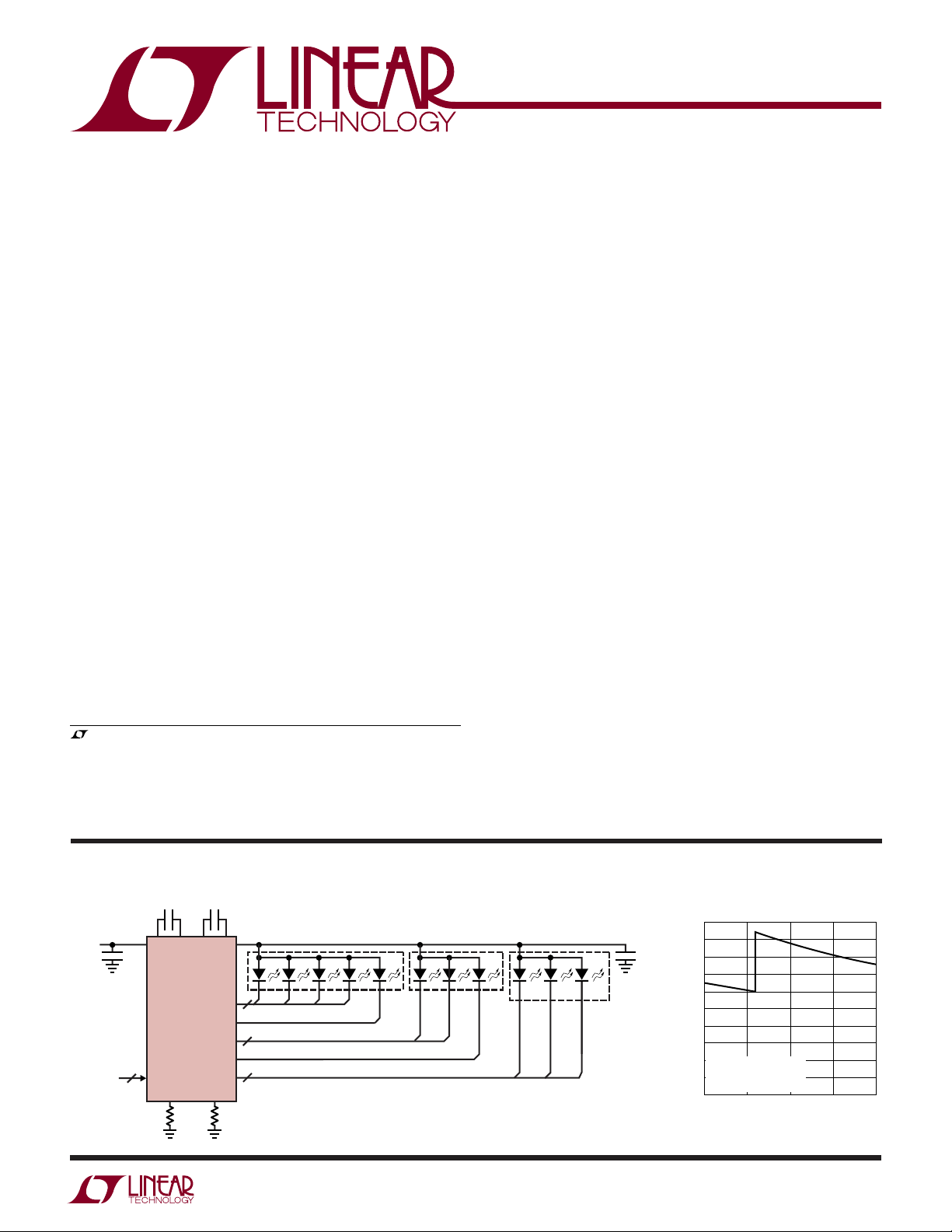
TYPICAL APPLICATIO
2.2µF 2.2µF
V
IN
2.7V TO
4.5V
I2C SERIAL
INTERFACE
V
IN
2.2µF 2.2µF
2
SERIAL PORT
I
RGB
LTC3206
CPO
MAIN1-4
AUX 1
SUB1-2
AUX 2
RGB
I
MS
4
2
3
U
MAIN DISPLAY SUB DISPLAY RGB ILLUMINATOR
RED GREEN BLUE
3206 TA01a
5-LED Main Display Efficiency
vs Input Voltage
100
90
80
) (%)
70
IN
/P
60
LED
50
40
30
EFFICIENCY (P
20
FIVE LEDs AT 15mA/LED
AT 15mA = 3.2V)
(TYP V
F
10
= 25°C
T
A
0
3.0
3.6
3.3
INPUT VOLTAGE (V)
3.9
4.2
3206 TA01b
3206f
1
LTC3206
24 23 22 21 20 19
7 8 9
TOP VIEW
25
UF PACKAGE
24-LEAD (4mm × 4mm) PLASTIC QFN
10 11 12
13
14
15
16
17
18
6
5
4
3
2
1
SUB1
SUB2
C2
–
C1
–
C1
+
C2
+
BLUE
GREEN
RED
V
IN
CPO
SGND
AUX2
AUX1
MAIN1
MAIN2
MAIN3
MAIN4
DV
CC
SDA
SCL
ENRGB/S
I
MS
I
RGB
ABSOLUTE AXI U RATI GS
(Note 1)
VIN, DVCC, CPO to GND............................... –0.3V to 6V
SDA, SCL, ENRGB/S ................. – 0.3V to (DV
I
(Continuous) (Note 4) ................................ 400mA
CPO
(Pulsed at 10% Duty Cycle) (Note 4)..................... 1A
I
MAIN1-4, ISUB1,2
(Pulsed at 10% Duty Cycle) (Note 4).............. 125mA
I
RED,GREEN,BLUE
(Pulsed at 10% Duty Cycle) (Note 4).............. 125mA
I
, I
MS
CPO Short-Circuit Duration ............................ Indefinite
Operating Temperature Range (Note 2) .. – 40°C to 85°C
Storage Temperature Range ................. –65°C to 125°C
ELECTRICAL CHARACTERISTICS
temperature range, otherwise specifications are at TA = 25°C. VIN = 3.6V, DVCC = 3V unless otherwise noted.
SYMBOL PARAMETER CONDITIONS MIN TYP MAX UNITS
Input Power Supply
White LED Current (MAIN1-MAIN4, SUB1, SUB2, AUX1, AUX2)
RGB LED Current (RED, GREEN, BLUE)
Charge Pump (CPO)
2
WW
W
U
UUW
PACKAGE/ORDER I FOR ATIO
ORDER PART
+ 0.3V)
CC
, I
AUX 1, 2
(Note 4) ..................... 100mA
(Note 4) ..................................... 100mA
(Note 4) .................................................. 1mA
RGB
T
= 125°C, θJA = 37°C/W, θJC = 2°C/W
JMAX
EXPOSED PAD IS PGND (PIN 25)
MUST BE SOLDERED TO PCB
Consult LTC Marketing for parts specified with wider operating temperature ranges.
The ● denotes the specifications which apply over the full operating
VIN Operating Voltage ● 2.7 4.5 V
DVCC Operating Voltage ● 1.5 5.5 V
VIN Operating Current I
DVCC Operating Current Serial Port Idle 1 µA
VIN Shutdown Current 7.3 10 µA
DVCC Shutdown Current 1 µA
IMS Servo Voltage 25µA < IMS < 75µA 0.585 0.6 0.615 V
Full-Scale LED Current Ratio (I
LED/IMS
LED Dropout Voltage 1.5x Mode Switch Threshold, I
LED Brightness Range 0.78 100 %
LED Current Matching MAIN-MAIN, MAIN-AUX, SUB-SUB, SUB-AUX 1 %
I
Servo Voltage 25µA < I
RGB
LED Current Ratio (I
) RED, GREEN, BLUE Voltage = 1V 360 400 440 mA/mA
LED/IRGB
RGB LED Dropout Voltage 1.5x Mode Switch Threshold, I
RGB PWM (Duty Factor) Range 0/15 15/15 %
1x Mode Output Impedance 0.68 Ω
1.5x Mode Output Impedance VIN = 3V, V
I
CPO
CPO
= IMS = I
= IMS = I
= 0µA, Direct-Connect Mode 180 µA
RGB
= 0µA, 1.5x Step-Up Mode 3.9 mA
RGB
● 0.582 0.6 0.618 V
) MAIN1-MAIN4, SUB1, SUB2, AUX1, AUX2, Voltage = 1V ● 368 400 432 mA/mA
= 20mA 80 mV
LED
< 75µA 0.585 0.6 0.615 V
RGB
= 20mA 80 mV
LED
= 4.2V (Note 3) 1.90 Ω
CPO
● 0.582 0.6 0.618 V
NUMBER
LTC3206EUF
UF PART
MARKING
3206
3206f
LTC3206
ELECTRICAL CHARACTERISTICS
temperature range, otherwise specifications are at T
The ● denotes the specifications which apply over the full operating
= 25°C. VIN = 3.6V, DVCC = 3V unless otherwise noted.
A
SYMBOL PARAMETER CONDITIONS MIN TYP MAX UNITS
CPO Regulation Voltage I
= 20mA, 1.5x Mode 4.75 V
CPO
CLK Frequency 0.68 0.96 1.36 MHz
SDA, SCL, ENRGB/S
V
IL
V
IH
I
IH
I
IL
V
OL
Low Level Input Voltage ● 0.3 • DV
High Level Input Voltage ● 0.7 • DV
Input Current SDA, SCL, ENRGB/S = DV
CC
CC
–1 1 µA
CC
Input Current SDA, SCL, ENRGB/S = 0V –1 1 µA
Digital Output Low (SDA) I
= 3mA ● 0.4 V
PULLUP
Timing Characteristics (Note 5)
t
SCL
t
BUF
t
HD, STA
t
SU, STA
t
SU, STD
t
HD, DAT(OUT)
t
HD, DAT(IN)
t
SU, DAT
t
LOW
t
HIGH
t
f
t
r
t
SP
Note 1: Absolute Maximum Ratings are those values beyond which the life
of a device may be impaired.
Note 2: The LTC3206E is guaranteed to meet performance specifications
from 0°C to 70°C. Specifications over the –40°C to 85°C operating
temperature range are assured by design, characterization and correlation
Clock Operating Frequency 400 kHz
Bus Free Time Between Stop and Start Condition 1.3 µs
Hold Time After (Repeated) Start Condition 0.6 µs
Repeated Start Condition Setup Time 0.6 µs
Stop Condition Setup Time 0.6 µs
Data Hold Time 225 900 ns
Input Data Hold Time 0 900 ns
Data Setup Time 100 ns
Clock Low Period 1.3 µs
Clock High Period 0.6 µs
Clock Data Fall Time 20 300 ns
Clock Data RiseTime 20 300 ns
Spike Suppression Time 50 ns
with statistical process controls.
Note 3: 1.5x mode output impedance is defined as (1.5VIN – V
CPO
)/I
OUT
.
Note 4: Based on long term current density limitations.
Note 5: All values are referenced to V
and V
IH
levels.
IL
V
V
UW
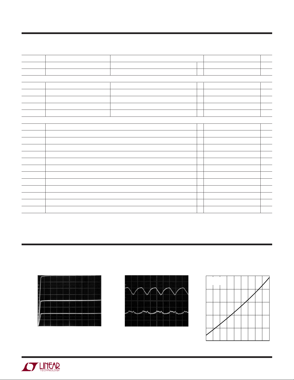
TYPICAL PERFOR A CE CHARACTERISTICS
I
LED
2.5mA/DIV
0mA
LED Pin Sink Current
vs LED Pin Voltage
100%
50%
25%
200mV/DIV 3206 G01 I
V
AT CURRENT SOURCE PIN
LED
AC COUPLED
(50mV/DIV)
AC COUPLED
(50mV/DIV)
Input and Output
Charge Pump Noise
CPO
V
IN
= 200mA 500ns/DIV 3206 G02
CPO
VIN = 3.6V
= C
= 1.6µF
C
IN
CPO
LED Pin Dropout Voltage
vs LED Pin Current
500
VIN = 3.6V
= 25°C
T
A
400
300
200
100
LED PIN DROPOUT VOLTAGE (mV)
0
10 30
20
50 90
60
40
LED CURRENT (mA)
70
80
100
3206 GO3
3206f
3
LTC3206
UW
TYPICAL PERFOR A CE CHARACTERISTICS
1.5x Mode Charge Pump Open1x Mode Switch Resistance
vs Temperature
0.9
I
= 100mA
CPO
0.8
VIN = 3.6V
0.7
0.6
SWITCH RESISTANCE (Ω)
0.5
–40
–15
10
TEMPERATURE (°C)
V
IN
= 3.3V
VIN = 3.9V
35
60
85
3206 G04
Loop Output Resistance vs
Temperature (1.5V
2.50
VIN = 3V
= 4.2V
V
CPO
= C
= C
= C
FLY1
TEMPERATURE (°C)
OUTPUT RESISTANCE (Ω)
2.25
2.00
1.75
1.50
C
IN
CPO
–15 10 35 60
–40
FLY2
– V
IN
= 1.6µF
CPO
)/I
CPO
3206 G05
1.5x Mode CPO Voltage
vs Load Current
4.8
4.7
4.6
4.5
4.4
4.3
4.2
CPO VOLTAGE (V)
4.1
4.0
3.9
85
3.8
0
CIN = C
3.1V
VIN = 3V
100
LOAD CURRENT (mA)
200
CPO
3.2V
= C
3.3V
FLY1 CFLY2
3.6V
300
400
T
A
= 1.6µF
= 25°C
3.5V
3.4V
3206 G06
500
Oscillator Frequency
vs Supply Voltage
1100
1000
TA = –40°C
900
FREQUENCY (kHz)
800
700
2.7
3.0 3.3 3.6 3.9
TA = 25°C
VIN SUPPLY VOLTAGE (V)
1x Mode No Load Supply Current
vs Input Voltage
300
TA = 25°C
= I
= 0µA
I
MS
RGB
250
200
SUPPLY CURRENT (µA)
150
TA = 85°C
4.2 4.5
3206 G07
DVCC Shutdown Current
vs Input Voltage
0.5
VIN = 3.6V
0.4
TA = –40°C
3.0
TA = 25°C
3.3 3.6 3.9
DVCC VOLTAGE (V)
SHUTDOWN CURRENT (µA)
DV
0.3
0.2
CC
0.1
0
2.7
1.5x Mode Supply Current
vs I
(IIN – 1.5I
CPO
10
VIN = 3.6V
= 25°C
T
A
8
6
4
SUPPLY CURRENT (mA)
2
CPO
)
TA = 85°C
4.2 4.5
3206 G08
VIN Shutdown Current
vs Input Voltage
10
DVCC = 3V
8
TA = –40°C
6
4
SHUTDOWN CURRENT (µA)
IN
2
V
0
2.7
3.0
TA = 25°C
3.3 3.6 3.9
INPUT VOLTAGE (V)
LED Pin Voltage for Higher LED
Currents
120
VIN = 3.6V
= 25°C
T
A
100
80
60
40
LED CURRENT (mA)
20
IMS, I
IMS, I
IMS, I
IMS, I
IMS, I
TA = 85°C
= 250µA
RGB
= 200µA
RGB
= 150µA
RGB
= 100µA
RGB
= 50µA
RGB
4.2 4.5
3206 G09
4
100
2.7
3.0 3.3 3.6 3.9
INPUT VOLTAGE (V)
4.2 4.5
3206 G10
0
0
100 150 200
50
LOAD CURRENT (mA)
250 300
3206 G11
0
0
0.4 0.6 0.8
0.2
LED PIN VOLTAGE (V)
1.0
3206 G12
3206f

LTC3206
U
UU
PI FU CTIO S
SUB1, SUB2 (Pins 1, 2): Current Source Outputs for the
SUB Display White LEDs. The current for the SUB display
is controlled by the resistor on the I
SUB display can be set to exponentially increasing brightness levels from 0.78% to 100% of full-scale. See Table 1.
C1+, C1–, C2+, C2– (Pins 5, 4, 6, 3): Charge Pump Flying
Capacitor Pins. A 2.2µF X7R or X5R ceramic capacitor
should be connected from C1
+
to C2–.
C2
DV
(Pin 7): This pin sets the logic reference level of the
CC
SDA, SCL and ENRGB/S pins.
SDA (Pin 8): Input Data for the I2C Serial Port. Serial data
is shifted in one bit per clock to control the LTC3206 (see
Figures 3 and 4). The logic level for SDA is referenced to
DVCC.
SCL (Pin 9): Clock Input for the I2C Serial Port (see Figures
3 and 4). The logic level for SCL is referenced to DVCC.
ENRGB/S (Pin 10): This pin is used to enable and disable
either the RED, GREEN and BLUE current sources or the
SUB display depending on which is programmed to respond via the I2C port. Once ENRGB/S is brought high, the
LTC3206 illuminates the RGB or SUB display with the
color combination or intensity that was previously programmed via the I2C port. The logic level for ENRGB/S is
referenced to DVCC.
IMS (Pin 11): This pin controls the maximum amount of
LED current in both the MAIN and SUB LED displays. The
IMS pin servos to 0.6V when there is a resistor to ground.
The full scale (100%) currents in the MAIN and SUB
display LEDs will be 400 times the current at the IMS pin.
I
(Pin 12): This pin controls the amount of LED current
RGB
at the RED, GREEN and BLUE LED pins. The I
servos to 0.6V when there is a resistor to ground. The
current in the RED, GREEN and BLUE LEDs will be 400
times the current at the I
scale.
+
pin when programmed to full
RGB
pin.The LEDs on the
MS
to C1– and another from
pin
RGB
CPO (Pin 14): Output of the Charge Pump. This output
should be used to power white, blue and “true” green
LEDs. Red LEDs can be powered from V
or X7R low impedance (ceramic) 2.2µF charge storage
capacitor is required on CPO.
VIN (Pin 15): Supply Voltage for the Charge Pump. The V
pin should be connected directly to the battery and bypassed with a 2.2µF X5R or X7R ceramic capacitor.
RED, GREEN, BLUE (Pins 16, 17, 18): Current Source
Outputs for the RGB Illuminator LEDs. The currents for the
RGB LEDs are controlled by the resistor on the I
The RGB LEDs can independently be set to any duty cycle
from 0/15 through 15/15 under software control giving a
total of 16 shades per LED and 4096 colors for the
illuminator. See Table 1. The RGB LEDs are modulated at
1/240 the speed of the charge pump oscillator (approximately 4kHz).
MAIN1-MAIN4 (Pins 22, 21, 20, 19): Current Source
Outputs for the Main Display White LEDs. The current for
the main display is controlled by the resistor on the I
pin. The LEDs on the MAIN display can be set to 16
exponentially increasing brightness steps from 0.78% to
100% of full scale. See Table 1.
AUX1, AUX2 (Pins 23, 24): Current source outputs for the
auxiliary white LEDs. The auxiliary current sources can be
individually assigned to be either MAIN display or SUB
display LEDs via the I2C serial port. When either AUX1 and/
or AUX2 are assigned to the MAIN display they will have
the same power setting as the other MAIN LEDs. Likewise,
when either AUX1 and/or AUX2 are assigned to the SUB
display they will have the same power setting as the other
SUB LEDs. The currents for the AUX1 and AUX2 pins are
controlled by the resistor on the IMS pin.
PGND (Pin 25, Exposed Pad): Power Ground for the
Charge Pump. This pin should be connected directly to a
low impedance ground plane.
or CPO. An X5R
IN
pin.
RGB
IN
MS
SGND (Pin 13): Ground for the control logic. This pin
should be connected directly to a low impedance ground
plane.
3206f
5

LTC3206
BLOCK DIAGRA
W
I
I
RGB
SGND
C1+C1–C2+C2
5 4 6 3
960kHz
OSCILLATOR
V
15
IN
1x AND 1.5x CHARGE PUMP
–
PGND
25
CPO
14
–
+
+
–
11
MS
+
–
12
13
ENABLECP
MAIN1
22
MAIN2
21
MAIN3
20
MAIN4
19
AUX1
23
AUX2
24
2
2
SUB1
1
SUB2
2
2
DV
7
ENRGB/S
SDA
SCL
CC
10
8
9
STOP
CONTROL
LOGIC
4 4 4244 4
COMMAND LATCH
I2C SERIAL PORT
PWM
U
OPERATIO
Power Management
To optimize efficiency, the power management section of
the LTC3206 provides two methods of supplying power to
the CPO pin: 1x direct connect mode or 1.5x boost mode.
When any display of the LTC3206 is enabled, the power
management system connects the CPO pin directly to V
with a low impedance switch. If the voltage supplied at V
is high enough to power all of the LEDs with the programmed current, the system will remain in this “direct
connect” mode providing maximum efficiency. Internal
IN
IN
RED
16
GREEN
17
BLUE
18
3206 BD
circuits monitor all current sources for the onset of “dropout,” the point at which the current sources can no longer
supply programmed current. As the battery voltage falls,
the LED with the largest forward voltage will reach the dropout threshold first. When any of the LED pins reach the dropout threshold, the LTC3206 will switch to boost mode and
automatically soft-start the 1.5x boost charge pump. The
constant frequency charge pump is designed to minimize
the amount of noise generated at the VIN supply.
3206f
6

OPERATIO
LTC3206
U
The 1.5x step-up charge pump uses a patented constant
frequency architecture to combine the best efficiency with
the maximum available power at the lowest noise level.
The charge pump of the LTC3206 can be forced to come
on even if no LEDs are programmed for current. Setting bit
2
A3 in the I
C serial port forces the charge pump on (see
Figure 3).
Soft-Start
To prevent excessive inrush current and supply droop
when switching into step-up mode, the LTC3206 employs
a soft-start feature on its charge pump. The current
available to the CPO pin is increased linearly over a period
of about 400µs.
Charge Pump Strength
When the LTC3206 operates in 1.5x boost mode, the
charge pump can be modeled as a Thevenin-equivalent
circuit to determine the amount of current available from
the effective input voltage, 1.5V
and the effective open-
IN
loop output resistance, ROL (Figure 1).
ROL is dependent on a number of factors including the
switching term, 1/(2f
OSC
• C
), internal switch resis-
FLY
tances and the non-overlap period of the switching circuit.
However, for a given ROL, the amount of current available
will be directly proportional to the advantage voltage 1.5V
– V
. Consider the example of driving white LEDs from
CPO
IN
a 3.1V supply. If the LED forward voltage is 3.8V and the
current sources require 100mV, the advantage voltage is
3.1V • 1.5 – 3.8V – 0.1V or 750mV. Notice that if the input
voltage is raised to 3.2V, the advantage voltage jumps to
900mV—a 20% improvement in available strength.
From Figure 1, the available current is given by:
VV
15.–
I
OUT
=
IN CPO
R
OL
R
OL
+
1.5V
IN
–
3206 F01
Figure 1. Equivalent Open-Loop Circuit
+
CPO
–
Typical values of ROL as a function of temperature are
shown in Figure 2.
2.50
VIN = 3V
= 4.2V
V
CPO
= C
= C
= C
C
IN
CPO
2.25
2.00
1.75
OUTPUT RESISTANCE (Ω)
1.50
–40
Figure 2. Typical ROL vs Temperature
FLY1
–15 10 35 60
TEMPERATURE (°C)
FLY2
= 1.6µF
85
3206 F02
I2C Interface
The LTC3206 communicates with a host (master) using
the standard I2C 2-wire interface. The Timing Diagram
(Figure 4) shows the timing relationship of the signals on
the bus. The two bus lines, SDA and SCL, must be high
when the bus is not in use. External pull-up resistors or
current sources, such as the LTC1694 SMBus accelerator,
are required on these lines. The LTC3206 is a receive-only
(slave) device.
Bus Speed
The I2C port is designed to be operated at speeds of up to
400kHz. It has built-in timing delays to ensure correct
operation when addressed from an I2C compliant master
device. It also contains input filters designed to suppress
glitches should the bus become corrupted.
START and STOP Conditions
A bus-master signals the beginning of a communication to
a slave device by transmitting a START condition. A
START condition is generated by transitioning SDA from
high to low while SCL is high. When the master has
finished communicating with the slave, it issues a STOP
condition by transitioning SDA from low to high while SCL
is high. The bus is then free for communication with
another I2C device.
3206f
7

LTC3206
OPERATIO
U
Byte Format
Each byte sent to the LTC3206 must be 8 bits long followed
by an extra clock cycle for the Acknowledge bit to be
returned by the LTC3206. The data should be sent to the
LTC3206 most significant bit (MSB) first.
Acknowledge
The Acknowledge bit is used for handshaking between the
master and the slave. An Acknowledge (active LOW)
generated by the slave (LTC3206) lets the master know
that the latest byte of information was received. The
Acknowledge related clock pulse is generated by the
master. The master releases the SDA line (HIGH) during
the Acknowledge clock cycle. The slave-receiver must pull
down the SDA line during the Acknowledge clock pulse so
that it remains a stable LOW during the HIGH period of this
clock pulse.
Slave Address
The LTC3206 responds to only one 7-bit address which
has been factory programmed to 0011011. The eighth bit
of the address byte (R/W) must be 0 for the LTC3206 to
recognize the address since it is a write only device. This
is equivalent to an 8-bit address where the least significant
bit of the address is always 0. If the correct seven bit
address is given but the R/W bit is 1, the LTC3206 will not
respond.
Bus Write Operation
The master initiates communication with the LTC3206
with a START condition and a 7-bit address followed by the
Write Bit R/W = 0. If the address matches that of the
LTC3206, the LTC3206 returns an Acknowledge. The
master should then deliver the most significant data byte.
Again the LTC3206 acknowledges and the cycle is repeated two more times for a total of one address byte and
three data bytes. Each data byte is transferred to an
internal holding latch upon the return of an Acknowledge.
After all three data bytes have been transferred to the
LTC3206, the master may terminate the communication
with a STOP condition. Alternatively, a REPEAT-START
condition can be initiated by the master and another chip
on the I2C bus can be addressed. This cycle can continue
indefinitely and the LTC3206 will remember the last input
of valid data that it received. Once all chips on the bus have
been addressed and sent valid data, a STOP condition can
be sent and the LTC3206 will update its command latch
with the data that it had received.
In certain circumstances, the data on the I
become corrupted. In these cases the LTC3206 responds
appropriately by preserving only the last set of complete
data that it has received. For example, assume the LTC3206
has been successfully addressed and is receiving data
when a STOP condition mistakenly occurs. The LTC3206
will ignore this stop condition and will not respond until a
new START condition, correct address, new set of data
and STOP condition are transmitted.
Likewise, if the LTC3206 was previously addressed and
sent valid data but not updated with a STOP, it will respond
to any STOP that appears on the bus independent of the
number of REPEAT-STARTs that have occurred. An exception occurs if a REPEAT-START is given and the
LTC3206 successfully acknowledges its addressed. In
this case, it will not respond to a STOP after the first data
byte is acknowledged. It will, however, respond after the
third data byte is acknowledged.
2
C bus may
8
3206f

UWW
ACK ACK
123
ADDRESS WR
456789123456789123456789123456789
00110 110
00110110
A7 A6 A5 A4 A3 A2 A1 A0
A7 A6 A5 A4 A3 A2 A1 A0 B7 B6 B5 B4 B3 B2 B1 B0
B7 B6 B5 B4 B3 B2 B1 B0
C7 C6 C5 C4 C3 C2 C1 C0
C7 C6 C5 C4 C3 C2 C1 C0
ACK
STOPSTART
SDA
SCL
ACK
FORCE
CHARGE PUMP
ENSUB_ENRGB
AUXSEL1
AUXSEL0
RED
BLUE
GREEN
MAIN
SUB
3206 FO3
t
SU, DAT
t
HD, STA
t
HD, DAT
SDA
SCL
t
SU, STA
t
HD, STA
t
SU, STO
3206 F04
t
BUF
t
LOW
t
HIGH
START
CONDITION
REPEATED START
CONDITION
STOP
CONDITION
START
CONDITION
t
r
t
f
t
SP
RED
GREEN
BLUE
MAIN
SUB
HEX
0
1
2
3
4
5
6
7
8
9
A
B
C
D
E
F
A7
B3
B7
C7
C3
0
0
0
0
0
0
0
0
1
1
1
1
1
1
1
1
A4
B0
B4
C4
C0
0
1
0
1
0
1
0
1
0
1
0
1
0
1
0
1
A6
B2
B6
C6
C2
0
0
0
0
1
1
1
1
0
0
0
0
1
1
1
1
A5
B1
B5
C5
C1
0
0
1
1
0
0
1
1
0
0
1
1
0
0
1
1
4-BIT CODE SUB-RANGE
NA
1/4
1/4
1/4
1/4
1/4
1/4
1/4
1/4
1/4
1/4
1/4
1/2
1/2
1
1
DUTY CYCLE
NA
3.13%
4.42%
6.25%
8.80%
12.50%
17.70%
25.00%
35.35%
50.00%
70.70%
100.00%
70.70%
100.00%
70.70%
100.00%
BRIGHTNESS
LEVEL
OFF
0.78%
1.07%
1.56%
2.25%
3.13%
4.40%
6.25%
8.90%
12.50%
17.70%
25.00%
35.35%
50.00%
70.70%
100.00%
BRIGHTNESS
LEVEL
OFF
1/15(6.7%)
2/15(13.3%)
3/15(20.0%)
4/15(26.7%)
5/15(33.3%)
6/15(40.0%)
7/15(46.7%)
8/15(53.3%)
9/15(60.0%)
10/15(66.6%)
11/15(73.3%)
12/15(80.0%)
13/15(86.7%)
14/15(93.3%)
15/15(100.0%)
MAIN
SUB
AUX
RED
GREEN
BLUE
A0
0
0
1
1
A1
0
1
0
1
AUX1
MAIN
MAIN
SUB
SUB
AUX2
MAIN
SUB
MAIN
SUB
A2
0
1
CONTROL
RGB DISPLAY
SUB DISPLAY
TI I G DIAGRA
LTC3206
Figure 3. Bit Assignments
Table 3. ENRGB/S Assignment
Table 2. Auxilliary LED Pin Assignments
Figure 4. Timing Parameters
Table 1. Serial Port Bit Assignments
3206f
9

LTC3206
WUUU
APPLICATIO S I FOR ATIO
White LED Brightness Control
The White LED displays (MAIN, SUB and AUX) have 16
individual brightness settings. The settings are exponentially spaced to compensate for the nearly logarithmic
characteristic of human vision perception. The base of the
power settings is √2 . The off setting (0 power) is a special
case needed for shutdown.
The LTC3206 uses a subranging technique to control the
LED brightness with a combination of both DC level
control and pulse width modulation. Table 1 summarizes
the level control operation. The DC level of the LEDs will be
one of either three sub-range settings, 100%, 50% or 25%
of full scale. For example, if the full scale LED current is
programmed (via the IMS pin) to be 20mA, then the “on”
level of the LED will be either 20mA, 10mA or 5mA
respectively. The power to the LED will be the product of
the subrange (DC current) and the PWM setting. For
example, if an LED power of 2.25% is desired, then the
LTC3206 sets the sub range to 25% and the duty cycle to
8.8%. These settings are designed to optimize the efficiency of the dual-mode LTC3206 power management
system while preserving LED color accuracy at low power
levels.
To achieve brightness control by purely DC means, only
the 100%, 50% or 25% power settings should be selected.
The DC current levels of the MAIN, SUB and AUX LEDs are
controlled by a precisely mirrored multiple of the current
at the IMS pin. The IMS pin servos to a fixed level of 0.6V so
the current is programmed simply by adding a resistor
from IMS to ground.
The current that flows during the “on” time will follow the
relationship:
V
IS
= 40006••
LED
where S is the subrange for the given power setting (it will
be either 25%, 50% or 100%, see Table 1) and RMS is the
value of the resistor at the IMS pin.
The average LED current (LED power level) will follow the
relationship:
.
R
MS
D
AVG I
() •.•=−400
LED
06
R
MS
V
15
2
where D is the decimal equivalent of the 4-bit digital code
programmed for the given display (0 to 15).
The PWM frequency is 1/1024 of the frequency of the
charge pump oscillator (typically 938Hz). During PWM,
the LED currents are soft-switched to minimize noise.
AUX LEDs
The AUX1 and AUX2 LEDs can be arbitrarily assigned to
either the MAIN or SUB display. Table 2 summarizes the
assignment possibilities. When an AUX pin is assigned to
a display, it will follow the power level (both DC and PWM)
set for that display.
Unused White LED Pins
The LTC3206 can power up to eight white LEDs (four for
the MAIN display, two for the SUB display and the two
flexible AUX pins), however, it is not necessary to use all
eight in each application.
Any of these LED pins can cause the LTC3206 to switch
from 1x mode to 1.5x charge pump mode if they drop out.
In fact, if an unused LED pin is left unconnected or
grounded, it
will
drop out and force the LTC3206 into
charge pump mode.
To avoid this problem, unused MAIN, SUB or AUX LED
pins can be disabled by connecting them to CPO. Power is
not wasted in this configuration. When the LED pin voltage
is within approximately 1V of CPO, its LED current is
switched off and only a small 10µA test current remains.
Figure 5 shows a block diagram of each of the MAIN, SUB
and AUX LED pins.
CPO
1V
+
+
–
MAIN1-MAIN4
SUB1, SUB2, AUX1, AUX2
–
ENABLE
I
LED
Figure 5. Internal MAIN, SUB and AUX LED Disable Circuit
10µA
3206 F05
3206f
10

WUUU
APPLICATIO S I FOR ATIO
LTC3206
The RED, GREEN and BLUE pins can also enable the
charge pump, however, since they each have individual
disable control they can be left floating or grounded if
unused.
RGB Illuminator Brightness Control
The RED, GREEN and BLUE LEDs can be individually set
to have a linear duty cycle ranging from 0/15 (off) to
15/15 (full on) with 1/15 increments in between. The
combination of 16 possible brightness levels gives the
RGB indicator LED a total of 4096 colors. Table 1 indicates
the decoding of the RED, GREEN and BLUE LEDs.
The full-scale currents in the RED, GREEN and BLUE LEDs
are controlled by the current at the I
pin in a similar
RGB
manner to those in the MAIN, SUB and AUX LEDs. The
I
pin also servos to 0.6V and the RGB LED currents are
RGB
a precise multiple of the I
current. The DC value of the
RGB
RGB display LED currents will follow the relationship:
.
06
R
RGB
V
pin.
RGB
I
RED GREENBLUE
,,
where R
RGB
= 400
is the value of the resistor at the I
The average value of the current in the RED, GREEN and
BLUE LEDs will be:
(see Figure 3 and Table 3) determines which display
ENRGB/S controls. When bit A2 is 0, the ENRGB/S pin
controls the RGB display. If it is set to 1, ENRGB/S controls
the SUB display.
To use the ENRGB/S pin, the I2C port must first be
configured to the desired setting. For example, if ENRGB/S
will be used to control the SUB display, then a non-zero
code must reside in the C3-C0 nibble of the I2C port and bit
A2 must be set to 1 (see Table 1). Now when ENRGB/S is
high (DVCC), the SUB display will be on with the C3-C0
setting. When ENRGB/S is low, the SUB display will be off.
If no other displays are programmed to be on, the entire
chip will be in shutdown.
Likewise, if ENRGB/S will be used to enable the RGB
display, then a non-zero code must reside in one of the
RED, GREEN or BLUE nibbles of the serial port (A4-A7 or
B0-B7), and bit A2 must be 0. Now when ENRGB/S is high
(DVCC), the RGB display will light with the programmed
color. When ENRGB/S is low, the RGB display will be off.
If no other displays are programmed to be on, the entire
chip will be in shutdown.
If bit A2 is set to 1 (SUB display control), then ENRGB/S
will have no effect on the RGB display. Likewise, if bit A2
is set to 0 (RGB display control), then ENRGB/S will have
no effect on the SUB display.
DV
.
AVG I
()••
RED GREENBLUE
,,
= 400
15
06
R
RGB
where D is the decimal equivalent of the 4-bit digital code
programmed for the given LED(0 to 15). Table 1 summarizes the RED, GREEN and BLUE LED power settings.
The RED, GREEN and BLUE LEDs are pulse width modulated at a frequency of 1/240 of the frequency of the charge
pump oscillator or about 4kHz.
ENRGB/S Pin
The ENRGB/S pin can be used to enable or disable the
LTC3206 without re-accessing the I2C port. This might be
useful to indicate an incoming phone call without waking
the microcontroller. ENRGB/S can be software programmed as an independent control for either the RGB
display or the SUB display. Control bit A2 in the serial port
If the ENRGB/S pin is not used, it should be connected to
DVCC. It should not be grounded or left floating.
VIN, CPO Capacitor Selection
The style and value of capacitors used with the LTC3206
determine several important parameters such as regulator
control-loop stability, output ripple and charge pump
strength. To reduce noise and ripple, it is recommended
that low equivalent series resistance (ESR) multilayer
ceramic capacitors be used on both VIN and CPO. Tantalum and aluminum capacitors are not recommended because of their high ESR. The value of the capacitor on CPO
directly controls the amount of output ripple for a given
load current. Increasing the size of this capacitor will
reduce the output ripple. The peak-to-peak output ripple is
approximately given by the expression:
I
V
RIPPLE
P-P
≅
CPO
fC
3•
OSC CPO
3206f
11

LTC3206
WUUU
APPLICATIO S I FOR ATIO
where f
960kHz) and C
is the LTC3206’s oscillator frequency (typically
OSC
is the output charge storage capacitor
CPO
on CPO. Both the style and value of the output capacitor
can significantly affect the stability of the LTC3206. The
LTC3206 uses a linear control loop to adjust the strength
of the charge pump to match the current required at the
output. The error signal of this loop is stored directly on
the output charge storage capacitor. The charge storage
capacitor also serves to form the dominant pole for the
control loop. To prevent ringing or instability, it is important for the output capacitor to maintain at least 0.6µF of
capacitance over all conditions. Likewise, excessive ESR
on the output capacitor will tend to degrade the loop
stability of the LTC3206. The closed-loop output resistance of the LTC3206 is designed to be 0.4Ω. For a 100mA
load current change, the error signal will change by about
40mV. If the output capacitor has 0.4Ω or more of ESR,
the closed-loop frequency response will cease to roll off in
a simple one-pole fashion and poor load transient response or instability could result. Multilayer ceramic chip
capacitors typically have exceptional ESR performance.
MLCC capacitors combined with a tight board layout, will
yield very good stability. As the value of C
controls the
CPO
amount of output ripple, the value of CIN controls the
amount of ripple present at the input pin (VIN). The input
current to the LTC3206 will be relatively constant while the
charge pump is on either the input charging phase or the
output charging phase but will drop to zero during the
clock nonoverlap times. Since the non-overlap time is
small (~25ns), these missing “notches” will result in only
a small perturbation on the input power supply line. Note
that a higher ESR capacitor such as tantalum will have
higher input noise due to the input current change times
the ESR. Therefore, ceramic capacitors are again recommended for their exceptional ESR performance. Input
noise can be further reduced by powering the LTC3206
through a very small series inductor as shown in Figure 6.
A 10nH inductor will reject the fast current notches,
thereby presenting a nearly constant current load to the
input power supply. For economy, the 10nH inductor can
be fabricated on the PC board with about 1cm (0.4") of PC
board trace.
Flying Capacitor Selection
10nH
V
IN
Figure 6. 10nH Inductor Used for Input Noise
Reduction (Approximately 1cm of Wire)
V
IN
2.2µF0.1µF
LTC3206
GND
3206 F06
Warning: A polarized capacitor such as tantalum or aluminum should never be used for the flying capacitors since
their voltage can reverse upon start-up of the LTC3206.
Ceramic capacitors should always be used for the flying
capacitors.
The flying capacitor controls the strength of the charge
pump. In order to achieve the rated output current it is
necessary to have at least 1µF of capacitance for each of
the flying capacitors. Capacitors of different materials lose
their capacitance with higher temperature and voltage at
different rates. For example, a ceramic capacitor made of
X7R material will retain most of its capacitance from
–40°C to 85°C whereas a Z5U or Y5V style capacitor will
lose considerable capacitance over that range. Z5U and
Y5V capacitors may also have a very poor voltage coefficient causing them to lose 60% or more of their capacitance when the rated voltage is applied. Therefore, when
comparing different capacitors, it is often more appropriate to compare the amount of achievable capacitance for
a given case size rather than comparing the specified
capacitance value. For example, over rated voltage and
temperature conditions, a 1µF, 10V, Y5V ceramic capaci-
tor in a 0603 case may not provide any more capacitance
than a 0.22µF, 10V, X7R available in the same 0603 case.
The capacitor manufacturer’s data sheet should be consulted to determine what value of capacitor is needed to
ensure minimum capacitances at all temperatures and
voltages.
12
3206f

WUUU
GND
V
IN
CPO
3206 F07
PIN 1
APPLICATIO S I FOR ATIO
Table 4 shows a list of ceramic capacitor manufacturers
and how to contact them:
Table 4. Recommended Capacitor Vendors
AVX www.avxcorp.com
Kemet www.kemet.com
Murata www.murata.com
Taiyo Yuden www.t-yuden.com
Vishay www.vishay.com
For very light load applications, the flying capacitors
may be reduced to save space or cost. The theoretical
minimum output resistance of a 1.5x fractional charge
pump is given by:
.–
15 1
VV
R
OL MIN
where f
C
is the value of the flying capacitors. Note that the
FLY
≡ =
()
is the switching frequency (960kHz typ) and
OSC
charge pump will typically be weaker than the theoretical
limit due to additional switch resistance, however for very
light load applications, the above expression can be used
as a guideline in determining a starting capacitor value.
Layout Considerations and Noise
Due to its high switching frequency and the transient
currents produced by the LTC3206, careful board layout is
necessary. A true ground plane and short connections to
all capacitors will improve performance and ensure proper
regulation under all conditions. Figure 7 shows the recommended layout configuration.
The flying capacitor pins C1+, C2+, C1– and C2– will have
very high edge rate waveforms. The large dv/dt on these pins
can couple energy capacitively to adjacent printed circuit
board runs. Magnetic fields can also be generated if the
flying capacitors are not close to the LTC3206 (i.e., the loop
area is large). To decouple capacitive energy transfer, a
Faraday shield may be used. This is a grounded PC trace
between the sensitive node and the LTC3206 pins. For a high
quality AC ground, it should be returned to a solid ground
plane that extends all the way to the LTC3206.
IN OUT
IfC
OUT OSC FLY
2
LTC3206
Figure 7. Optimum Single Layer PCB Layout
Power Efficiency
To calculate the power efficiency (η) of a white LED driver
chip, the LED power should be compared to the input
power. The difference between these two number represents lost power whether it is in the charge pump or the
current sources. Stated mathematically, the power efficiency is given by:
P
LED
η≡
P
IN
The efficiency of the LTC3206 depends upon the mode in
which it is operating. Recall that the LTC3206 operates as
a pass switch, connecting VIN to CPO until one of the LEDs
drops out. This feature provides the optimum efficiency
available for a given input voltage and LED forward voltage. When it is operating as a switch, the efficiency is
approximated by:
P
LED
η≡ = ≅
P
IN
since the input current will be very close to the LED
current.
At moderate to high output power, the quiescent current
of the LTC3206 is negligible and the expression above is
valid. For example, with VIN = 3.9V, I
and V
equal to 3.6V, the measured efficiency is 92.2%,
LED
which is very close to the theoretical 92.3% calculation.
•
VI
LED LED
•
VIVV
IN IN
LED
IN
= 20mA • 6 LEDs
OUT
3206f
13

LTC3206
WUUU
APPLICATIO S I FOR ATIO
Once an LED pin drops out, the LTC3206 switches into
step-up mode. Employing the fractional ratio 1.5x charge
pump, the LTC3206 provides more efficiency than would
be achieved with a voltage doubling charge pump.
In 1.5x boost mode, the efficiency is similar to that of a
linear regulator with an effective input voltage of 1.5 times
the actual input voltage. This is because the input current
for a 1.5x fractional charge pump is approximately 1.5
times the load current. In an ideal 1.5x charge pump, the
power efficiency would be given by:
P
η
IDEAL
LED
≡ = ≅
P
Thermal Management
For higher input voltages and maximum output current,
there can be substantial power dissipation in the LTC3206.
If the junction temperature increases above approximately
160°C the thermal shutdown circuitry will automatically
deactivate the output. To reduce the maximum junction
temperature, a good thermal connection to the PC board
is recommended. Connecting the PGND pin (exposed
center pad) to a ground plane and maintaining a solid
ground plane under the device can reduce the thermal
resistance of the package and PC board considerably.
Brightness Control
Although the LTC3206 has many exponentially spaced
brightness settings for the main and sub displays, it is
possible to control the brightness by alternative means.
Figure 8 shows an example of how an external voltage
source can be use to inject a current into the IMS or I
pins to control brightness. For example, if R1 and R2 are
24k, then the LED current would range from 20mA to 0mA
as V
is swept from 0V to 1.2V.
CNTRL
Alternatively, if only digital outputs are available, the
number of settings can be doubled from 15 to 30 by simply
VI
•
LED LED
VIVV
IN
•. .15 15
IN LED
LED
IN
RGB
V
0.6V
CNTRL
–
||
R2
R1
3206 F08
R2
R2
V
CNTRL
R1
LTC3206
I
I
MS
RGB
I
= 400
LED
()
11
12
12k
Figure 8. Alternative Linear Brightness Control
connecting V
to a digital signal. This topology can be
CNTRL
extended to any number of bits and can also be applied to
the RGB display.
Finally, PWM brightness control can be achieved by apply-
LTC3206
I
I
RGB
MS
11
12
12k
Figure 9. Alternative Digital Brightness Control
18.2k
3206 F09
34k
V
DIG
0V TO 0.7V
OR HIGHER
ing a PWM signal to the IMS programming resistor as
shown in Figure 10. The signal should range from 0V (full
on) to any voltage above 0.7V (full off).
LTC3206
I
I
RGB
Figure 10. PWM Brightness Control of the MAIN and SUB Displays
MS
12k
11
12k
12
PWM SIGNAL
0V TO 0.7V OR HIGHER
BRIGHTNESS = 1 – D
3206 F10
14
3206f

TYPICAL APPLICATIO S
2.2µF2.2µF
V
IN
2.7V TO
2.7V TO
4.5V
4.5V
I2C SERIAL
INTERFACE
V
IN
V
IN
2.2µF 2.2µF
LTC3206
MAIN1-4
AUX 1
AUX 2
I
RGB
12k 12k
SUB1-2
RGB
I
MS
2
SERIAL PORT
Main Backlight, Keypad Backlight Plus Motor Controller
2.2µF2.2µF
V
IN
2.2µF 2.2µF
CPO
LTC3206
U
CPO
4-Display Controller
MAIN DISPLAY SUB DISPLAY ILLUMINATOR
4
2
3
MAIN DISPLAY KEYPAD
RED GREEN BLUE
FLASH
CAMERA
LIGHT
3206 TA02
LTC3206
MAIN1-4
AUX 1-2
SUB1-2
R
I
MS
12k 12k
G
I2C SERIAL
INTERFACE
2
SERIAL PORT
I
RGB
PACKAGE DESCRIPTIO
4.50 ± 0.05
3.10 ± 0.05
2.45 ± 0.05
(4 SIDES)
RECOMMENDED SOLDER PAD PITCH AND DIMENSIONS
B
0.25 ±0.05
0.50 BSC
8
U
UF Package
24-Lead Plastic QFN (4mm × 4mm)
(Reference LTC DWG # 05-08-1692)
4.00 ± 0.10
(4 SIDES)
0.70 ±0.05
PACKAGE
OUTLINE
PIN 1
TOP MARK
(NOTE 5)
NOTE:
1. DRAWING PROPOSED TO BE MADE A JEDEC PACKAGE OUTLINE MO-220 VARIATION (WGGD-X)—TO BE APPROVED
2. ALL DIMENSIONS ARE IN MILLIMETERS
3. DIMENSIONS OF EXPOSED PAD ON BOTTOM OF PACKAGE DO NOT INCLUDE
MOLD FLASH. MOLD FLASH, IF PRESENT, SHALL NOT EXCEED 0.15mm ON ANY SIDE, IF PRESENT
4. EXPOSED PAD SHALL BE SOLDER PLATED
5. SHADED AREA IS ONLY A REFERENCE FOR PIN 1 LOCATION
ON THE TOP AND BOTTOM OF PACKAGE
6. DRAWING NOT TO SCALE
0.75 ± 0.05
2.45 ± 0.10
(4-SIDES)
0.200 REF
0.00 – 0.05
BATT
VIBRATOR
MOTOR
3206 TA04
BOTTOM VIEW—EXPOSED PAD
R = 0.115
TYP
(4 SIDES)
24
23
0.23 TYP
0.38 ± 0.10
1
2
(UF24) QFN 0603
0.25 ± 0.05
0.50 BSC
3206f
Information furnished by Linear Technology Corporation is believed to be accurate and reliable.
However, no responsibility is assumed for its use. Linear Technology Corporation makes no representation that the interconnection of its circuits as described herein will not infringe on existing patent rights.
15

LTC3206
TYPICAL APPLICATIO
U
5-LED Main Plus Low/High Current Camera Light
2.2µF 2.2µF
V
2.7V TO
4.5V
I2C SERIAL
INTERFACE
IN
FLASH
V
IN
2.2µF 2.2µF
LTC3206
ENRGB/S
2
SERIAL PORT
I
RGB
2.4k 12k
CPO
MAIN1-4
AUX 1
AUX 2
SUB1-2
RGB
I
MS
4
3
3
MAIN DISPLAY
TORCH MODE
FLASH MODE
HIGH CURRENT
CAMERA LED
3206 TA03
RELATED PARTS
PART NUMBER DESCRIPTION COMMENTS
LT®1618 Constant Current, Constant Voltage, 1.4MHz Up to 16 White LEDs, VIN: 1.6V to 18V, V
High Efficiency Boost Regulator I
LTC1911-1.5 250mA (I
), 1.5MHz High Efficiency 75% Efficiency, VIN: 2.7V to 5.5V, V
OUT
≤1µA, 10-Lead MS Package
SD
OUT(MIN)
Step-Down Charge Pump ISD ≤10µA, MS8 Package
LT1932 Constant Current, 1.2MHz High Efficiency White Up to 8 White LEDs, VIN: 1V to 10V, V
LED Boost Regulator ThinSOT
TM
Package
LT1937 Constant Current, 1.2MHz High Efficiency White Up to 4 White LEDs, VIN: 2.5V to 10V, V
LED Boost Regulator I
≤1µA, ThinSOT, SC70 Packages
SD
LTC3200-5 Low Noise, 2MHz Regulated Charge Pump Up to 6 White LEDs, VIN: 2.7V to 4.5V, V
OUT(MAX)
OUT(MAX)
OUT(MAX)
White LED Driver ThinSOT Package
LTC3201 Low Noise, 1.7MHz Regulated Charge Pump Up to 6 White LEDs, VIN: 2.7V to 4.5V, V
OUT(MAX)
White LED Driver 10-Lead MS
LTC3202 Low Noise, 1.5MHz Regulated Charge Pump Up to 8 White LEDs, VIN: 2.7V to 4.5V, V
OUT(MAX)
White LED Driver 10-Lead MS Package
LTC3205 Multi-Display LED Controller 92% Efficiency, VIN: 2.8V to 4.5V, IQ = 50µA, ISD ≤ 1µA ,
4mm × 4mm QFN Package
LTC3251 500mA (I
Step-Down Charge Pump I
LTC3405/LTC3405A 300mA (I
), 1MHz to 1.6MHz Spread Spectrum 85% Efficiency, VIN: 3.1V to 5.5V, V
OUT
), 1.5MHz Synchronous Step-Down 95% Efficiency, VIN: 2.7V to 6V, V
OUT
≤1µA, 10-Lead MS Package
SD
: 0.9V to 1.6V, IQ = 9µA,
OUT
OUT(MIN)
DC/DC Converter ThinSOT Package
LTC3406/LTC3406B 600mA (I
), 1.5MHz Synchronous Step-Down 95% Efficiency, VIN: 2.5V to 5.5V, V
OUT
OUT(MIN)
DC/DC Converter ThinSOT Package
LTC3440 600mA (I
), 2MHz Synchronous Buck-Boost 95% Efficiency, VIN: 2.5V to 5.5V, V
OUT
OUT(MIN)
DC/DC Converter 10-Lead MS Package
LT3465/LT3465A 1.2MHz/2.7MHz with Internal Schottky Up to 6 White LEDs, VIN: 12.7V to 16V, V
<1µA, ThinSOT Package
I
SD
ThinSOT is a trademark of Linear Technology Corporation.
= 34V, IQ = 1.8mA,
OUT(MAX)
= 1.5V/1.8V, IQ = 180µA,
= 34V, IQ = 1.2mA, IS ≤1µA,
= 34V, IQ = 1.9mA,
= 5V, IQ = 8mA, ISD ≤1µA,
= 5V, IQ = 6.5mA, ISD ≤1µA,
= 5V, IQ = 5mA, ISD ≤1µA,
= 0.8V, IQ = 20µA, ISD ≤1µA,
= 0.6V, IQ = 20µA, ISD ≤1µA,
= 2.5V, IQ = 25µA, ISD ≤1µA,
= 34V, IQ = 1.9mA,
OUT(MAX)
16
Linear Technology Corporation
1630 McCarthy Blvd., Milpitas, CA 95035-7417
(408) 432-1900 ● FAX: (408) 434-0507 ● www.linear.com
3206f
LT/TP 0604 1K • PRINTED IN USA
© LINEAR TECHNOLOGY CORPORATION 2004
 Loading...