

FEATURES
LTC2926
MOSFET-Controlled
Power Supply Tracker
U
DESCRIPTIO
■
Flexible Power Supply Tracking and Sequencing
■
Adjustable Ramp Rates, Offsets and Time Delays
■
Controls Three Supplies with Series MOSFETs
■
Integrated Remote Sense Switching
■
FAULT Input/Output
■
STATUS Output/Power Good Input
■
Available in 20-Lead Narrow SSOP and 20-Lead QFN
(4mm × 5mm) Packages
U
APPLICATIO S
■
V
■
Microprocessor, DSP and FPGA Supplies
■
Servers
■
Communications Systems
All other trademarks are the property of their respective owners.
*Protected by U.S. Patents including 6897717.
and V
CORE
, LT, LTC and LTM are registered trademarks of Linear Technology Corporation.
Supply Tracking
I/O
U
TYPICAL APPLICATIO
1.8V MODULE
OUT
SENSE
3.3V MODULE
OUT
SENSE
15.0k
4.02k
FAULT
ON/OFF
100Ω
100Ω
15.0k
9.53k
10k
0.1µF
V
CC
D1
D2
RAMPBUF
TRACK1
TRACK2
V
CC
FAULT
ON
IRF7413Z
10Ω
SGATE2
LTC2926
GND
IRF7413Z
10Ω
PGTMR
SGATE1
STATUS/PGI
MGATE
RAMP
2926 TA01
1µF
FB1
FB2
1.8V
SLAVE1
3.3V
SLAVE2
S1
15.0k
9.53k
S2
15.0k
V
CC
4.02k
10k
STATUS
0.1µF
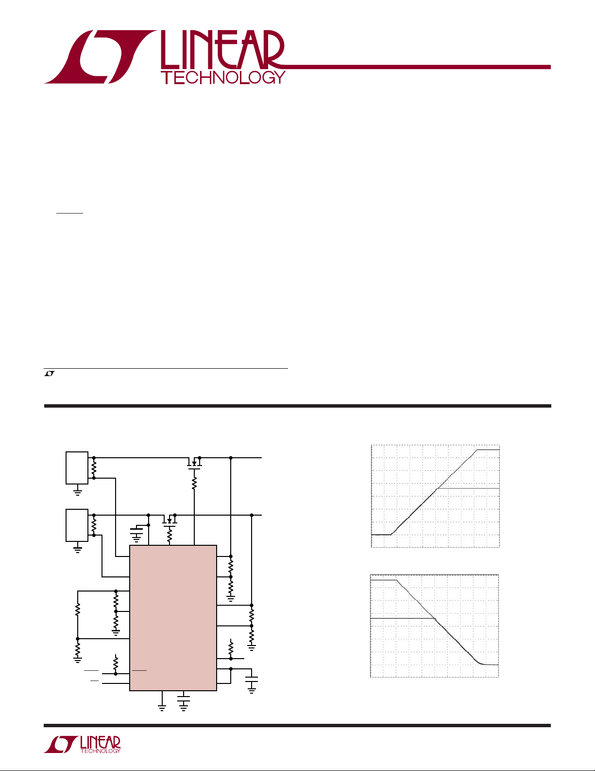
The LTC2926 provides a simple solution for tracking and
sequencing up to three power supply rails. An N-channel
MOSFET and a few resistors per channel confi gure the
load voltages to ramp up and down together, with voltage
offsets, with time delays or with different ramp rates.
Automatic remote sense switching compensates for voltage
drops across the MOSFETs. The LTC2926 provides two
integrated switches as well as a signal to control optional
additional external N-channel MOSFET sense switches.
The LTC2926 includes I/O signals for communication with
other devices. The status output asserts after tracking and
sequencing have completed. A low voltage on the power
good input after an adjustable timeout period causes load
disconnect. A low voltage on the fault I/O causes immediate load disconnect. Until it is reset, a fault latch prevents
tracking and keeps the loads disconnected.
3.3V SLAVE2
500mV/DIV
5ms/DIV
3.3V SLAVE2
1.8V SLAVE1
5ms/DIV
1.8V SLAVE1
2926 TA01b
500mV/DIV
2926 TA01c
2926fa
1
LTC2926
WW
W
U
ABSOLUTE AXI U RATI GS
(Notes 1, 2)
Supply Voltage (VCC) ................................. –0.3V to 10V
Input Voltages
ON ......................................................... –0.3V to 10V
RAMP .............................................–0.3V to V
TRACK1, TRACK2 ........................–0.3V to V
PGTMR ........................................–0.3V to V
CC
+ 0.3V
CC
+ 0.3V
CC
+ 1V
Input/Output Voltages
FAULT .................................................... –0.3V to 10V
STATUS/PGI (Note 3) .......................... –0.3V to 11.5V
Output Voltages
RAMPBUF ....................................–0.3V to V
+ 0.3V
CC
FB1, FB2, D1, S1, D2, S2 ....................... –0.3V to 10V
MGATE, RSGATE (Note 3) ................... –0.3V to 11.5V
SGATE1, SGATE2 (Note 3) .................. –0.3V to 11.5V
UUW
PACKAGE/ORDER I FOR ATIO
RMS Currents
TRACK1, TRACK2 ................................................5mA
FB1, FB2 ..............................................................5mA
D1, S1, D2, S2 ...................................................30mA
Operating Temperature
LTC2926C ................................................ 0°C to 70°C
LTC2926I ............................................. –40°C to 85°C
Storage Temperature Range
GN Package .......................................–65°C to 150°C
UFD Package ...................................... –65°C to 125°C
Lead Temperature (Soldering, 10 sec)
GN Package ......................................................300°C
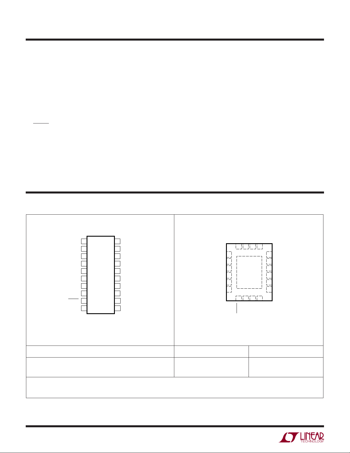
TOP VIEW
1
V
CC
TRACK1
SGATE1
2
3
FB1
4
S1
5
6
D1
7
ON
8
PGTMR
9
FAULT
10
GND
20-LEAD PLASTIC SSOP
T
JMAX
GN PACKAGE
= 125°C, θJA = 85°C/W
RAMPBUF
20
TRACK2
19
FB2
18
S2
17
SGATE2
16
D2
15
STATUS/PGI
14
RSGATE
13
MGATE
12
RAMP
11
ORDER PART NUMBER ORDER PART NUMBER UFD PART MARKING*
LTC2926CGN
LTC2926IGN
Order Options Tape and Reel: Add #TR
Lead Free: Add #PBF Lead Free Tape and Reel: Add #TRPBF
Lead Free Part Marking: http://www.linear.com/leadfree/
TOP VIEW
TRACK1
VCCRAMPBUF
TRACK2
20 19 18 17
9 10
RAMP
16
15
14
13
12
11
MGATE
FB2
S2
SGATE2
D2
STATUS/PGI
RSGATE
2926
2926
1
FB1
S1
2
SGATE1
3
4
D1
ON
5
6
PGTMR
20-LEAD (4mm × 5mm) PLASTIC QFN
EXPOSED PAD (PIN 21) IS GND
PCB CONNECTION OPTIONAL
T
JMAX
21
7 8
GND
FAULT
UFD PACKAGE
= 125°C, θJA = 43°C/W
LTC2926CUFD
LTC2926IUFD
Consult LTC Marketing for parts specifi ed with wider operating temperature ranges.*The temperature grade is identifi ed by a label on the shipping container.
2926fa
2
LTC2926
ELECTRICAL CHARACTERISTICS
The
temperature range, otherwise specifi cations are at T
SYMBOL PARAMETER CONDITIONS MIN TYP MAX UNITS
Supply Voltage
V
CC
I
CC
V
CC(UVLO)
ΔV
CC(UVLO)
Control and I/O
V
ON(TH)
ΔV
ON(TH)
I
ON
V
ON(CLR)
t
CLR
V
ON(ARM)
t
ARM
V
FAULT(TH)
I
FAULT(UP)
V
FAULT(OL)
V
FAULT(OH)
V
PGI(TH)
ΔV
PGI(TH)
I
PGI(UP)
V
STATUS(OL)
V
STATUS(OH)
V
PGTMR(TH)
I
PGTMR(UP)
I
PGTMR(DN)
V
PGTMR(CLR)
Ramp Buffer
I
RAMP(IN)
V
RAMPBUF(OS)
V
RAMPBUF(OL)
Input Supply Voltage Operating Range
Input Supply Current I
Input Supply Undervoltage Lockout VCC Rising
Input Supply Undervoltage Lockout
Hysteresis
ON Pin Threshold Voltage VON Rising
ON Pin Threshold Voltage Hysteresis
ON Pin Input Current VON = 1.2V, VCC = 5.5V
ON Pin Fault Clear Threshold Voltage VON Falling
Fault Clear Delay VON Falling
ON Pin Fault Arm Threshold Voltage VON Rising
Fault Arm Delay VON Rising
FAULT Pin Input Threshold Voltage V
FAULT Pin Pull-up Current Fault Latch Clear, V
FAULT Pin Output Low Voltage Fault Latch Set, I
FAULT Pin Output High Voltage
(V
CC
– V
FAULT
)
STATUS/PGI Pin Input Threshold
Voltage
STATUS/PGI Pin Input Threshold
Voltage Hysteresis
STATUS/PGI Pin Pull-Up Current STATUS/PGI On, V
STATUS/PGI Pin Output Low Voltage VON Low, I
STATUS/PGI Pin Output High Voltage
(V
STATUS/PGI
– VCC)
PGTMR Pin Threshold Voltage V
PGTMR Pin Pull-Up Current ON High, V
PGTMR Pin Pull-Down Current ON Low, V
PGTMR Pin Clear Threshold Voltage V
RAMP Pin Input Current 0V < V
Ramp Buffer Offset Voltage V
RAMPBUF Pin Output Low Voltage I
= 25°C. VCC = 3.3V unless otherwise specifi ed.
A
TRACKn
I
RAMPBUF
I
TRACKn
I
RAMPBUF
Fault Latch Clear, I
V
I
STATUS/PGI
RAMPBUF
= 0mA, I
= –1mA, I
= –3mA
Falling
FAULT
STATUS/PGI
Rising
PGTMR
Falling
PGTMR
RAMP
= 1/2 VCC, I
RAMP
= 3mA
●
denotes the specifi cations which apply over the full operating
●
2.9 3.3 5.5 V
= 0mA,
FBn
●
1.5 2.5 3.5 mA
= 0mA
= –1mA,
FBn
= 1.5V
FAULT
= 5mA, VCC = 2.7V
FAULT
= –1µA
FAULT
Rising
STATUS/PGI
STATUS/PGI
= 5mA, VCC = 2.7V
= –1µA
= 1V
PGTMR
= 0.1V, VCC = 2.7V
PGTMR
< 5.5V, VCC = 5.5V
RAMPBUF
= 1.5V
= 0mA
●
8.5 9.5 10.5 mA
●
2.2 2.4 2.6 V
●
15 50 75 mV
●
1.20 1.23 1.26 V
●
40 75 110 mV
●
●
0.465 0.500 0.535 V
●
1 3 10 µs
●
0.565 0.600 0.635 V
●
1 4.5 10 µs
●
0.465 0.500 0.535 V
●
–3.0 –8.5 –13 µA
●
●
300 550 900 mV
●
1.10 1.23 1.36 V
●
30 75 150 mV
●
–7 –10 –13 µA
●
●
5.0 5.5 6.0 V
●
1.10 1.23 1.36 V
●
–8 –10 –12 µA
●
0.5 4 10 mA
●
50 100 150 mV
●
●
●
0 ±100 nA
100 400 mV
200 400 mV
0±1 µA
0 ±10 mV
32 60 mV
2926fa
3

LTC2926
ELECTRICAL CHARACTERISTICS
The
temperature range, otherwise specifi cations are at T
SYMBOL PARAMETER CONDITIONS MIN TYP MAX UNITS
V
RAMPBUF(OH)
Tracking Channels
I
ERROR(%)
V
TRACK
V
FB(REF)
I
FB(LEAK)
V
FB(CLAMP)
Master Ramp and Supply
ΔV
MGATE
I
MGATE(UP)
I
MGATE(DN)
I
MGATE(FAULT)
Slave Supplies
ΔV
SGATE
I
SGATE(UP)
I
SGATE(DN)
I
SGATE(UPFST)
I
SGATE(DNFST)
I
SGATE(FAULT)
Remote Sense Switches
ΔV
RSGATE
I
RSGATE(UP)
I
RSGATE(DN)
I
RSGATE(FAULT)
V
RSGATE(TH)
R
SW(ON)
RAMPBUF Pin Output High Voltage
(V
– V
CC
I
to I
FBn
TRACKn
(I
– I
FBn
TRACKn
)
RAMPBUF
Current Mismatch
)/I
TRACKn
• 100%
TRACK Pins Voltage I
FB Pins Internal Reference Voltage V
FB Pins Leakage Current V
FB Pins Clamp Voltage –1mA < I
MGATE Pin External N-Channel Gate
Drive (V
MGATE
– VCC)
MGATE Pin Pull-Up Current Fault Latch Clear, VON High, V
MGATE Pin Pull-Down Current Fault Latch Clear, VON Low, V
MGATE Pin Fault Pull-Down Current Fault Latch Set, VON High, V
SGATE Pins External N-Channel Gate
Drive (V
SGATEn
– VCC)
SGATE Pins Pull-Up Current Fault Latch Clear, V
SGATE Pins Pull-Down Current Fault Latch Clear, V
SGATE Pins Fast Pull-Up Current Fault Latch Clear, V
SGATE Pins Fast Pull-Down Current Fault Latch Clear, V
SGATE Pins Fault Pull-Down Current Fault Latch Set, VON High, V
RSGATE Pin External N-Channel Gate
Drive (V
RSGATE
– VCC)
RSGATE Pin Pull-Up Current Fault Latch Clear, Switches On, V
RSGATE Pin Pull-Down Current Fault Latch Clear, Switches Off,
RSGATE Pin Fault Pull-Down Current Fault Latch Set, Switches Off,
RSGATE Pin Threshold Voltage Ramping Completed on Pin Low, RSGATE
Remote Sense Switch On-Resistance Switches On, VDn = VCC + 0.3V, ISn = –10mA
= 25°C. VCC = 3.3V unless otherwise specifi ed.
A
I
RAMPBUF
I
TRACKn
I
TRACKn
TRACKn
I
TRACKn
I
MGATE
V
I
SGATEn
V
V
V
I
RSGATE
V
V
Falling
●
denotes the specifi cations which apply over the full operating
= –3mA
= –10µA
= –1mA
= –10µA
= –1mA
= VCC, I
TRACKn
= 0.8V, VCC = 5.5V
FBn
< –1µA
FBn
= –1µA
= 5.5V
CC
= –1µA, V
= 3.3V
SGATEn
= 3.3V
SGATEn
= 5.5V
CC
= –1µA
= 3.3V
RSGATE
= 5.5V, VCC = 5.5V
RSGATE
FBn
FBn
= 0mA
= 0.75V
= V
FBn
= V
FBn
= 0V, V
FBn
= 1V, V
FBn
MGATE
MGATE
MGATE
FB(REF)
FB(REF)
SGATEn
SGATEn
SGATEn
= 3.3V
= 3.3V
= 5.5V,
– 10mV,
+ 10mV,
= 3.3V
= 3.3V
= 5.5V,
= 0V
RSGATE
●
●
●
●
0.776
●
0.776
●
0.784 0.800 0.816 V
●
●
1.7 2.0 2.4 V
●
5.0 5.5 6.0 V
●
–7 –10 –13 µA
●
71013 µA
●
52050 mA
●
5.0 5.5 6.0 V
●
–6 –10 –13 µA
●
61013 µA
●
–21 –30 –39 µA
●
21 30 39 µA
●
52050 mA
●
5.0 5.5 6.0 V
●
–7 –10 –13 µA
●
71013 µA
●
52050 mA
●
1.10 1.23 1.36 V
●
60 80 mV
0
0
0.800
0.800
±3
±3
0.824
0.824
0 ±10 nA
210
%
%
V
V
Ω
Note 1: Stresses beyond those listed under Absolute Maximum Ratings
may cause permanent damage to the device. Exposure to any Absolute
Maximum Rating condition for extended periods may affect device
reliability and lifetime.
Note 2: All currents into the device pins are positive; all currents out of
the device pins are negative. All voltages are referenced to ground unless
otherwise specifi ed.
4
Note 3: The MGATE, SGATE1, SGATE2, RSGATE and STATUS/PGI pins are
internally limited to a minimum of 11.5V. Driving these pins to voltages
beyond the clamp level may damage the part.
2926fa
LTC2926
UW
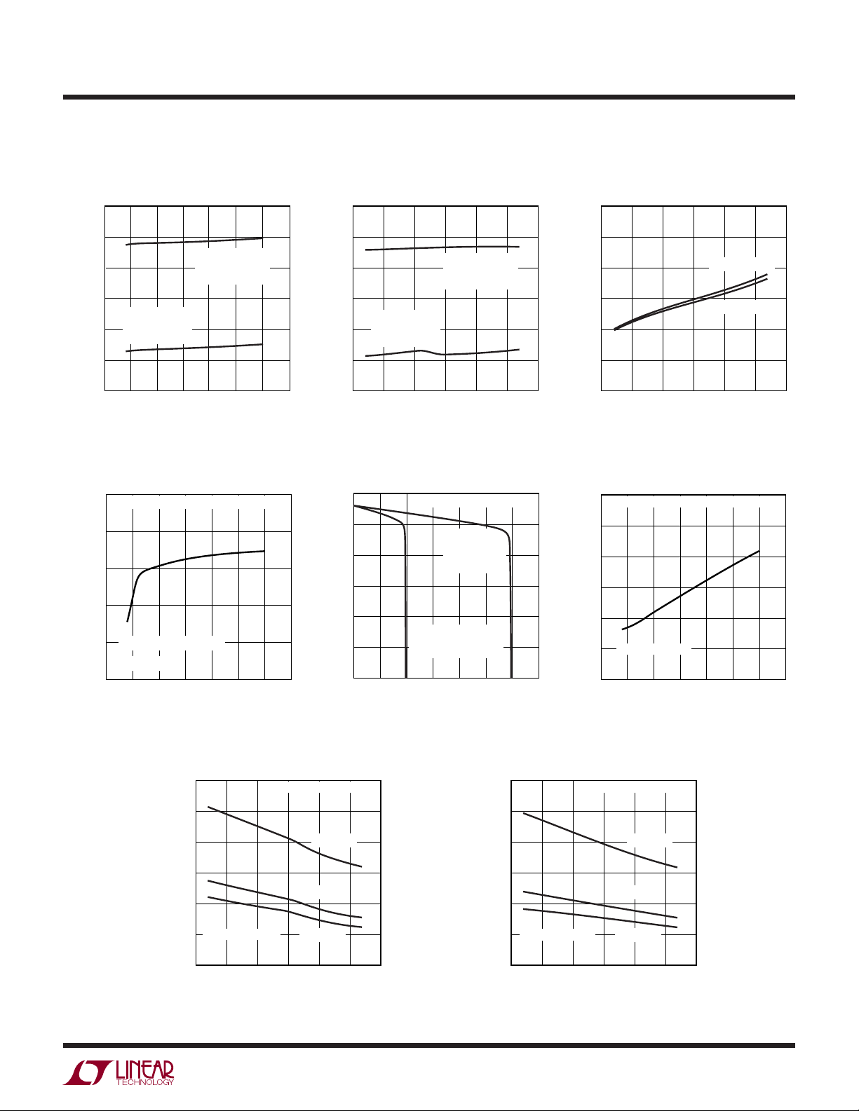
TYPICAL PERFOR A CE CHARACTERISTICS
Specifi cations are at TA = 25°C, VCC = 3.3V
unless otherwise specifi ed.
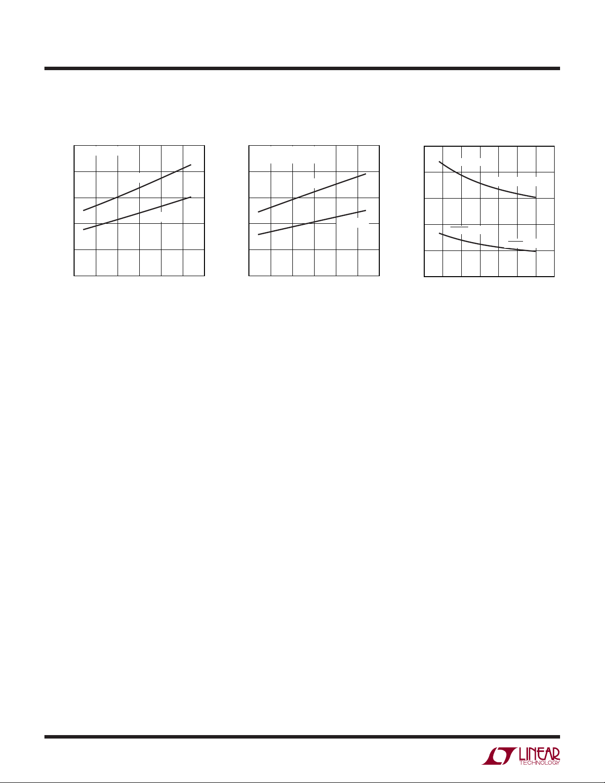
Supply Current vs Supply Voltage Supply Current vs Temperature Track Pin Voltage vs Temperature
12
12
0.812
10
8
6
(mA)
CC
I
I
= 0mA
RAMPBUF
= 0mA
I
TRACKn
4
2
0
= 0mA
I
FBn
3.0 3.5 4.5 5.5 6.0
2.5
Gate Drive Voltages vs
Supply Voltage
6.0
MGATE, RSGATE, SGATE1, SGATE2 PINS
5.8
5.6
5.4
GATE DRIVE (V)
5.2
GATE DRIVE = V
= –1µA
I
GATE
5.0
3.0 3.5 4.0 4.5 5.0 5.5
2.5
I
RAMPBUF
= –1mA
I
TRACKn
= –1mA
I
FBn
4.0 5.0
(V)
V
CC
– V
PIN
CC
VCC (V)
= –3mA
2926 G01
2926 G05
6.0
10
I
= –3mA
8
6
(mA)
CC
I
I
RAMPBUF
= 0mA
I
TRACKn
4
2
0
–50 25 75–25 0 50 100
I
FBn
= 0mA
RAMPBUF
I
TRACKn
= –1mA
I
FBn
= 0mA
TEMPERATURE (°C)
= –1mA
Gate Drive Voltages vs
Load Current
6
5
4
3
GATE DRIVE (V)
2
1
0
01525510 20 3530
GATE DRIVE = V
SGATE1,
SGATE2 PINS
FAST PULL-UP
MODE
MGATE, RSGATE,
SGATE1, SGATE2 PINS
PULL-UP MODE
I
(µA)
LOAD
PIN
2926 G02
– V
2926 G06
0.808
I
= –10µA
0.804
(V)
0.800
TRACK
V
0.796
0.792
0.788
–50 25 75–25 0 50 100
TEMPERATURE (°C)
TRACK
I
TRACK
= –1mA
2926 G03
Gate Fault Pull-Down Currents vs
Supply Voltage
30
CC
(mA)
GATE(PD)
I
MGATE, RSGATE, SGATE1, SGATE2 PINS
25
20
15
10
5
FAULT LATCH SET
0
3.0 3.5 4.0 4.5 5.0 5.5
2.5
(V)
V
CC
6.0
2926 G07
MGATE, RSGATE Fault Pull-Down
Currents vs Temperature
30
25
(mA)
20
15
RSGATE(PD)
, I
10
MGATE(PD)
I
5
FAULT LATCH SET
0
–50 25 75–25 0 50 100
MGATE, RSGATE PINS
VCC = 5.5V
VCC = 3.3V
VCC = 2.9V
TEMPERATURE (°C)
2926 G08
SGATE Fault Pull-Down Current vs
Temperature
30
25
20
(mA)
15
SGATE(PD)
I
10
5
FAULT LATCH SET
0
–50 25 75–25 0 50 100
SGATE1, SGATE2 PINS
VCC = 5.5V
VCC = 3.3V
VCC = 2.9V
TEMPERATURE (°C)
2926 G09
2926fa
5
LTC2926
UW
TYPICAL PERFOR A CE CHARACTERISTICS
Specifi cations are at TA = 25°C, VCC = 3.3V
unless otherwise specifi ed.
RAMPBUF Output Low Voltage vs
Temperature
50
I
= 3mA
RAMPBUF
40
30
(mV)
OL
V
20
10
0
–50 25 75–25 0 50 100
VCC = 2.9V
VCC = 5.5V
TEMPERATURE (°C)
2926 G10
RAMPBUF Output High Voltage vs
Temperature
100
I
= –3mA
RAMPBUF
= VCC – V
V
OH
80
60
(mV)
OH
V
40
20
0
–50 25 75–25 0 50 100
RAMPBUF
VCC = 2.9V
VCC = 5.5V
TEMPERATURE (°C)
2926 G11
Logic Output Low Voltages vs
Supply Voltage
250
STATUS/PGI PIN
200
150
(mV)
OL
V
100
50
0
2.5
FAULT PIN
3.0 3.5 4.0 4.5 5.0 5.5
VCC (V)
I
STATUS/PGI
I
FAULT
= 5mA
= 5mA
6.0
2926 G12
6
2926fa

UUU
PI FU CTIO S
LTC2926
GN/UFD Packages
D1, S1, D2, S2 (Pins 6, 4, 15, 17/Pins 4, 2, 13, 15):
Remote Sense Switches #1 and #2. A 10Ω (max) switch
connects each pair of pins (D1/S1 and D2/S2) after MGATE,
SGATE1 and SGATE2 are all fully enhanced (MGATE >
RAMP + 4.9V or RAMP > V
+ 4.9V). The switch can be used to compensate for
V
CC
the voltage drop across the external MOSFET that controls
a slave or the master supply. Connect the switch between
the load and the supply’s sense node. Before the external
MOSFET is fully enhanced, a resistor between the supply’s
output and sense nodes provides local feedback. When
the ON pin voltage is low, the switch will open before the
MGATE, SGATE1 and SGATE2 pins will ramp down. Leave
unused switch terminal pairs unconnected.
Exposed Pad (Pin 21, UFD Package Only): Exposed pad
may be left open or connected to device GND.
FAULT (Pin 9/Pin 7): Negative-Logic Fault Input/Output.
Under normal conditions the internal fault latch is not set
and an 8.5µA current pulls up FAULT to a diode drop below
. When the voltage at FAULT is pulled below 0.5V, a
V
CC
fault condition is latched and an internal N-channel MOSFET pulls FAULT to GND until the latch is reset. The fault
condition also pulls STATUS/PGI low, opens the remote
sense switches, and pulls MGATE, SGATE1 and SGATE2
to GND to disconnect the master and slave supplies from
their loads. Pulling STATUS/PGI below 1V after the power
good time-out delay also latches a fault. The fault latch is
reset when the ON pin voltage is below 0.5V, or when V
is undervoltage. The fault latch is armed when the ON pin
voltage exceeds 0.6V. To auto-retry after a fault, connect
FAULT to the ON pin. Leave the FAULT pin unconnected
if it is unused.
FB1, FB2 (Pins 3, 18/Pins 1, 16): Feedback Control Input/Outputs. Each FB pin connects to the feedback node
of a slave supply. Connect an FB pin to the tap point of a
resistive voltage divider between the source (load side)
of the external MOSFET and GND. For a slave supply with
an accessible feedback path, no external MOSFET may
be necessary. In that case, connect an FB pin to the tap
point of a resistive voltage divider between the supply
generator’s feedback node and GND. To prevent damage
, and SGATE1, SGATE2 >
CC
CC
to the slave supply, the FB pins will not force the slave’s
feedback node above 2.4V. In addition, it will not actively
sink current even when the LTC2926 is not powered. Tie
unused FB pins to GND.
GND (Pin 10/Pin 8): Device Ground.
MGATE (Pin 12/Pin 10): Master Gate Drive for External
N-Channel MOSFET/Master Ramp. When the ON pin is
high, an internal 10µA current charges the gate of an
external N-channel MOSFET. A capacitor from MGATE
to GND sets the master ramp rate. Add a 10Ω resistor
between the capacitor and the MOSFET’s gate to prevent
high frequency oscillations. An internal charge pump
guarantees that the MGATE pin voltage will pull up to
5.5V above V
MOSFETs are fully enhanced. When the ON pin is pulled
low, the MGATE pin is pulled to GND by a 10µA current
source. Upon a fault condition, the MGATE pin is pulled
low immediately with 20mA. To create a master ramp
signal without an external MOSFET, tie the MGATE pin to
the RAMP pin. A weak internal clamp on the RAMP pin
limits MGATE to V
pin unconnected if it is unused.
ON (Pin 7/Pin 5): On Control Input. The ON pin has
a threshold of 1.23V with 75mV of hysteresis. A high
causes 10µA to fl ow out of the MGATE pin, ramping up
the supplies. A low causes 10µA to fl ow into the MGATE
pin, ramping down the supplies. Pull the ON pin below
0.5V to reset the fault latch. Pull the ON pin above 0.6V
after a fault latch reset to arm the fault latch.
PGTMR (Pin 8/Pin 6): Power Good Timer. Connect an
external capacitor between PGTMR and GND to set the
Power Good Time-Out Delay. When the ON pin is above
1.23V, a 10µA current pulls up PGTMR to V
an internal N-channel MOSFET pulls PGTMR to GND. If
the voltage on PGTMR exceeds 1.23V and the voltage
on STATUS/PGI is not above 1.23V, a fault condition is
latched, the remote sense switches are opened, and FAULT,
STATUS/PGI, MGATE, SGATE1, SGATE2 and RSGATE will
be immediately pulled to GND. To disable the Power Good
Timer tie PGTMR to GND.
, which ensures that logic-level N-channel
CC
+ 1V in this case. Leave the MGATE
CC
, otherwise
CC
2926fa
7

LTC2926
PI FU CTIO S
UUU
GN/UFD Packages
RAMP (Pin 11/ Pin 9): Ramp Buffer Input. Connect the
RAMP pin to the master ramp signal to force the slave
supplies to track it. When the RAMP pin is connected to
the source of an external N-channel MOSFET, the slave
supplies track the MOSFET’s source, the master supply
voltage, as it ramps up and down. When a master supply
is not required, the RAMP pin can be tied directly to the
MGATE pin to form a master ramp voltage. In this confi guration, the supplies track the capacitor on the MGATE pin as
it is charged and discharged by the 10µA current source
that is controlled by the ON pin. The RAMP pin is weakly
clamped to V
a low impedance source to avoid sinking large currents
into the pin. Ground the RAMP pin if it is unused.
RAMPBUF (Pin 20/Pin 18): Ramp Buffer Output. The
RAMPBUF pin provides a low impedance buffered version of the signal on the RAMP pin. This buffered output
drives the resistive voltage dividers that connect to the
TRACK pins. Limit the capacitance at the RAMPBUF pin
to less than 100pF.
RSGATE (Pin 13/Pin 11): Gate Drive for Internal and
External N-Channel MOSFET Remote Sense Switches. A
remote sense path between a load and the sense input of
its supply generator automatically compensates for voltage
drops across the tracking MOSFET. After the series MOSFETs are fully enhanced, a 10µA current pulls up RSGATE.
An internal charge pump guarantees that RSGATE will
pull up to 5.5V above V
N-channel MOSFETs are fully enhanced. When the voltage
at RSGATE exceeds V
is released. When the ON pin is low, a 10µA current source
pulls RSGATE to GND. Supplies will not track down until
the RSGATE pin voltage falls below 1.23V, which ensures
that the remote sense switches open before the loads are
disconnected. Connect RSGATE to the gates of additional
external N-channel MOSFETs to create more remote sense
switches. Upon a fault condition, the RSGATE pin is pulled
low immediately with 20mA. Optionally connect a capacitor between RSGATE and GND to set the switch-on rate
or to add delay between switch closure and STATUS/PGI
assertion. Leave RSGATE unconnected if it is unused.
+ 1V. Do not drive RAMP above VCC with
CC
, which ensures that logic-level
CC
+ 4.9V, the STATUS/PGI pull-down
CC
SGATE1, SGATE2 (Pins 5, 16/Pins 3, 14): Slave Gate Controllers for External N-Channel MOSFETs. Each SGATE pin
ramps a slave supply by controlling the gate of an external
N-channel MOSFET so that its source terminal follows the
tracking profi le set by external resistors and the master
ramp. It is a good practice to add a 10Ω resistor between
this pin and the MOSFET’s gate to prevent high frequency
oscillations. An internal charge pump guarantees that the
SGATE pin voltage will pull up to 5.5V above V
ensures that logic-level N-channel MOSFETs are fully
enhanced. Leave unused SGATE pins unconnected.
STATUS/PGI (Pin 14/Pin 12): Status Output/Power Good
Input. A 10µA current pulls up STATUS/PGI when MGATE,
SGATE1 and SGATE2 are fully enhanced, and the remote
sense switches are closed, otherwise an internal N-channel
MOSFET pulls down STATUS/PGI. If the STATUS/PGI pin
is pulled below 1V after the power-good time-out delay
(see PGTMR pin description), the fault latch is set, and
MGATE, SGATE1, SGATE2 and RSGATE are all pulled low
immediately. An internal charge pump guarantees that the
STATUS/PGI pin voltage will pull up to 5.5V above V
An external pull-up resistor may be added to limit the
STATUS/PGI voltage to logic levels. Leave the STATUS/PGI
pin unconnected if it is unused.
TRACK1, TRACK2 (Pins 2, 19/Pins 20, 17): Tracking Control Inputs. A resistive voltage divider between RAMPBUF
and each TRACK pin determines the tracking profi le of
each supply channel. Each TRACK pin pulls up to 0.8V,
and the current supplied at TRACK is mirrored at FB. The
TRACK pins are capable of supplying at least 1mA when
= 2.9V. They may be capable of supplying up to 10mA
V
CC
when the supply is at 5.5V, so care should be taken not to
short this pin for extended periods. Limit the capacitance
at the TRACK pins to less than 25pF. Leave unused TRACK
pins unconnected.
(Pin 1/Pin 19): Positive Voltage Supply. Operating
V
CC
range is from 2.9V to 5.5V. An undervoltage lockout resets
the part when the supply is below 2.4V. V
bypassed to GND with a 0.1µF capacitor.
, which
CC
should be
CC
CC
.
8
2926fa
LTC2926
UU
W
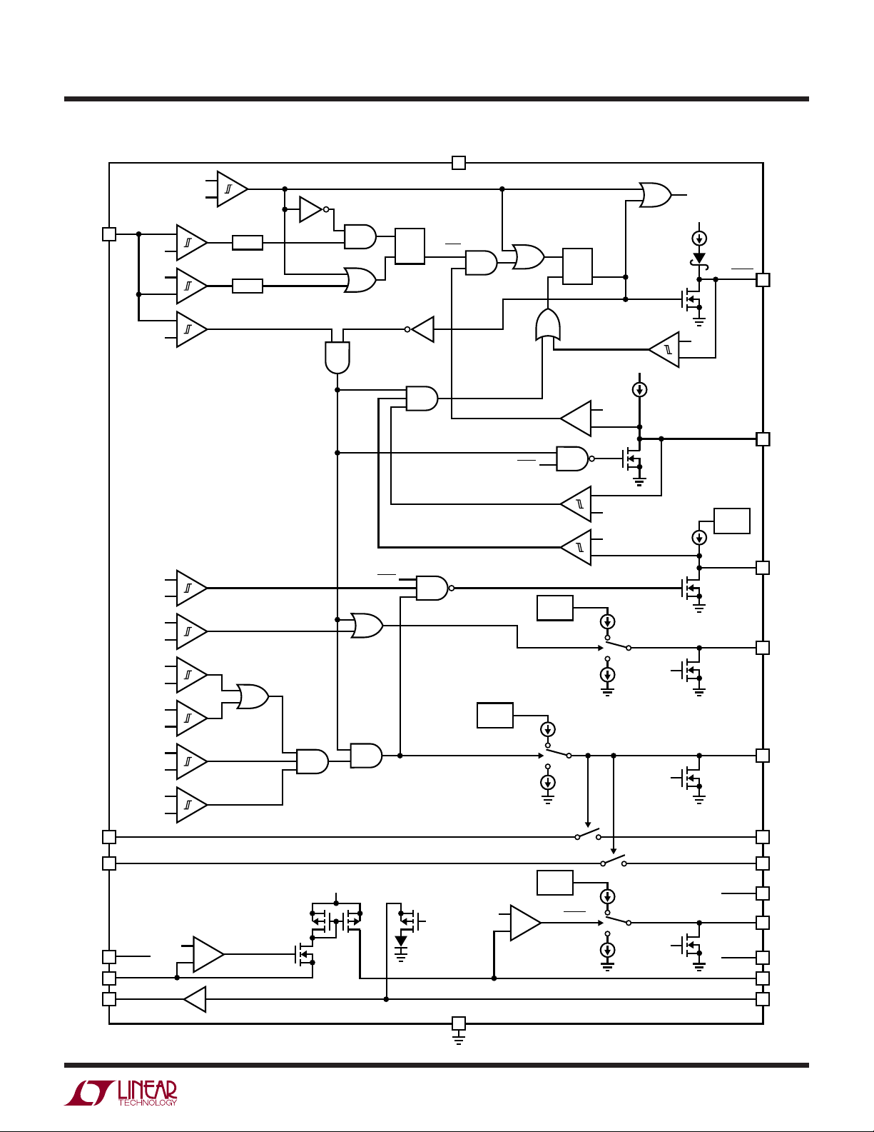
FU CTIO AL BLOCK DIAGRA
+
ON
0.6V
0.5V
1.23V
RSGATE
+ 4.9V
V
CC
RSGATE
1.23V
MGATE
RAMP + 4.9V
2.4V
V
CC
+
–
+
–
+
–
+
–
+
–
+
–
UVLO
–
DELAY
DELAY
UVLO
CLEAR/ARM
SIGNAL LATCH
R
SQ
CLR/ARM
V
CC
FAST PULL-DOWN
V
CC
8.5µA
FAULT
+
0.5V
–
V
CC
PGTMR
CHARGE
10µA
FAST
PUMP
STATUS/PGI
MGATEGATE UP
UVLO
PGTMR HIGH
PGI LOW
CHARGE
PUMP
FAULT LATCH
R
SQ
+
–
+
–
+
–
10µA
10µA
FAULT
10µA
0.1V
1.23V
1.23V
PULL-DOWN
RAMP
SGATE1
VCC + 4.9V
SGATE2
VCC + 4.9V
D1
D2
TRACK2
TRACK1
RAMPBUF
+
–
V
CC
+
–
+
–
V
CC
V
CC
+
0.8V
–
1x
GND
CHARGE
PUMP
0.8V
+
–
10µA
10µA
CHARGE
PUMP
10µA/30µA
FAST
PULL-DOWN
10µA/30µA
FAST
PULL-DOWN
RSGATERSGATE UP
S1
S2
SGATE2
SGATE1UP/DOWN
FB2
FB1
RAMP
2926 BD
2926fa
9

LTC2926
U
WUU
APPLICATIO S I FOR ATIO
Power Supply Tracking and Sequencing
The LTC2926 handles a variety of power-up profi les to
satisfy the requirements of digital logic circuits including
FPGAs, PLDs, DSPs and microprocessors. These requirements fall into one of the four general categories illustrated
in Figures 1 to 4.
Some applications require that the potential difference
between two power supplies must never exceed a specifi ed voltage. This requirement applies during power-up
and power-down as well as during steady-state operation,
often to prevent destructive latch-up in a dual supply IC.
Typically, this is achieved by ramping the supplies up
and down together (Figure 1). In other applications it is
desirable to have the supplies ramp up and down ratiometrically (Figure 2) or with fi xed voltage offsets between
them (Figure 3).
Certain applications require one supply to come up after
another. For example, a system clock may need to start
before a block of logic. In this case, the supplies are sequenced as in Figure 4, where the 1.8V supply ramps up
completely followed by the 2.5V supply.
Operation
The LTC2926 provides a simple solution to allow all of
the power supply tracking and sequencing profi les shown
in Figures 1 to 4. A single LTC2926 controls up to three
supplies: two “slave” supplies that track a “master” signal.
With just four resistors and an external N-channel MOSFET,
each slave supply is confi gured to ramp up and down as
a function of the master signal. This master signal can
be a third supply that is ramped up through an external
MOSFET, whose ramp rate is set with a single capacitor,
or it can be a signal generated by tying the MGATE and
RAMP pins together to an external capacitor.
Tracking Cell and Gate Controller Cell
The LTC2926’s operation is based on the combination of
a tracking cell and a gate controller cell that is shown in
Figure 5. The tracking cell servos the TRACK pin at 0.8V,
and the current supplied by the TRACK pin is mirrored at the
FB pin. The gate controller cell servos the FB pin at 0.8V by
driving the gate of the external N-channel MOSFET (Q
EXT
),
and establishes the slave output voltage at the source of
the MOSFET based on the TRACK pin current and resistors
500mV/DIV
500mV/DIV
5ms/DIV
5ms/DIV
2926 F01
2926 F03
MASTER
SLAVE2
SLAVE1
MASTER
SLAVE2
SLAVE1
500mV/DIV
500mV/DIV
SLAVE2
SLAVE1
5ms/DIV
Figure 2. Ratiometric TrackingFigure 1. Coincident Tracking
5ms/DIV
Figure 4. Supply SequencingFigure 3. Offset Tracking
2926 F02
SLAVE2
SLAVE1
2926 F04
2926fa
10

LTC2926
U
WUU
APPLICATIO S I FOR ATIO
SUPPLY
LTC2926 GATE CONTROLLER CELL
V
CC
MASTER
RAMP
R
TB
R
TA
TRACK
I
TRACK
Figure 5. Simplifi ed Tracking Cell and Gate Controller Cell Combination
RFA and RFB. The slave output voltage varies as a function
of the master signal with terms set by R
selecting appropriate values of R
to generate any of the profi les in Figures 1 to 4.
Controlling the Ramp-Up and Ramp-Down Behavior
The operation of the LTC2926 is most easily understood by
referring to the simplifi ed functional diagram in Figure 6.
When the ON pin is low, the remote sense switch is opened
and the MGATE pin is pulled to ground causing the master
signal to remain low. Since the current through R
its maximum when the master signal is low, the current
sourced by FB1 is also at its maximum. The current forces
the FB1 pin voltage above 0.8V, which pulls the SGATE1
pin low and disconnects the slave’s supply generator. The
minimum voltage across the slave load is a function of the
maximum FB1 current, the feedback divider resistors, and
the load resistance (see Load Requirements).
When the ON pin rises above 1.23V, the master signal
ramps up, and the slave supply tracks the master signal.
The master ramp rate is set by an external capacitor driven
by a 10µA current source from an internal charge pump. If
no external MOSFET is used for the master signal, the ramp
rate is set by tying the MGATE and RAMP pins together
at one terminal of the external capacitor (see Ratiometric
Tracking Example or Supply Sequencing Example). The
MGATE pin voltage will be limited to V
the weak internal clamp on the RAMP pin.
TRACKING CELL
0.8V
+
–
and RTB. By
TA
and RTB, it is possible
TA
is at
TB1
+ 1V (max) by
CC
Q
0.8V
EXT
VCC + 5V
+
–
10µA
10µA
SGATE
FB
I
FB
2926 F05
SLAVE
R
FB
R
FA
The rising master signal decreases the tracking current
mirrored out of the FB1 pin. The gate controller circuitry
maintains 0.8V at FB1 by driving the SGATE1 voltage and,
via the external MOSFET source-follower, the slave supply
output. When the slave supply output reaches the slave
supply module voltage, the FB1 pin will fall below 0.8V
and the gate controller will drive the SGATE1 pin above
to fully enhance the MOSFET.
V
CC
After the MGATE, SGATE1 and SGATE2 pins reach their
maximum voltages, the RSGATE pin is pulled up by a
10µA current source from an internal charge pump,
which closes the integrated remote sense switches. The
integrated remote sense switch allows the slave supply
generator to compensate for voltage drop across the slave’s
MOSFET (Q1).
When the ON pin falls below V
ON(TH)
– ΔV
ON(TH)
, typically
1.16V, the remote sense switch opens and the MGATE pin
pulls down with 10µA. The master signal and the slave
supplies will fall at the same rate as they rose previously,
following the tracking or sequencing profi le in reverse.
The ON pin can be controlled by a digital I/O pin or it
can be used to monitor an input supply. By connecting a
resistive voltage divider from an input supply to the ON
pin, the supplies will ramp up only after the monitored
supply reaches a preset voltage.
2926fa
11

LTC2926
U
WUU
APPLICATIO S I FOR ATIO
SUPPLY MODULE
OUT
SUPPLY MODULE
OUT
R
SENSE
X1
D1
MGATE
RAMP + 4.9V
SGATE1
VCC + 4.9V
SGATE2
+
–
+
–
+
V
CHARGE
PUMP
CC
10µA
10µA
C
MGATE
REMOTE SENSE SWITCH
TO
RSGATE
PIN
MGATE
Q0
RAMP
S1
MASTER
Q1
SLAVE1
ON/OFF
R
TB1
R
TA1
VCC + 4.9V
ON
RAMPBUF
TRACK1
1.23V
0.8V
–
CHARGE
PUMP
+
–
1x
V
CC
+
–
GND
Figure 6. Simplifi ed Functional Block Diagram
Optional Master Supply MOSFET
Figure 7 illustrates how an optional external N-channel
MOSFET (device Q0) can ramp up a supply that doubles as
the master signal. The MOSFET’s gate is tied to the MGATE
pin and its source is tied to the RAMP pin. The MGATE pin
sources or sinks 10µA to ramp the MOSFET’s gate up or
down at a rate set by the external capacitor connected to
10µA
10µA
CHARGE
PUMP
0.8V
+
–
10µA
10µA
SGATE1
FB1
2926 F06
R
FB1
R
FA1
the MGATE pin. The series MOSFET controls any supply
with an output voltage between 0V and V
CC
.
To compensate for voltage drop across the master supply
MOSFET, add an optional external remote sense switch
(device Q3 in Figure 7) connected between RAMP and the
sense input of the master voltage supply module. Tie the
gate of the external switch MOSFET to the RSGATE pin
for automatic remote sense switching.
2926fa
12

LTC2926
U
WUU
APPLICATIO S I FOR ATIO
3.3V MODULE
OUTIN
V
IN
1.8V MODULE
V
IN
2.5V MODULE
V
IN
V
IN
0.1µF
SENSE
OUTIN
SENSE
OUTIN
SENSE
R
TB2
R
TA2
FAULT
R
X0
R
X1
R
X2
RSGATE RAMP
D1
D2
V
TB1
TA1
10k
RAMPBUF
TRACK1
TRACK2
V
IN
FAULT
ONON/OFF
R
R
Figure 7. Typical Application with Master Supply
Ramp Buffer
The RAMPBUF pin provides a buffered version of the RAMP
pin voltage that drives the resistive dividers on the TRACK
pins. When there is no external MOSFET, it sources or sinks
up to 3mA to drive the track resistors even though the
MGATE pin only supplies 10µA (Figure 8). The RAMPBUF
pin also proves useful in systems with an external MOSFET.
were directly connected to the MOSFET’s source
If R
TBn
(the master output), the servo mechanism of the tracking
cell could potentially drive the master output towards 0.8V
when the MOSFET is off. The ramp buffer prevents this
by eliminating that path for current.
Fault Input/Output
The FAULT pin allows external upstream monitoring circuits
to control and to communicate with the LTC2926. The pin
is driven internally by an N-channel MOSFET pull-down
to GND, and by an 8.5µA pull-up to V
diode. Under normal conditions, the MOSFET is off and the
Q0
Q3
10Ω
Q1
10Ω
Q2
C
MGATE
10Ω
MGATE
CC
LTC2926
PGTMR
GND
SGATE1
C
PGTMR
SGATE2
S1
S2
FB1
FB2
2926 F07
through a series
CC
MASTER
1.8V
SLAVE1
2.5V
SLAVE2
R
FB1
R
FA1
R
FB2
R
FA2
V
IN
10k
STATUSSTATUS/PGI
1.8V MODULE
V
IN
2.5V MODULE
V
IN
V
IN
0.1µF
OUTIN
SENSE
OUTIN
SENSE
R
R
TB2
TA2
FAULT
R
X1
R
X2
R
TB1
R
TA1
10k
NC
MGATERSGATE RAMP
D1
D2
V
CC
RAMPBUF
TRACK1
TRACK2
V
IN
FAULT
ONON/OFF
GND
C
LTC2926
PGTMR
MGATE
Q1
SGATE1
C
PGTMR
10Ω
Q2
SGATE2
FB1
FB2
2926 F08
S1
S2
10Ω
1.8V
SLAVE1
2.5V
SLAVE2
R
FB1
R
FA1
R
FB2
R
FA2
V
IN
10k
STATUSSTATUS/PGI
Figure 8. Typical Application Without Master Supply
current pulls the FAULT pin voltage high. When an upstream
monitor signal pulls FAULT below 0.5V, the LTC2926’s
internal fault latch is set, which immediately opens the
remote sense switches and cuts off the master and slave
supplies by pulling MGATE, SGATE1 and SGATE2 to GND.
A fault also activates the internal MOSFET pull-down on the
STATUS/PGI pin, which indicates to external downstream
monitoring circuits that the supplies are no longer valid
(see Status Output). Until the fault latch is reset, the supplies stay disconnected and an internal pull-down keeps
the FAULT pin low as a signal to upstream monitors.
Fault latch reset is initiated by bringing the ON pin voltage
below 0.5V, and completed when PGTMR is <0.1V. Reducing the V
pin voltage below V
CC
CC(UVLO)
– ΔV
CC(UVLO)
,
typically 2.35V, also resets the fault latch. After it is
cleared, the fault latch is armed by bringing the ON pin
voltage above 0.6V. No faults can be latched until after
the latch is armed.
The FAULT pin is pulled up by 8.5µA to V
through a
CC
Schottky diode, which allows the pin to be pulled safely
above the LTC2926’s supply if required. Leave the FAULT
pin unconnected if it is unused.
2926fa
13

LTC2926
U
WUU
APPLICATIO S I FOR ATIO
Status Output
The output aspect of the STATUS/PGI pin allows the
LTC2926 to control and communicate with external
downstream circuits. The pin is driven internally by an
N-channel MOSFET pull-down to GND and a 10µA pullup to an internal charge pump. The pull-down keeps the
STATUS/PGI pin low until MGATE, SGATE1 and SGATE2
are fully enhanced, and the remote sense switches are
closed. The pull-down then shuts off, and STATUS/PGI
pin rises, indicating to downstream monitors that the
supplies are fully ramped up. The STATUS/PGI pin pulls
low when the MGATE, SGATE1, SGATE2 or RSGATE pin
is low, either because a fault has been latched, or because
the ON pin is low.
An internal charge pump rail at V
STATUS/PGI pull-up current. An external resistor may be
added to create logic level voltages, or the pin may be
used to enhance the gates of external N-channel MOSFET
switches, if desired.
Power Good Timeout
The input aspect of the STATUS/PGI pin allows external
downstream monitoring circuits to control the LTC2926 as
shown in Figure 9. The power good timeout circuit disconnects the supply generators if for any reason the voltage
level of the STATUS/PGI pin is not high after the timeout
period. During a ramp-up, the timeout circuit will trip if the
internal pull-down on STATUS/PGI fails to release, which
indicates that supply ramping was not completed in the
ONON/OFF
GND
Q1
SGATE1
LTC2926
STATUS/PGI
PGTMR
10Ω
Q2
SGATE2
FB1
FB2
2926 F09
C
PGTMR
10Ω
R
FB1
R
FA1
1.8V
SOURCE
2.5V
SOURCE
Figure 9. External Load Monitor Controlling LTC2926 via Power
Good Input
+ 5.5V sources the
CC
1.8V
SLAVE1
2.5V
LTC2904
V2 V1
S2
RST
RST
S1
GND
TOL
LOAD VOLTAGE
MONITOR
(10% TOLERANCE)
SLAVE2
R
FB2
R
FA2
time allotted. If supply ramping completes, any downstream
circuits that pull down the STATUS/PGI pin after the timer
duration also will trip the timeout circuit. A fault caused
by a power good timeout has the same effect as a fault
triggered by the FAULT pin: supplies are disconnected
and the fault latch is set. The fault latch may be cleared as
described in the Fault Input/Output section above.
The power good timer duration is confi gured by a capacitor
tied between PGTMR and GND. The pin’s 10µA current
source ramps up the capacitor voltage when the ON pin is
high, otherwise 4mA pulls PGTMR to GND. The capacitor,
C
duration, t
, required to confi gure the power good timeout
PGTMR
, is determined from:
PGTMR
At
µ10
C
PGTMR
=
123•.
PGTMR
V
If the power good timeout feature is not used, tie PGTMR
to GND.
Retry on Fault
The LTC2926 continuously attempts to ramp up the supplies
after a fault if the FAULT pin is tied to the ON pin. When
the FAULT and ON pins go low together, the internal fault
latch is set by the falling FAULT pin, and the fault latch is
reset by the falling ON pin. A short internal delay of several
microseconds guarantees triggering of fast pull-down
circuits on the RSGATE, MGATE, SGATE1 and SGATE2
pins, which opens the remote sense switches and disconnects the master and slave supplies before the fault latch
is reset. If no external signal pulls down the FAULT pin,
the internal 8.5µA pull-up current or an external pull-up
resistor increases the ON (and FAULT) pin voltage above
0.6V, which arms the fault latch. A ramp-up begins when
ON is above 1.23V.
In applications where the LTC2926 is confi gured for fault
retry, some details of the retry behavior are determined by
the source and duration of the fault signal. When a fault
is triggered by an external pull-down signal on the FAULT
(and ON) pin, supply ramping will not restart until the low
input ceases. When a power good fault is triggered by an
external pull-down signal on the STATUS/PGI pin, supply
ramping restarts immediately. If the low signal persists
2926fa
14

LTC2926
U
WUU
APPLICATIO S I FOR ATIO
through the power good timeout period, a fault and retry
will subsequently occur.
To ensure a consistent power good timeout period, the
LTC2926 requires the PGTMR pin voltage to fall below 0.1V
for the fault latch reset to complete. The ON pin needs to be
held low for only 10µs to initiate fault reset; it is allowed to
go high while the timing capacitor on PGTMR discharges
to 0.1V (see Functional Block Diagram).
When a resistive voltage divider drives the ON and FAULT
pins together, include the contribution of I
FAULT(UP)
choosing the resistor values (Figure 10a). When a logic
output drives both pins, up to 30kΩ of series resistance
may be added to limit the output current while the fault
pull-down is active (Figure 10b).
V
IN
R
ONB
R
ONA
R
ONA
VON = • V
R
+ R
ONA
ONA
|| R
ONB
ONB
) • I
FAULT(UP)
+ (R
V
CC
V
I
FAULT(UP)
GND
V
ON
ON
FAULT
IN
CC
FAULT LATCH
LTC2926
QS
when
R
Automatic Remote Sense Switching
The LTC2926 provides integrated remote sense switches
that solve the problem of voltage drops in the external series
MOSFETs that control supply ramping. A switch creates
a feedback path from a slave supply output to the slave
supply generator sense input that allows the generator
to compensate for the I • R drop across the controlling
MOSFET (see, for example, Figure 6). After the supply
ramping is complete, but before the internal pull-down
releases the STATUS/PGI pin, the two integrated remote
sense switches are closed.
For applications that require more than two remote sense
switches, connect the RSGATE pin to the gates of additional
external N-channel MOSFETs. An internal charge pump
guarantees that RSGATE will reach V
+ 5.5V, which al-
CC
lows full enhancement of logic-level MOSFETs with source
or drain voltages up to V
CC
.
The switches are open when supply ramping has not
completed to avoid creating a power path between the
supply generator and the load. When the remote sense
switches are open, the supply generator’s sense input must
be connected locally to its output through a resistor that
is much larger than the remote sense switch resistance
of 10Ω (max); a 100Ω resistor is adequate for most applications as in Figure 7.
(a)
V
IN
CC
FAULT LATCH
LTC2926
QS
R
2926 F10
LIMIT I
R
SERIES
WITH R
OUT
≤ 30kΩ
(b)
V
CC
V
I
FAULT(UP)
GND
R
SERIES
I
OUT
SERIES
ON
FAULT
Figure 10. Fault Retry Confi gurations, (a) Resistive Voltage
Divider and (b) Logic Driven
Some supply modules have built-in resistors of 10Ω or
less between their out and sense pins, which may require
a lower switch resistance. Choose an external N-channel
MOSFET with an R
that is at most 1/10 the module
DS(on)
out-to-sense resistance, but that is still much larger than
the R
of the power path MOSFET.
DS(on)
If neither external remote sense switches nor a status activation delay is required, leave the RSGATE pin
unconnected.
2926fa
15

LTC2926
U
WUU
APPLICATIO S I FOR ATIO
SUPPLY
MODULE
OUT
R
X
I
SENSE
V
OUT
V
SENSE
Figure 11. Supply and Sense Path Detail, (a) Functional Diagram
and (b) Equivalent Circuit When Remote Sense Switch Is Closed
SW
R
X
I
SW
Considerations when Using Remote Sense Switches
Consider the supply and sense path detail functional
diagram and equivalent circuit in Figure 11. For proper
compensation of the I • R drop across the external control
MOSFET Q0 by the supply module, the voltage at its sense
pin input must be equal to the supply voltage at the load.
Solving for V
⎛
V
SENSE
=
⎜
RR
⎝
in the equivalent circuit yields:
SENSE
R
X
+
XSW
For the best compensation, i.e., V
>> RSW.
R
X
The remote sense switch is intended to be a low-current
voltage feedback path. The control MOSFET (Q0 in Figure
11a) should carry all but a tiny fraction of the entire load
current. The remote sense switch current is:
⎛
II
=•
SW LOAD
⎜
RR R
++
⎝
XSWDS
–
+ V
DS
Q0
MGATE
Q3
RSGATE
(a)
+ VDS –
R
DS
R
SW
(b)
⎞
V
•+
SUPPLY
⎟
⎠
SENSE
R
DS
MASTER
SUPPLY
LOAD
2926 F11
⎛
⎜
RR
⎝
XSW
≈ V
⎞
⎟
⎠
I
L
R
SW
+
SUPPLY
V
SUPPLY
⎞
• V
OUT
⎟
⎠⎠
, choose
To minimize switch current, choose RX >> RDS. In applications that use the LTC2926’s integrated remote sense
switches, I
must not exceed the Absolute Maximum
SW
Ratings for switch pin currents.
It is recommended design practice to satisfy both
resistance value conditions.
SGATE Voltage at Ramp Start/End
When the master ramp is 0V (before ramp up or after
ramp down), the control MOSFET ideally conducts no
current. If the tracking profi le has no delay or offset, the
gate control loops may force the SGATE pins either to
ground or to just below the MOSFET threshold voltage,
depending on reference offsets, resistor mismatches and
the load resistance. In both cases the slave load will be at
about 0V, but if a known state of SGATE is desired, include
an offset in the tracking profi le.
To guarantee grounding of the SGATE pins at RAMP = 0V,
include a positive offset, V
supply voltage, V
SLAVE
, based on the maximum slave
OS
(max), and the tracking/feedback
resistor tolerance. Note that at the start of ramp up, the
gate capacitance of the MOSFET must be charged to the
threshold voltage before the source begins ramping. The
SGATE pins do provide extra current to speed the initial
charging.
Calculate the required VOS from:
VOS ≥ k • V
SLAVE
(max)
For 1% resistors k = 1/8, for 5% resistors k = 1/4, for
10% resistors k = 2/5.
To guarantee the SGATE pins sit at the MOSFET threshold
voltages at RAMP = 0V, include a negative offset. Note that
when the master ramp goes to 0V, the slave supplies will
remain above ground by the magnitude of the offset.
Calculate the required V
≤ –k • V
V
OS
SLAVE
OS
(max)
from:
16
2926fa

LTC2926
U
WUU
APPLICATIO S I FOR ATIO
C
MGATE
V
CC
D1
D2
RAMPBUF
TRACK1
TRACK2
FAULT
ONON/OFF
10Ω
MGATE
GND
Q0
RAMP
LTC2926
PGTMR
10Ω
C
Q1
SGATE1
PGTMR
10Ω
Q2
SGATE2
FB1
FB2
2926 F12
S1
S2
V
IN
SUPPLY MODULE
OUTIN
V
IN
SENSE
SUPPLY MODULE
OUTIN
V
IN
SENSE
R
TB2
R
TA2
FAULT
V
IN
R
X1
0.1µF
R
X2
R
TB1
R
TA1
V
IN
10k
R
R
10k
MASTER
SLAVE1
If the master ramp signal is not a master supply, tie the
RAMP pin to the MGATE pin.
2. Choose the feedback resistors based on the slave
supply voltage and slave load.
It is important that the feedback resistors are signifi cantly
SLAVE2
larger than the load resistance, especially as the slave
voltage nears ground (see Load Requirements).
First determine the effective slave load resistance, R
(not
L
shown), at low slave voltage levels, and select the value
of the top feedback resistor, R
FB1
FA1
R
FB2
≥ 100 • RL (recommended),
R
FB
≥ 23 • RL (required) (2)
R
FB
, to satisfy:
FB
Second, determine a value for the lower feedback resistor,
R
FA2
, that will ensure that the LTC2926 fully enhances the
R
FA
gate of the slave control MOSFET at the end of ramping.
STATUSSTATUS/PGI
Select R
the maximum slave supply voltage, V
based on RFB, the resistor tolerance, TOLR, and
FA
(max):
SLAVE
Figure 12. Three-Supply Application
Three-Step Design Procedure
The following three-step design procedure allows one
to choose the FBn resistors, R
resistors, R
C
, that give any of the tracking or sequencing profi les
MGATE
TAn
and R
, and the master ramp capacitor,
TBn
FAn
and R
, the TRACKn
FBn
shown in Figures 1 to 4. A three-supply application circuit
is shown in Figure 12.
1. Set the ramp rate of the master signal.
Solve for the value of C
, the capacitor on the MGATE
MGATE
pin, based on the desired ramp rate (volts per second)
of the master ramp signal, S
current I
C
MGATE
, which is nominally 10µA.
MGATE
I
=
MGATE
(1)
S
M
, and the MGATE pull-up
M
If the master ramp signal is a master supply, consider
the gate capacitance of the required external N-channel
MOSFET. If the gate capacitance is comparable to C
MGATE
,
reduce the external capacitor’s value to compensate for
the gate capacitance of the MOSFET.
⎛
1
RR
<•
FA FB
−
⎜
1 0 784
+
⎝
Note: Choose the value of V
TOL
TOL
⎞
V
⎛
R
⎜
⎟
⎝
⎠
R
SLAVE
SLAVE
.
(max)
V
−−
⎞
1
(3)
⎟
⎠
(max) to cover all slave
supply voltage tolerances by a good margin. Exceeding the
V
(max) voltage used for this calculation can result in
SLAVE
triggering a Power Good Fault unintentionally.
If the slave generator has an accessible resistive divider
and a ground-based voltage reference, it may be able to
be controlled without a series MOSFET. In that case, let
the generator’s design set R
generator’s reference voltage for V
and RFB, substitute the
FA
in step 3, and
FB(REF)
see the subsection Slave Control Without MOSFETs.
3. Solve for the tracking resistors that set the desired
ramp rate and voltage offset or time delay of the slave
supply.
Choose a ramp rate for the slave supply, S
. If the slave
S
supply tracks coincidently with the master supply or with
only a fi xed offset or delay, then the slave ramp rate equals
the master ramp rate. Be sure that the slave ramp rate and
its offset or delay allows the slave voltage to fi nish ramping
2926fa
17

LTC2926
U
WUU
APPLICATIO S I FOR ATIO
MASTER
SLAVE2
500mV/DIV
5ms/DIV
Figure 13. Coincident Tracking Waveforms from Figure 14 Circuit
before the master ramp reaches its fi nal value; otherwise,
the slave supply voltage will be held below its intended
level. Calculate the upper track resistor, R
⎛
⎞
S
RR
=•
TB FB
M
⎜
⎝
(4)
⎟
S
⎠
S
, from:
TB
Choose a voltage difference between the master and slave
ramps, ΔV, if offset tracking is desired. If a time delay is
desired for supply sequencing, calculate an effective voltage difference based on the master ramp rate. If neither
voltage offset nor time delay is required, set ΔV = 0V.
ΔV = a voltage difference (offset tracking), or (5a)
ΔV = SM • t
(supply sequencing), or (5b)
DLY
ΔV = 0V (coincident/ratiometric tracking) (5c)
Use the following formula to determine the lower track
resistors, RTA, using the TRACK pin voltage, V
the FB pin internal reference voltage, V
FB(REF)
TRACK
, both from
the Electrical Characteristics:
V
R
=
TA
V
() ()
FB REF
R
+−
FB
V
FB REF
R
TRACK
FA
V
TRACK
R
TB
(6)
∆V
++
R
TB
Note that large ratios of slave ramp rate to master ramp
rate, S
, may result in negative values for RTA. In such
S/SM
cases increase the offset or delay, or reduce the slave ramp
rate to realize positive values of RTA.
SLAVE1
, and
500mV/DIV
5ms/DIV
2926 F13
Coincident Tracking Example
A typical three-supply application is shown in Figure 14.
The master signal is 3.3V, the slave 1 supply is a 1.8V
module, and the slave 2 supply is a 2.5V module. Allow for
±10% tolerance of the slave supply voltages. Both slave
supplies track coincidently with the 3.3V master supply
that is controlled by an external MOSFET. The ramp rate of
the supplies is 100V/s. The slave supplies’ minimum load
resistances are 150Ω. The external confi guration resistors
Q0
3.3V
3.3V
1.8V MODULE
OUTIN
SENSE
2.5V MODULE
OUTIN
SENSE
R
TB2
15.0k
R
TA2
5.76k
FAULT
R
X1
100Ω
R
X2
100Ω
R
TB1
15.0k
R
TA1
9.53k
10k
3.3V V
V
IN
IN
0.1µF
C
MGATE
V
CC
D1
D2
RAMPBUF
TRACK1
TRACK2
FAULT
ONON/OFF
IRF7413Z
10Ω
0.1µF
MGATE
GND
RAMP
LTC2926
PGTMR
Q1
IRF7413Z
10Ω
SGATE1
C
PGTMR
1µF
IRF7413Z
10Ω
SGATE2
RSGATE
Q2
FB1
FB2
2926 F14
S1
S2
V
IN
R
15.0k
R
9.53k
10k
NC
3.3V
MASTER
1.8V
SLAVE1
2.5V
SLAVE2
FB1
FA1
R
FB2
15.0k
R
FA2
5.76k
STATUSSTATUS/PGI
18
Figure 14. Coincident Tracking Example
2926fa

LTC2926
U
WUU
APPLICATIO S I FOR ATIO
have 1% tolerance. The 3-step design procedure detailed
above can be used to determine component values. Only
the slave 1 supply is considered here, as the procedure
is the same for the slave 2 supply.
1. Set the ramp rate of the master signal.
From Equation 1:
A
C
MGATE
2. Choose the feedback resistors based on the slave supply
voltage and slave load.
= 150Ω
R
L
From Equation 2:
≥ 100 • 150Ω = 15kΩ
R
FB
Choose R
From Equation 3:
Rk
<•
FA
Choose RFA = 9.53kΩ.
3. Solve for the tracking resistors that set the desired ramp
rate and voltage offset or time delay of the slave supply.
From Equation 4:
Rk
=•
TB
10
==
100
= 15.0kΩ.
FB
15 0
Ω
Vs
099
⎛
⎜
⎝
101
⎛
100
⎜
100
⎝
01µµ.
.
⎞
⎟
⎠
.
Vs
Vs
F
V
198
.
⎛
⎜
⎝
0 784
.
⎞
=15 0
15 0..ΩΩ
⎟
⎠
V
k
⎞
−
1.
⎟⎟
⎠
= 964.kΩ
Since no offset or delay is required, Equation 5c applies:
ΔV = 0V
From Equation 6:
08
.
R
=
TA
08
.
V
15 0
.
k
In this example, all supplies remain low while the ON pin
is held below 1.23V. When the ON pin rises above 1.23V,
10µA pulls up C
The source of Q0 follows the gate and pulls up the output
to 3.3V at the rate of 100V/s. This output serves as the
master ramp and is buffered from the RAMP pin to the
RAMPBUF pin. As the master output and the RAMPBUF
pin rise, the current from the TRACK pins is reduced. Consequently, the voltage at the FB pins begins to fall below
0.8V, which causes the SGATE pins to rise. The sources
of the slave supply MOSFETs, Q1 and Q2, follow the rising
SGATE signals, and the slave supplies track the master
supply. When all the supplies have fi nished ramping, the
RSGATE pin voltage rises to close the integrated remote
sense switches, which allows the slave supply modules
to compensate for voltage drops in the series MOSFETs. If
the supplies have ramped within the power good timeout
period (about 123ms in this example), the STATUS/PGI
pin will rise, indicating completed ramping. When the
ON pin is again pulled below 1.23V, the STATUS/PGI pin
falls and the RSGATE pin falls, which opens the remote
sense switches. Next, 10µA will pull down C
gate of MOSFET Q0 at 100V/s. If the loads on the outputs
are suffi cient, all outputs will track down coincidently at
100V/s.
08
.
+−+
953
.
and the gate of MOSFET Q0 at 100V/s.
MGATE
V
08
V
k
.
V
15 0
.ΩΩΩ
k
0
115 0
V
MGATE
953..kkΩΩ=
and the
2926fa
19

LTC2926
U
WUU
APPLICATIO S I FOR ATIO
SLAVE2
500mV/DIV
5ms/DIV
Figure 15. Ratiometric Tracking Waveforms from Figure 16 Circuit
Ratiometric Tracking Example
This example converts the coincident tracking example to
the ratiometric tracking profi le shown in Figure 15, using
two slave supplies and a master ramp signal (not a master
ramp supply). The ramp rate of the master signal remains
unchanged (Step 1), the minimum load resistance of the
slave loads remains unchanged (Step 2), and there is no
delay in ratiometric tracking. Only Step 3 of the three-step
design procedure needs to be considered. In this example,
SLAVE1
500mV/DIV
5ms/DIV
2926 F15
the ramp rate of the 1.8V slave supply is 60V/s, and the
ramp rate of the 2.5V supply is 83.3V/s. Always verify that
the chosen ramp rate will allow the supplies to ramp-up
completely before RAMPBUF reaches V
. If the 1.8V slave
CC
supply were to ramp up at 50V/s it would only reach 1.65V
because the RAMPBUF signal would reach its fi nal value
= 3.3V before the slave supply reached 1.8V.
of V
CC
3. Solve for the tracking resistors that set the desired ramp
rate and voltage offset or time delay of the slave supply.
3.3V
3.3V
1.8V MODULE
OUTIN
SENSE
2.5V MODULE
OUTIN
SENSE
R
TB2
18.2k
R
TA2
5.36k
FAULT
R
X1
100Ω
R
X2
100Ω
R
24.9k
R
7.68k
10k
From Equation 4:
Rk
=•
TB
⎛
⎜
⎝
100
60
Vs
Vs
⎞
k
=15 0
25. ΩΩ
⎟
⎠
Choose RTB = 24.9kΩ.
Since no offset or delay is required, Equation 5c applies:
3.3V
V
Q1
IRF7413Z
10Ω
Q2
IRF7413Z
C
MGATE
0.1µF
IN
0.1µF
10Ω
1.8V
SLAVE1
2.5V
SLAVE2
ΔV = 0V
MGATE
V
CC
D1
D2
RAMPBUF
TB1
TRACK1
TA1
TRACK2
V
IN
FAULT
ONON/OFF
GND
RAMP
LTC2926
PGTMR
SGATE1
C
PGTMR
1µF
SGATE2
FB1
FB2
RSGATE
2926 F16
From Equation 6:
S1
S2
R
FB1
15.0k
R
FA1
9.53k
R
FB2
15.0k
V
R
IN
FA2
5.76k
10k
STATUSSTATUS/PGI
NC
R
=
TA
08
.
15 0
.
V
+−+
k
Choose RTA = 7.68kΩ.
08
.
953
.
k
V
08
.
V
24 9
08
.
V
.ΩΩΩ
k
224 9
0
V
761..kkΩΩ=
20
Figure 16. Ratiometric Tracking Example
2926fa

LTC2926
U
WUU
APPLICATIO S I FOR ATIO
MASTER
SLAVE2
3.3V
MASTER
1.8V
SLAVE1
SLAVE1
500mV/DIV
5ms/DIV
Figure 17. Offset Tracking Waveforms from Figure 18 Circuit
Offset Tracking Example
Converting the circuit in the coincident tracking example to
the offset tracking profi le shown in Figure 17 is relatively
simple. Here the 1.8V slave supply ramps up 1V below the
master, and the 2.5V slave supply ramps up 0.5V below
the master. The ramp rate remains the same (100V/s), as
do the slave supplies’ minimum load resistances, so there
are no changes necessary to steps 1 or 2 of the three-step
Q0
IRF7413Z
IN
10Ω
IRF7413Z
10Ω
Q1
3.3V
1.8V MODULE
OUTIN
SENSE
R
X1
100Ω
3.3V V
500mV/DIV
5ms/DIV
2926 F17
design procedure. Only step 3 must be considered. Be
sure to verify that the chosen voltage offsets will allow
the slave supplies to ramp up completely. In this example,
if the voltage offset on the 1.8V supply were 2V, it could
ramp up only to 3.3V – 2V = 1.3V.
3. Solve for the tracking resistors that set the desired ramp
rate and voltage offset or time delay of the slave supply.
From Equation 4:
Rk
=•
TB
⎛
⎜
⎝
100
100
Vs
Vs
⎞
k
=15 0
15. ΩΩ
⎟
⎠
Choose RTB = 15.0kΩ.
3.3V
2.5V MODULE
OUTIN
SENSE
R
TB2
15.0k
R
TA2
4.64k
FAULT
IRF7413Z
C
0.1µF
MGATE
V
CC
D1
D2
RAMPBUF
TRACK1
TRACK2
FAULT
ONON/OFF
0.1µF
GND
MGATE
RAMP
LTC2926
PGTMR
SGATE1
C
PGTMR
1µF
10Ω
SGATE2
R
X2
100Ω
R
15.0k
R
5.36k
10k
TB1
TA1
V
IN
Figure 18. Offset Tracking Example
Q2
2926 F18
FB1
FB2
Since offset is required, Equation 5a applies:
2.5V
SLAVE2
ΔV = 1.0V
From Equation 6:
08
.
R
=
S1
S2
R
FB1
15.0k
R
FA1
9.53k
R
FB2
15.0k
V
R
IN
FA2
5.76k
10k
STATUSSTATUS/PGI
NCRSGATE
TA
Choose RTA = 5.36kΩ.
08
.
15 0
.
V
k
08
.
+−+
953
.
ΩΩΩ
V
08
V
k
.
15 0
.
V
k
1
.
15 0
00
V
kk..Ω
531
2926fa
Ω=
21

LTC2926
U
WUU
APPLICATIO S I FOR ATIO
SLAVE2
500mV/DIV
5ms/DIV
Figure 19. Supply Sequencing Waveforms from Figure 20 Circuit
Supply Sequencing Example
In Figure 19, the two slave supplies are sequenced using a
master ramp signal. As in the ratiometric tracking example,
the master signal ramps up at 100V/s, and the minimum
slave loads are the same as the coincident example, so
steps 1 and 2 remain the same. The 1.8V slave 1 supply
ramps up at 1000V/s beginning 10ms after the master
signal starts to ramp up. The 2.5V slave 2 supply ramps
up at 1000V/s beginning 20ms after the master signal
C
RAMP
LTC2926
PGTMR
IRF7413Z
10Ω
MGATE
0.1µF
C
1µF
Q1
SGATE1
PGTMR
IRF7413Z
10Ω
SGATE2
RSGATE
Q2
2926 F20
FB1
FB2
S1
S2
R
FB1
15.0k
R
FA1
9.53k
V
IN
10k
NC
3.3V
3.3V
1.8V MODULE
OUTIN
SENSE
2.5V MODULE
OUTIN
SENSE
R
TB2
2.49k
R
TA2
1.33k
FAULT
R
X1
100Ω
R
X2
100Ω
R
1.50k
R
2.94k
10k
0.1µF
3.3V
V
IN
MGATE
V
CC
D1
D2
RAMPBUF
TB1
TRACK1
TA1
TRACK2
V
IN
FAULT
ONON/OFF
GND
SLAVE1
1.8V
SLAVE1
2.5V
SLAVE2
R
FB2
24.9k
R
FA2
9.53k
STATUSSTATUS/PGI
500mV/DIV
5ms/DIV
2926 F19
starts to ramp up. Note that not every combination of
ramp rates and delays is possible. Small delays and large
ratios of slave ramp rate to master ramp rate may result
in solutions that require negative resistors. In such cases,
either the delay must be increased or the ratio of slave
ramp rate to master ramp rate must be reduced.
3. Solve for the tracking resistors that set the desired ramp
rate and voltage offset or time delay of the slave supply.
From Equation 4:
Rk
=•
TB
⎛
⎜
1000
⎝
100
Vs
Vs
⎞
k
=15 0
15..ΩΩ
⎟
⎠
Choose RTB = 1.50kΩ.
Since a delay is required, Equation 5b applies:
ΔV = 100V/s • 10ms = 1V
From Equation 6:
08
.
R
=
TA
08
.
15 0
.
V
k
08
.
+−+
953
.
V
08
V
k
.
V
150
.ΩΩΩ
k
1
V
1150
296..kkΩΩ=
Choose RTA = 2.94kΩ.
Note that the values of R
FA2
and R
are larger than those
FB2
of the Coincident Tracking Example. Larger feedback resistor values resulted in larger tracking resistor values for
R
TA2
and R
, which limits the maximum TRACK2 pin
TB2
current to <1mA; see Final Sanity Checks.
22
Figure 20. Supply Sequencing Example
2926fa

LTC2926
U
WUU
APPLICATIO S I FOR ATIO
Slave Control Without MOSFETs
The LTC2926 can control tracking and sequencing of a
slave supply without a MOSFET if the supply generator’s
output voltage is set by an accessible resistive voltage
divider and if its voltage reference is ground-based. Tracking currents mirrored to the FB pins are injected into the
feedback nodes of the supply generators to control the
output voltage. When master ramp signal has reached
it maximum voltage, the FB pin current is zero, and the
LTC2926 has no effect on the output voltage accuracy,
transient response or stability of the generator.
To control a supply generator (e.g., DC/DC converter) with
a feedback reference voltage V
FB(GEN)
connect the FB pin of the LTC2926 to the tap point of the
generator’s resistive divider, as shown in Figure 21a. Follow steps 1 and 3 of the Three-Step Design Procedure to
set the ramp rates and tracking profi le. Use the feedback
resistor values required by the supply generator for R
and R
A generator with V
in step 3.
FB
FB(GEN)
>0.75V may be controlled without
a MOSFET if the slave voltage is large enough (see Figure
22). First follow steps 1 and 3 of the Three-Step Design
Procedure to set the ramp rates and tracking profi le.
of 0.75V or less,
FA
Use the feedback resistor values required by the supply
generator in step 3. Next, split resistor R
as in Figure
FA
21b, so that
075
V
RR
≤ •
FAA FA
R
= RFA – R
FAB
.
V
FB GEN
()
FAA
and
and tie the LTC2926’s FB pin to the node in between. The
new tap point allows the LTC2926’s FB pin to see <0.75V
at the end of ramp-up. Finally, scale the track resistors to
match R
′
TA
′
TB
:
FAA
R
=
=
FAA
+
RR
FAA FAB
R
FAA
+
RR
FAA FAB
and
•R
R
TA
•R
R
TB
Voltage regulators that force their reference voltage between their output and feedback nodes do not employ a
ground-based reference, and thus will not be controllable
by the LTC2926 without a series MOSFET.
SUPPLY GENERATOR
V
IN
IN
V
FB(GEN)
LTC2926
RAMPBUF
R
TB
TRACK
R
TA
GND
+
SGATE
OUT
–
FBGND
NC
FB
(a)
R
R
SLAVE
FB
FA
V
R
R
IN
′
TB
′
TA
SUPPLY GENERATOR
IN
V
FB(GEN)
RAMPBUF
TRACK
Figure 21. Slave Supply Control Without a MOSFET
(a) Generator Reference V
≤ 0.75V and (b) Generator Reference V
FB(GEN)
LTC2926
GND
+
SGATE
2926 F21
–
FB
(b)
OUT
Slave Supply Control Without
CONTROL
VIA FB PIN
0.50 0.75 1.00
0.25
a MOSFET
CONTROL VIA
FB PIN AND
SPLIT R
RESISTOR
V
(V)
FB(GEN)
FA
MOSFET
CONTROL ONLY
1.25 1.50
2926 F22
SLAVE
R
FB
FBGND
R
FAB
R
NC
FAA
(V)
SLAVE
V
6
5
4
3
2
1
0
0
Figure 22. Regions of Possible
FB(GEN)
> 0.75V
Slave Control Without a MOSFET
2926fa
23

LTC2926
U
WUU
APPLICATIO S I FOR ATIO
Final Sanity Checks
The collection of equations below is useful for identifying
unrealizable solutions.
As stated in step 3 of the design procedure, the slave
supply must fi nish ramping before the master signal has
reached its fi nal voltage. This can be verifi ed with the
following equation:
VV
MASTER TRACK
Here, V
>•+
= 0.8V. V
TRACK
⎜
⎝
MASTER
1
master signal, either the supply voltage ramped up through
the optional external MOSFET or V
is present.
It is possible to choose resistor values that require the
LTC2926 to supply more current than the Electrical Characteristics table guarantees. To avoid this condition, check
that each TRACK pin’s current, I
1mA, and that the RAMPBUF pin current, I
not exceed ±3mA.
⎛
To confi rm that I
V
TRACK
RR
TA TB
≤1
||
mA
≤ 1mA, verify that:
TRACKn
Check that the RAMPBUF pin will not be forced to sink
more than 3mA when it is at 0V and will not be forced to
source more than 3mA when it is at V
V
TRACK
|| ||
RRVRR
TA TB
V
MASTER
+
RRVRR
TA TB
TRACK
+≤
TA TB11 22
MASTER
+
+
TA TB11 2 2
⎞
R
TB
⎟
R
⎠
TA
is the fi nal voltage of the
when no MOSFET
CC
TRACKn
3
≤
, does not exceed
RAMPBUF
MASTER
and
mA
3
mA
, does
.
Load Requirements
A weak resistive load can cause static and dynamic tracking errors. The behavior of the source-follower topology
of MOSFET-controlled tracking relies on the load’s ability to support the ramp rates and tracking currents of a
particular application. Consider the simplifi ed slave load
schematic in Figure 23.
SUPPLY
MODULE
OUT
Figure 23. Simplifi ed Slave Supply Load
Qn
SGATEn
LTC2926
FBn
R
FB
R
FA
SLAVEn
R
L
LOAD
C
L
2926 F23
When the supplies are ramped down quickly, the load must
be capable of sinking enough current to support the ramp
rate. For example, if there is a large output capacitance and
a weak resistive load on a particular supply, that supply’s
falling rate will be limited by the RC time constant of the
load. In Figure 24, the falling 2.5V slave cannot keep up
with the falling master ramp.
When the supplies are near ground, the load must be
capable of sinking the tracking current without creating
a large offset voltage. For weak resistive loads and slave
voltage levels near ground, the tracking current (at its
maximum there) can be in excess of the load’s current
demand. Having no capability for sinking current, the
MOSFET shuts off. All of the mirrored tracking current that
fl ows through R
, which creates a voltage offset between the slave and
R
L
also fl ows through the load resistance,
FB
ground. In Figure 24, the 1.8V supply shows an offset
from ground.
24
2926fa

LTC2926
U
WUU
APPLICATIO S I FOR ATIO
MASTER
SLAVE2
SLAVE1
LARGE τL = RLC
5ms/DIV
Figure 24. Tracking Effects of Weak Resistive Load
Under worst-case conditions, FB pin voltages may reach
the maximum clamp voltage of 2.4V. To limit the slave
voltage offset to below 100mV, choose R
Add a resistor in parallel with the load to strengthen weak
resistive loads as required.
Start-Up Delays
Often power supplies do not start up immediately when
their input supplies are applied. If the LTC2926 tries to ramp
up these power supplies as soon as the input supply is
present, the start-up of the outputs may be delayed, which
defeats the tracking circuit. Make sure the ON pin does not
initiate ramp-up until all supply sources are available.
RAMP Pin Clamp
The RAMP pin is weakly clamped to the V
MGATE and RAMP are tied together their pin voltages will
not exceed V
+ 1V. If the RAMP pin is driven by a low
CC
impedance source that can exceed V
resistor to limit the current to <20µA. Use 50kΩ per source
volt above V
CC
.
L
RL ≈ R
500mV/DIV
FB
2926 F24
FB
CC
, include a series
CC
≥ 23 • RL.
pin. When
Layout Considerations
Be sure to place a 0.1µF bypass capacitor as near as possible to the supply pin of the LTC2926.
To minimize the noise on the slave supplies’ outputs, keep
the traces connecting the FB pins of the LTC2926 and the
feedback nodes of the slave supplies’ resistive voltage
dividers as short as possible. In addition, do not route
those traces next to signals with fast transitions times.
To get the best compensation of the series I • R drops
of the external MOSFETs, make sure the supply output
nodes and the supply generator sense connections use
Kelvin-sensing. The feedback resistive voltage divider
should Kelvin-sense the slave supply output node for
accuracy, as well.
SUPPLY
MODULE
OUT
SENSE
GND
100Ω
KELVIN-SENSE
CONNECTIONS
MINIMIZE
TRACE
LENGTH
0.1µF
KELVIN-SENSE
CONNECTIONS
Figure 25. Layout Considerations
D1
V
CC
Q1
SGATE1
LTC2926
GND
10Ω
FB1
S1
MINIMIZE
TRACE LENGTH
KELVIN-SENSE
CONNECTIONS
R
R
FB
FA
SLAVE
LOAD
2926 F25
2926fa
25

LTC2926
PACKAGE DESCRIPTIO
U
GN Package
20-Lead Plastic SSOP (Narrow .150 Inch)
(Reference LTC DWG # 05-08-1641)
.045 ±.005
.337 – .344*
(8.560 – 8.738)
1617181920
15
141312 11
.058
(1.473)
REF
.254 MIN
RECOMMENDED SOLDER PAD LAYOUT
.0075 – .0098
(0.19 – 0.25)
.016 – .050
(0.406 – 1.270)
NOTE:
1. CONTROLLING DIMENSION: INCHES
2. DIMENSIONS ARE IN
3. DRAWING NOT TO SCALE
*DIMENSION DOES NOT INCLUDE MOLD FLASH. MOLD FLASH
SHALL NOT EXCEED 0.006" (0.152mm) PER SIDE
**DIMENSION DOES NOT INCLUDE INTERLEAD FLASH. INTERLEAD
FLASH SHALL NOT EXCEED 0.010" (0.254mm) PER SIDE
INCHES
(MILLIMETERS)
.150 – .165
.0250 BSC.0165 ±.0015
.015 ± .004
(0.38 ± 0.10)
0° – 8° TYP
×
45
(5.817 – 6.198)
°
.229 – .244
.0532 – .0688
(1.35 – 1.75)
.008 – .012
(0.203 – 0.305)
TYP
12
.150 – .157**
(3.810 – 3.988)
5
4
3
678910
.004 – .0098
(0.102 – 0.249)
.0250
(0.635)
BSC
GN20 (SSOP) 0204
26
2926fa

PACKAGE DESCRIPTIO
LTC2926
U
UFD Package
20-Lead Plastic QFN (4mm × 5mm)
(Reference LTC DWG # 05-08-1711)
0.70 ±0.05
4.50 ± 0.05
3.10 ± 0.05
2.65 ± 0.05
(2 SIDES)
0.25 ±0.05
0.50 BSC
3.65 ± 0.05
(2 SIDES)
4.10 ± 0.05
5.50 ± 0.05
RECOMMENDED SOLDER PAD PITCH AND DIMENSIONS
4.00 ± 0.10
(2 SIDES)
PIN 1
TOP MARK
(NOTE 6)
5.00 ± 0.10
(2 SIDES)
PACKAGE OUTLINE
0.75 ± 0.05
3.65 ± 0.10
(2 SIDES)
2.65 ± 0.10
(2 SIDES)
R = 0.115
TYP
19 20
PIN 1 NOTCH
R = 0.30 TYP
0.40 ± 0.05
1
2
0.200 REF
0.00 – 0.05
NOTE:
1. DRAWING PROPOSED TO BE MADE A JEDEC PACKAGE OUTLINE MO-220 VARIATION (WXXX-X).
2. DRAWING NOT TO SCALE
3. ALL DIMENSIONS ARE IN MILLIMETERS
4. DIMENSIONS OF EXPOSED PAD ON BOTTOM OF PACKAGE DO NOT INCLUDE
MOLD FLASH. MOLD FLASH, IF PRESENT, SHALL NOT EXCEED 0.15mm ON ANY SIDE
5. EXPOSED PAD SHALL BE SOLDER PLATED
6. SHADED AREA IS ONLY A REFERENCE FOR PIN 1 LOCATION
ON THE TOP AND BOTTOM OF PACKAGE
Information furnished by Linear Technology Corporation is believed to be accurate and reliable.
no responsibility is assumed for its use. Linear Technology Corporation makes no representation that
the interconnection of its circuits as described herein will not infringe on existing patent rights.
(UFD20) QFN 0304
0.25 ± 0.05
0.50 BSC
BOTTOM VIEW—EXPOSED PAD
2926fa
However,
27

LTC2926
TYPICAL APPLICATIO
SUPPLY GENERATOR 3
V
IN
SUPPLY GENERATOR 1
V
IN
OUTIN
SENSE
OUTIN
SENSE
C
U
Chaining to Track/Sequence More Supplies
SUPPLY GENERATOR 4
OUTIN
V
MGATE
R
X3
R
TB4
R
TA4
R
X1
R
ONB
R
ONA
R
TB2
R
TA2
IN
0.1µF
R
TB3
R
TA3
SUPPLY GENERATOR 2
V
IN
0.1µF
R
TB1
R
TA1
SENSE
OUTIN
SENSE
V
CC
ON
MGATENC
RAMP
RAMPBUF
TRACK1
TRACK2
V
CC
ON
MGATE
RAMP
RAMPBUF
TRACK1
TRACK2
R
X4
Q3
10Ω
D2D1
SGATE1
LTC2926
PGTMR
GND
R
X2
Q1
10Ω
D2D1
SGATE1
LTC2926
GND
PGTMR
C
PGTMR
Q4
10Ω
SGATE2
FB1
FB2
RSGATE
FAULT
STATUS/PGI
Q2
10Ω
SGATE2
FB1
FB2
RSGATE
FAULT
2926 TA02
SLAVE4
SLAVE3
S1
S2
R
FB3
R
FA3
R
FB4
V
CC
R
FA4
NC
S1
S2
R
R
NC
10k
10k
SLAVE2
SLAVE1
FB1
FA1
R
FB2
R
FA2
FAULT
STATUSSTATUS/PGI
RELATED PARTS
PART NUMBER DESCRIPTION COMMENTS
LTC2908 Precision Six Supply Monitor Four Fixed (Various Levels) and Two Adjustable Input Thresholds
LTC2920-1/LTC2920-2 Single/Dual Power Supply Margining Controllers Single or Dual, Symmetric/Asymmetric High and Low Margining
LTC2921/LTC2922 Power Supply Trackers with Input Monitors Monitor up to Five Supplies, Includes Remote Sense Switches
LTC2923 Power Supply Tracking Controller Controls Two Supplies Without FETs, MSOP-10 and DFN-12 Packages
LTC2925 Multiple Power Supply Tracking Controller with
Power Good Timeout
LTC2927 Single Power Supply Tracking Controller Controls Single Supply Without FETs, Daisy-Chain for Multiple Supplies
Linear Technology Corporation
28
1630 McCarthy Blvd., Milpitas, CA 95035-7417
(408) 432-1900
●
FAX: (408) 434-0507
●
www.linear.com
Controls Three Supplies Without FETs, Includes Three Shutdown Control
Pins
LT 0506 REV A • PRINTED IN USA
© LINEAR TECHNOLOGY CORPORATION 2005
2926fa
 Loading...