

LTC2915/LTC2916
Voltage Supervisor with
27 Selectable Thresholds
FEATURES
n
9 Selectable Supply Voltages
12V, 5V, 3.3V, 2.5V, 1.8V
1.5V, 1.2V, 1.0V, +ADJ (0.5V)
n
3 Selectable Tolerances
–5%, –10%, –15% (LTC2915)
n
Manual Reset Input (LTC2916)
n
1.5V to 5.5V Supply Operation
n
6.2V Shunt Regulator for High Voltage Operation
n
Guaranteed Operation to 125˚C
n
Guaranteed Threshold Accuracy: ±1.5%
n
Low Quiescent Current: 30μA Typical
n
Power Supply Glitch Immunity
n
Guaranteed RST for VCC ≥ 0.8V
n
Low Profi le (1mm) 8-Lead TSOT-23 (ThinSOTTM) and
(3mm × 2mm) DFN Packages
APPLICATIONS
n
Handheld Devices
n
Cell Phone Base Stations
n
Automotive Control Systems
n
Network Servers
n
Optical Networking Systems
DESCRIPTION
The LTC®2915/LTC2916 are low voltage single-supply
monitors with selectable thresholds. The parts operate
from 1.5V to 5.5V and consume a quiescent current of
only 30μA.
Two three-state inputs select one of nine internally programmed thresholds without the need for external resistors.
For the LTC2915, an additional three-state input determines
the tolerance (–5%, –10%, –15%). The tolerance for the
LTC2916 is fi xed at –5%. Threshold accuracy is guaranteed
at ±1.5% over the entire operating temperature range.
Glitch fi ltering ensures reliable reset operation without
false triggering.
The reset timeout may be set to 200ms or adjusted using
an external capacitor. A separate manual reset input on the
LTC2916 allows a simple push button interface.
Operation to 125°C makes the LTC2915 and LTC2916
suitable for automotive applications.
L, LT, LTC and LTM are registered trademarks of Linear Technology Corporation.
ThinSOT is a trademark of Linear Technology Corporation.
All other trademarks are the property of their respective owners.
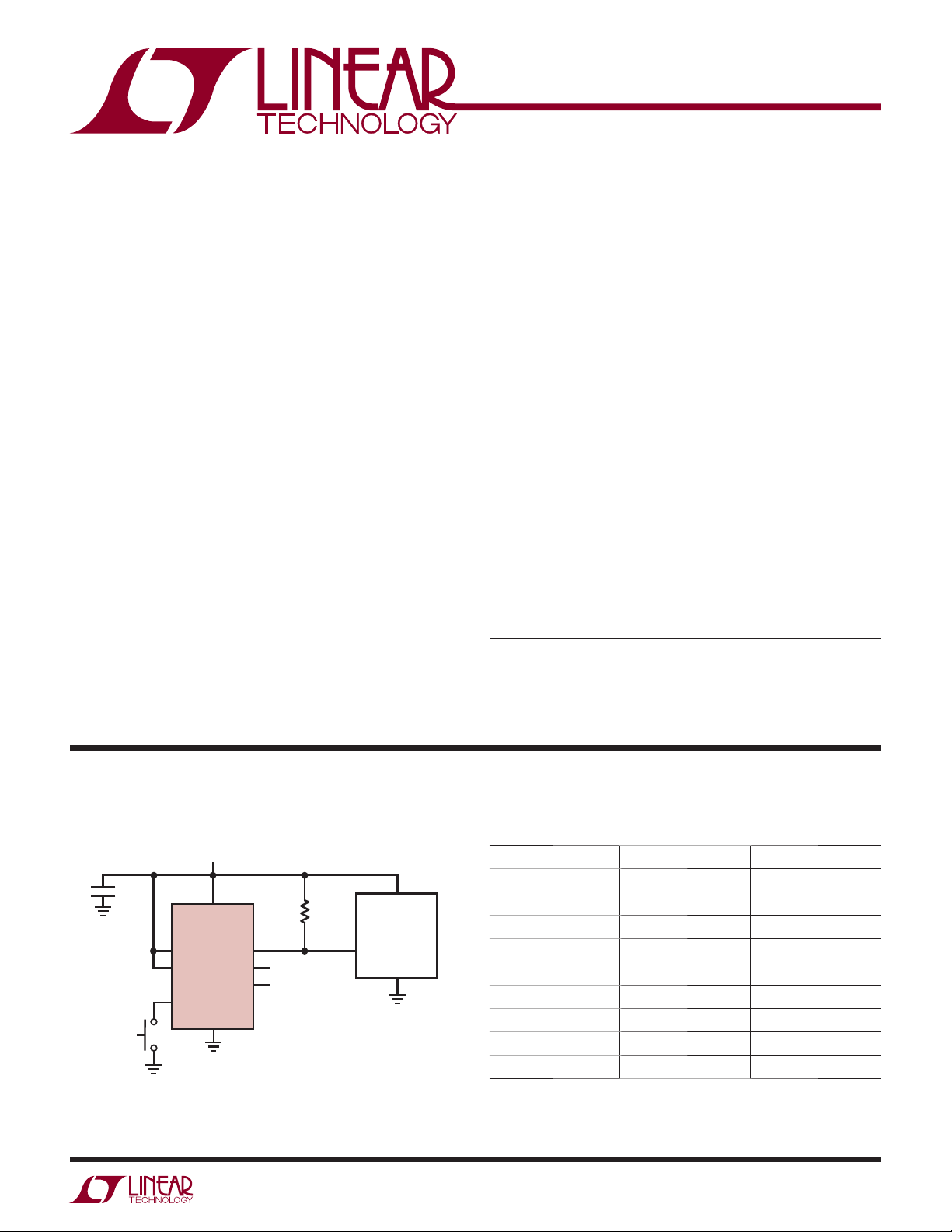
TYPICAL APPLICATION
1.8V, –5% Tolerance Supply Monitor
1.8V
0.1μF
V
CC
LTC2916
VM
RT SEL1
MR
RST RESET
= 200ms
t
SEL2
GND
RST
10k
Monitor Selection Table
NOMINAL VOLTAGE SEL1 SEL2
12V V
V
CC
μP
29156 TA01
5V V
3.3V V
2.5V Open V
1.8V Open Open
1.5V Open GND
1.2V GND V
1V GND Open
ADJ (0.5V) GND GND
CC
CC
CC
V
CC
Open
GND
CC
CC
29156fa
1

LTC2915/LTC2916
ABSOLUTE MAXIMUM RATINGS
(Notes 1, 2)
Terminal Voltages
(Note 3) .......................................... –0.3V to 5.7V
V
CC
SEL1, SEL2, TOL, MR, RST .................. –0.3V to 7.5V
VM ......................................................... –0.3V to 15V
RT .............................................–0.3V to (V
+ 0.3)V
CC
Terminal Currents
(Note 3) .......................................................±5mA
V
CC
PIN CONFIGURATION
TOP VIEW
VM 1
SEL1 2
TOL/MR 3
GND 4
TS8 PACKAGE
8-LEAD PLASTIC TSOT-23
TOL FOR LTC2915
MR FOR LTC2916
= 150°C, θJA = 250°C/W
T
JMAX
8 V
CC
7 SEL2
6 RT
5 RST
Operating Temperature Range
LTC2915C/LTC2916C ............................... 0°C to 70°C
LTC2915I/LTC2916I .............................. –40°C to 85°C
LTC2915H/LTC2916H ......................... –40°C to 125°C
Storage Temperature Range ................... –65°C to 150°C
TS8 Lead Temperature (Soldering, 10 sec) ........... 300°C
TOP VIEW
1GND
TOL/MR
2
SEL1
3
VM
4
8-LEAD (3mm s 2mm) PLASTIC DFN
EXPOSED PAD (PIN 9) PCB GND CONNECTION OPTIONAL
DDB PACKAGE
TOL FOR LTC2915
MR FOR LTC2916
= 150°C, θJA = 76°C/W
T
JMAX
8
RST
RT
7
9
SEL2
6
V
5
CC
ORDER INFORMATION
LEAD FREE FINISH TAPE AND REEL PART MARKING* PACKAGE DESCRIPTION TEMPERATURE RANGE
LTC2915CTS8-1#PBF
LTC2915ITS8-1#PBF
LTC2915HTS8-1#PBF
LTC2915CDDB-1#PBF
LTC2915IDDB-1#PBF
LTC2915HDDB-1#PBF
LEAD FREE FINISH TAPE AND REEL PART MARKING* PACKAGE DESCRIPTION TEMPERATURE RANGE
LTC2916CTS8-1#PBF
LTC2916ITS8-1#PBF
LTC2916HTS8-1#PBF
LTC2916CDDB-1#PBF
LTC2916IDDB-1#PBF
LTC2916HDDB-1#PBF
Consult LTC Marketing for parts specifi ed with wider operating temperature ranges. *The temperature grade is identifi ed by a label on the shipping container.
Consult LTC Marketing for information on non-standard lead based fi nish parts.
For more information on lead free part marking, go to:
For more information on tape and reel specifi cations, go to:
LTC2915CTS8-1#TRPBF
LTC2915ITS8-1#TRPBF
LTC2915HTS8-1#TRPBF
LTC2915CDDB-1#TRPBF
LTC2915IDDB-1#TRPBF
LTC2915HDDB-1#TRPBF
LTC2916CTS8-1#TRPBF
LTC2916ITS8-1#TRPBF
LTC2916HTS8-1#TRPBF
LTC2916CDDB-1#TRPBF
LTC2916IDDB-1#TRPBF
LTC2916HDDB-1#TRPBF
LT C V Q
LT C V Q
LT C V Q
LCVR
LCVR
LCVR
LT D C W
LT D C W
LT D C W
LDCX
LDCX
LDCX
http://www.linear.com/leadfree/
http://www.linear.com/tapeandreel/
8-Lead TSOT-23
8-Lead TSOT-23
8-Lead TSOT-23
8-Lead (3mm × 2mm) Plastic DFN
8-Lead (3mm × 2mm) Plastic DFN
8-Lead (3mm × 2mm) Plastic DFN
8-Lead TSOT-23
8-Lead TSOT-23
8-Lead TSOT-23
8-Lead (3mm × 2mm) Plastic DFN
8-Lead (3mm × 2mm) Plastic DFN
8-Lead (3mm × 2mm) Plastic DFN
0°C to 70°C
–40°C to 85°C
–40°C to 125°C
0°C to 70°C
–40°C to 85°C
–40°C to 125°C
0°C to 70°C
–40°C to 85°C
–40°C to 125°C
0°C to 70°C
–40°C to 85°C
–40°C to 125°C
29156fa
2
LTC2915/LTC2916
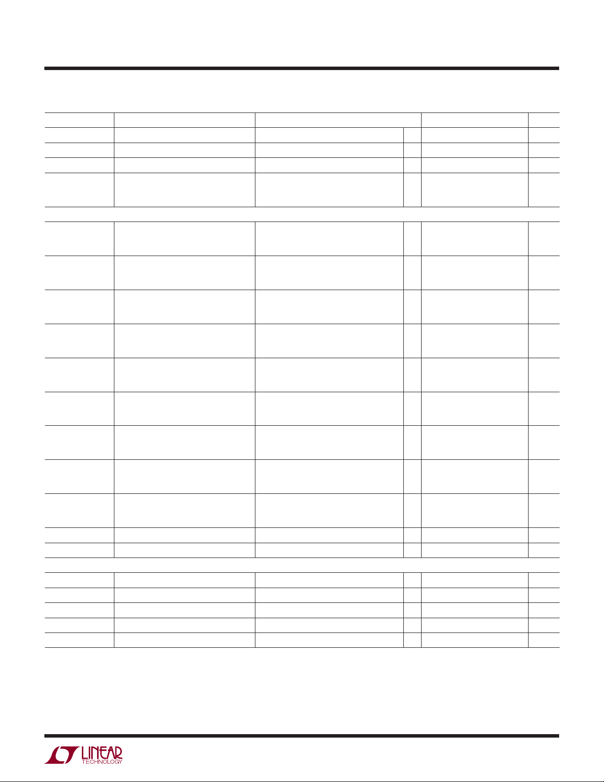
ELECTRICAL CHARACTERISTICS
The l denotes the specifi cations which apply over the full operating
temperature range, otherwise specifi cations are at T
SYMBOL PARAMETER CONDITIONS MIN TYP MAX UNITS
V
CC(MIN)
V
CC(UVLO)
V
CC(SHUNT)
I
CC
Monitor Input (VM)
V
MT120
V
MT50
V
MT33
V
MT25
V
MT18
V
MT15
V
MT12
V
MT10
V
MTADJ
R
VM
I
VM(ADJ)
Three-State Inputs (SEL1, SEL2), (TOL, LTC2915)
V
TPIN,LOW
V
TPIN,HIGH
V
TPIN,Z
I
TPIN,Z
I
TPIN,H/L
Supply Voltage for Guaranteed RST Low RST Driven Low
Supply Undervoltage Lockout
Shunt Regulation Voltage I
VCC Pin Current SEL1, SEL2, TOL, MR = Open
12V, 5% Reset Threshold
12V, 10% Reset Threshold
12V, 15% Reset Threshold
5V, 5% Reset Threshold
5V, 10% Reset Threshold
5V, 15% Reset Threshold
3.3V, 5% Reset Threshold
3.3V, 10% Reset Threshold
3.3V, 15% Reset Threshold
2.5V, 5% Reset Threshold
2.5V, 10% Reset Threshold
2.5V, 15% Reset Threshold
1.8V, 5% Reset Threshold
1.8V, 10% Reset Threshold
1.8V, 15% Reset Threshold
1.5V, 5% Reset Threshold
1.5V, 10% Reset Threshold
1.5V, 15% Reset Threshold
1.2V, 5% Reset Threshold
1.2V, 10% Reset Threshold
1.2V, 15% Reset Threshold
1V, 5% Reset Threshold
1V, 10% Reset Threshold
1V, 15% Reset Threshold
ADJ (0.5V), 5% Reset Threshold
ADJ (0.5V), 10% Reset Threshold
ADJ (0.5V), 15% Reset Threshold
VM Input Impedance (Note 4) Fixed Threshold Modes
ADJ Input Current VM = 0.5V
Low Level Input Voltage
High Level Input Voltage
Pin Voltage when Open I
Allowable Leakage in Open State
Pin Input Current V
= 25°C. VCC = 2.5V, unless otherwise noted. (Note 2)
A
l
0.8 V
l
= 0.5mA
VCC
SEL1, SEL2, TOL = GND (LTC2915)
MR = V
TPIN
(LTC2916)
CC
= 0μA 0.9 V
= 0V, V
TPIN
CC
l
5.7 6.2 7.0 V
l
l
l
11.04
l
10.44
l
9.84
l
4.600
l
4.350
l
4.100
l
3.036
l
2.871
l
2.706
l
2.300
l
2.175
l
2.050
l
1.656
l
1.566
l
1.476
l
1.380
l
1.305
l
1.230
l
1.104
l
1.044
l
0.984
l
0.920
l
0.870
l
0.820
l
460.0
l
435.0
l
410.0
l
0.5 8
l
l
l
1.4 V
l
l
30
45
11.22
10.62
10.02
4.675
4.425
4.175
3.086
2.921
2.756
2.338
2.213
2.088
1.683
1.593
1.503
1.403
1.328
1.253
1.122
1.062
1.002
0.935
0.885
0.835
467.5
442.5
417.5
1.5 V
50
80
11.40
10.80
10.20
4.750
4.500
4.250
3.135
2.970
2.805
2.375
2.250
2.125
1.710
1.620
1.530
1.425
1.350
1.275
1.140
1.080
1.020
0.950
0.900
0.850
475.0
450.0
425.0
±15 nA
0.5 V
±5 μA
±20 μA
μA
μA
mV
mV
mV
MΩ
V
V
V
V
V
V
V
V
V
V
V
V
V
V
V
V
V
V
V
V
V
V
V
V
29156fa
3
LTC2915/LTC2916
ELECTRICAL CHARACTERISTICS
The l denotes the specifi cations which apply over the full operating
temperature range, otherwise specifi cations are at T
SYMBOL PARAMETER CONDITIONS MIN TYP MAX UNITS
Reset Timer Control (RT)
I
RT(UP)
I
RT(DOWN)
I
RT(INT)
V
RT(INT,LH)
Reset Output (RST)
t
RST(INT)
t
RST(EXT)
t
UV
V
OL
I
OH(RST)
Manual Reset Input (LTC2916)
V
IL
V
IH
R
PU
t
PW
RT Pull-Up Current VRT = 0.25V
RT Pull-Down Current VRT = 1.1V
Internal RT VCC Detect Current VRT = V
RT Internal Timer Threshold VRT Rising, Referenced to V
Internal Reset Timeout Period VRT = V
Adjustable Reset Timeout Period CRT = 2.2nF
VM Undervoltage Detect to RST
Asserted
Output Voltage Low RST VCC = 3.3V, I
RST Output Voltage High Leakage RST = V
Input Low Voltage
Input High Voltage
Pull Up Resistance
Pulsewidth
= 25°C. VCC = 2.5V, unless otherwise noted. (Note 2)
A
l
–2 –3 –4 μA
l
234 μA
CC
CC
CC
VM Less Than Reset Threshold
V
by More Than 5%
MTX
= 2.5mA
= 1V, I
= 0.8V, I
CC
RST
= 100μA
RST
RST
= 15μA
V
CC
V
CC
l
l
–100 –160 –300 mV
l
150 200 260 ms
l
16 20 25 ms
l
10 80 150 μs
l
l
l
l
l
l
0.8 • V
l
50 100 150
l
250 ns
18 μA
0.15
0.15
0.05
0.4
0.3
0.2
±1 μA
0.2 • V
CC
CC
kΩ
V
V
V
V
V
Note 1: Stresses beyond those listed under Absolute Maximum Ratings
may cause permanent damage to the device. Exposure to any Absolute
Maximum Rating condition for extended periods may affect device
reliability and lifetime.
Note 2: All currents into pins are positive; all voltages are referenced to
GND unless otherwise noted.
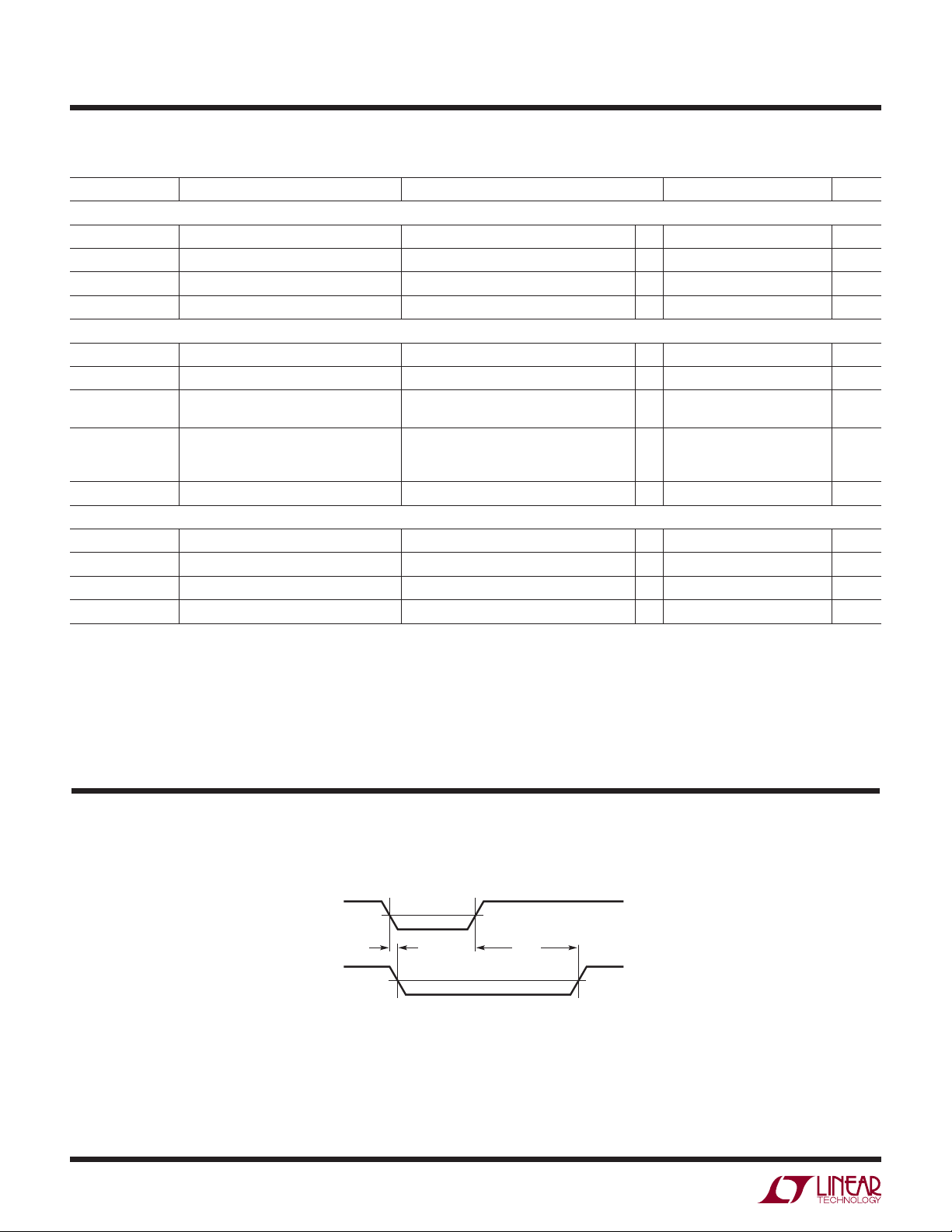
TIMING DIAGRAM
Monitor Input Timing
V
VM
MTx
t
UV
RST
1V
Note 3: VCC maximum pin voltage is limited by input current. Since the
V
pin has an internal 6.2V shunt regulator, a low impedance supply
CC
which exceeds 5.7V may exceed the rated terminal current. Operation
from higher voltage supplies requires a series dropping resistor. See
Applications Information.
Note 4: Input impedance is dependent on the confi guration of the SEL
pins.
t
RST
29156 TD01
4
29156fa

TYPICAL PERFORMANCE CHARACTERISTICS
LTC2915/LTC2916
= 25°C unless otherwise noted.
T
A
Threshold Voltage vs
Temperature
1.5
1.0
(%)
0.5
MTnn
0
V
–0.5
NORMALIZED V
–1.0
–1.5
–50
–25 0
TEMPERATURE (°C)
MT25
50 100 125
25 75
Internal Reset Timeout Period vs
Temperature
250
RT = V
CC
230
RST(INT)
210
V
MTADJ
V
MT120
29156 G01
Quiescent Supply Current vs
Temperature
40
SEL1 = 0V
SEL2 = 2.5V
(μA)
TOL = OPEN
CC
35
VCC = 5.5V
30
25
QUIESCENT SUPPLY CURRENT, I
20
–50
–25 0 25 50
VCC = 2.5V
VCC = 1.5V
TEMPERATURE (°C)
Shunt Regulation Voltage vs
Temperature
6.4
(V)
CC(SHUNT)
6.3
ICC = 5mA
ICC = 1mA
75 100 125
29156 G02
Allowable Glitch Duration vs
Magnitude
300
250
200
150
100
50
MAXIMUM ALLOWABLE GLITCH DURATION (μs)
0
0.1
GLITCH PERCENTAGE PAST THRESHOLD (%)
RESET OCCURS
ABOVE CURVE
1 10 100
Shunt Regulation Voltage vs
Supply Current
7.0
(V)
6.8
CC(SHUNT)
6.6
29156 G03
190
170
RESET TIMEOUT PERIOD (ms), t
150
–50 –25
25
0
TEMPERATURE (°C)
RST Output Voltage vs V
6
100k PULL-UP TO V
SEL1 = SEL2 = TOL = 0V
5
= 0.5V
V
M
4
3
2
RST VOLTAGE (V)
1
0
0
1234
CC
SUPPLY VOLTAGE, VCC (V)
6.2
SHUNT REGULATION VOLTAGE, V
6.1
50
75
100
125
29156 G04
CC
5
29156 G07
–50
RST Pull-Down Current vs V
6
5
(mA)
RST
4
3
2
1
PULL-DOWN CURRENT, I
0
0
ICC = 100μA
–25 0 25 50
TEMPERATURE (°C)
1234
SUPPLY VOLTAGE, VCC (V)
75 100 125
RST AT 150mV
RST AT 50mV
29156 G05
CC
5
29156 G08
6.4
6.2
SHUNT REGULATION VOLTAGE, V
6.0
0.01
RST VOL vs I
1.0
NO PULL-UP R
V
CC
0.8
0.6
0.4
RST VOLTAGE (V)
0.2
0
0
0.1
SUPPLY CURRENT, ICC (mA)
= 2.5V
2
RST
TA = 25°C
4
I
RST
1
(mA)
TA = 125°C
TA = –40°C
6
10
100
29156 G06
8
10
29156 G09
29156fa
5

LTC2915/LTC2916
PIN FUNCTIONS
(TSOT/DFN)
GND (Pin 4/Pin 1): Device Ground.
MR (Pin 3/Pin 2) (LTC2916 only): Manual Reset Input
(Active Low). A low level on the MR input causes the part
to issue a reset, which is released one reset timeout after
the input goes high. The pin has an internal 100k pull-up
, and thus may interface directly to a momentary
to V
CC
pushbutton. Leave open if unused.
RST (Pin 5/Pin 8): Open Drain RST Output. Asserts low
when VM is below the threshold selected by SEL1, SEL2
and TOL input pins. Held low for an adjustable timeout
after VM input is above threshold.
RT (Pin 6/Pin 7): Reset Timeout Control Pin. Attach an
external Capacitor (C
) to GND to set a reset timeout of
RT
9ms/nF. Floating RT generates a reset timeout of approximately 400μs. Tie RT to V
to generate a reset timeout
CC
of approximately 200ms.
SEL1, SEL2 (Pins 2, 7/Pins 3, 6): Monitor Voltage Select
Three-State Inputs. SEL1 and SEL2 control the nominal
threshold voltage that VM is set to monitor. Connect to V
CC
,
GND or leave unconnected in open state. (See Table 1).
TOL (Pin 3/Pin 2) (LTC2915 only): Three-State Input
for Supply Tolerance Selection (–5%, –10% or –15%).
Controls the tolerance band at which the VM supply is
monitored. Connect to V
, GND, or leave unconnected
CC
in open state. (See Table 2).
(Pin 8/Pin 5): Power Supply Input. Bypass this pin
V
CC
to ground with a 0.1μF ceramic capacitor. A minimum of
1.5V on V
ensures that the part is out of under voltage
CC
lockout and that the voltage thresholds are accurate.
Operates as a direct supply input for voltages up to 5.5V.
Operates as a shunt regulator for supply voltages greater
than 5.7V and should have a resistor between this pin and
the supply to limit V
input current to no greater than
CC
5mA. When used without a current-limiting resistor, pin
voltage must not exceed 5.7V.
VM (Pin 1/Pin 4): Voltage Monitor Input to RST Compara-
tor. SEL1, SEL2 and TOL inputs select the exact threshold
that asserts the RST output.
Exposed Pad (Pin 9, DFN Only): Exposed Pad may be left
open or connected to device ground.
BLOCK DIAGRAM
SEL1 MRSEL2
3 STATE
DECODE
VM
+
0.5V
–
MONITOR
DIVIDER
MATRIX
REFERENCE
DIVIDER
MATRIX
TOL
LTC2916LTC2915
RT
V
CC
DETECT
100k
–
+
INTERNAL
200ms TIMER
ADJUSTABLE
RESET TIMER
V
CC
RESET
DRIVER LOGIC
V
V
CC
CC
6.2V
RST
GND
29156 BD
29156fa
6

APPLICATIONS INFORMATION
LTC2915/LTC2916
Supply Monitoring
The LTC2915/LTC2916 are low voltage single supply
monitors with selectable thresholds. Two three-state inputs
select one of nine internally programmed thresholds. For
the LTC2915, a third three-state input selects the tolerance
at which the supply connected to the VM
pin is monitored
(–5%, –10%, –15%). The tolerance for the LTC2916 is
fi xed at –5%. Threshold accuracy is guaranteed at ±1.5%
over the entire operating temperature range.
The LTC2915/LTC2916 asserts the RST output low when
is below the programmed threshold, and for a reset
VM
timeout (t
) after VM goes above the threshold. The reset
RST
timeout can be confi gured to use an internal timer with no
external components, or an adjusted timer programmed
by placing an external capacitor from RT to ground.
Power-Up
powers the drive circuits for the RST pin. Therefore,
V
CC
as soon as V
reaches 0.8V during power up, the RST
CC
output asserts low.
Until V
reaches the undervoltage lockout threshold
CC
(guaranteed less than 1.5V), RST is held low regardless
of the state of VM.
Once V
and VM
timer is started. After the reset timeout (t
is above the under voltage lockout threshold
CC
is above the programmed threshold, the reset
), the open
RST
drain pull-down releases RST and the external pull-up
resistor pulls high.
Power-Down
On power-down, once VM
drops below the undervoltage lockout, RST asserts
V
CC
drops below its threshold or
logic low.
Monitor Threshold Control
The monitor threshold on the VM
pin is controlled by
the SEL1, SEL2 and TOL three-state pins. The SEL1 and
SEL2 pins select one of nine preset nominal voltages
(including one externally adjustable threshold) as shown
in Table 1.
The SEL1 and SEL2 three-state input pins should be connected to GND, V
or left unconnected during normal
CC
operation. Note that when left unconnected, the maximum
leakage allowable from the pin to either GND or V
CC
is
±5μA.
The tolerance at which the monitored supply is measured
is set by the TOL pin (LTC2915 only), as shown in Table 2.
If desired (e.g. for margining purposes), the TOL pin may
be driven by a three-state buffer. That three-state buffer
must have a V
and VOH which meet the VIL and VIH of
OL
the TOL pin specifi ed in the Electrical Characteristics, and
maintain less than 5μA of leakage in the open state.
Threshold Accuracy
The trip threshold for VM is selected by confi guring the
three-state input pins. When using the adjustable input, an
external resistive divider sets the trip threshold, allowing
the user complete control over the trip point. Selection of
this trip voltage is crucial to the reliability of the system.
Table 1. Voltage Threshold Settings
NOMINAL VOLTAGE SEL1 SEL2
CC
V
CC
Open
GND
CC
CC
12V V
5V V
3.3V V
2.5V Open V
1.8V Open Open
1.5V* Open GND
1.2V* GND V
1V* GND Open
ADJ* (0.5V) GND GND
*Require a separate supply for V
Table 2. System Voltage Tolerance Settings
TOLERANCE TOL
–5% V
–10% Open
–15% GND
CC
CC
CC
CC
29156fa
7

LTC2915/LTC2916
APPLICATIONS INFORMATION
Any power supply has some tolerance band within which
it is expected to operate (e.g. 5V±10%). It is generally
undesirable that a supervisor issue a reset when the power
supply is inside this tolerance band. Such a “nuisance”
reset reduces reliability by preventing the system from
functioning under normal conditions.
To prevent nuisance resets, the supervisor threshold must
be guaranteed to lie outside the power supply tolerance
band. To ensure that the threshold lies outside the power
supply tolerance range, the nominal threshold must lie outside that range by the monitor’s accuracy specifi cation.
All 27 of the selectable thresholds have the same relative
threshold accuracy of ±1.5% of the programmed nominal
input voltage (over the full operating temperature range).
Consider the example of monitoring a 5V supply with a 10%
tolerance. The nominal threshold internal to the LTC2915
is 11.5% below the 5V input at 4.425V. With ±1.5% accuracy, the trip threshold range is 4.425V±75mV over
temperature (i.e. 10% to 13% below 5.0V). The monitored
system must thus operate reliably down to 4.35V or 13%
below 5.0V over temperature.
Glitch Immunity
The above discussion is concerned only with the DC
value of the monitored supply. Real supplies also have
relatively high-frequency variation, from sources such as
load transients, noise, and pickup. These variations should
not be considered by the monitor in determining whether
a supply voltage is valid or not. The variations may cause
spurious outputs at RST, particularly if the supply voltage
is near its trip threshold.
Two techniques are used to combat spurious reset without
sacrifi cing threshold accuracy. First, the timeout period
helps prevent high-frequency variation whose frequency
is above 1/ t
from appearing at the RST output.
RST
period, the timer resets and begins again when the supply
next becomes valid.
While the reset timeout is useful at preventing toggling
of the reset output in most cases, it is not effective at
preventing nuisance resets due to short glitches (due to
load transients or other effects) on a valid supply.
To reduce sensitivity to these short glitches, the comparator
has additional anti-glitch circuitry. Any transient at the input
of the comparator needs to be of suffi cient magnitude and
duration t
before it can change the monitor state.
UV
The combination of the reset timeout and anti-glitch circuitry prevents spurious changes in output state without
sacrifi cing threshold accuracy.
Adjustable Input
When the monitor threshold is confi gured as ADJ, the
internal comparator input is connected to the pin without
a resistive divider, and the pin is high-impedance. Thus,
any desired threshold may be chosen by attaching VM
to
a tap point on an external resistive divider between the
monitored supply and ground, as shown in Figure 1.
The reference input of the comparator is controlled by the
tolerance pin. The external resistive divider should make
the voltage at VM = 0.5V when the supply is at nominal
value. The actual threshold of VM accounts for the supply tolerance of ±1.5% guaranteed over the full operating
temperature range. The resulting tolerances are –6.5%,
–11.5%, –16.5% which correspond to 0.468V, 0.443V,
0.418V repectively.
V
MON
R2
VM
R1
–
+
When the voltage at VM
goes below the threshold, the
RST pin asserts low. When the supply recovers past
the threshold, the reset timer starts (assuming it is not
disabled), and RST does not go high until it fi nishes. If
the supply becomes invalid any time during the timeout
8
+
0.5V
–
29156 F01
Figure 1. Setting the Trip Point Using the Adjustable Threshold
29156fa
APPLICATIONS INFORMATION
LTC2915/LTC2916
Typically, the user will pick a value of R1 based on acceptable current draw. Current used by the resistor divider will
be approximately
.
V
⎛
R
105=
⎜
⎝
⎞
⎟
⎠
I
Recommended range of R1 is 1k to 1M. Higher values
of resistance exacerbate the degradation of threshold
accuracy due to leakage currents.
If the nominal value of the supply being monitored is
, then
V
NOM
R2 = R1(2V
NOM
– 1)
Resistor tolerances must be taken into account when
determining the overall accuracy.
Selecting the Reset Timing Capacitor
The reset timeout period can be set to one of two fi xed
internal timers or set with a capacitor in order to accommodate a variety of applications. Connecting a capacitor,
, between the RT pin and ground sets the reset timeout
C
RT
period, t
. The following formula approximates the value
RST
of capacitor needed for a particular timeout:
= t
C
RT
• 110 [pF/ms]
RST
For example, using a standard capacitor value of 2.2nF
would give 20ms delay.
Leaving RT open with no external capacitor generates a
reset timeout of approximately 400μs. Shorting RT to V
CC
generates a reset timeout of approximately 200ms.
RST Output Characteristics
The DC characteristics of the RST pull-down strength
are shown in the Typical Performance Characteristics
section. RST is an open-drain pin and thus requires an
external pull-up resistor to the logic supply. RST may be
pulled above V
, providing the voltage limits of the pin
CC
are observed.
The open-drain of the RST pin allows for wired-OR con-
nection of several LTC2915/LTC2916s.
As noted in the discussion of power up and power down,
the circuits that drive RST are powered by V
fault condition, V
of at least 1V ensures that RST pulls
CC
. During a
CC
low.
Manual Reset (LTC2916 Only)
The LTC2916 includes the MR pin for applications where
a manual reset is desired. MR is internally pulled up, allowing it to interface with a push button with no external
components required. Asserting MR low when RST is high,
initiates a reset, resulting in RST being asserted low for
the set reset timeout.
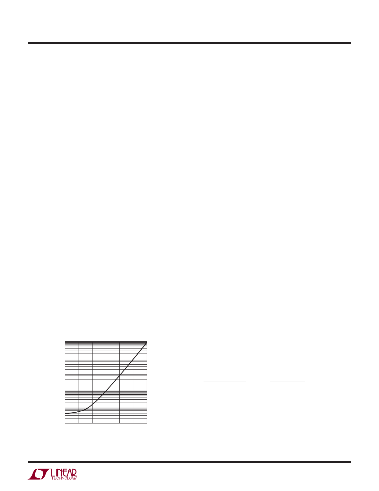
Shunt Regulator
Figure 2 shows the reset timeout period as a function of
the value of the timer capacitor.
10000
1000
(ms)
RST
100
10
1
RESET TIMEOUT PERIOD, t
0.1
0.001
Figure 2. Reset Timeout Period vs RT Capacitance
0.10.01 1 10 100 1000
RT PIN CAPACITANCE, CRT (nF)
29156 F02
The LTC2915 and LTC2916 contain an internal 6.2V shunt
regulator on the V
pin to allow operation from a high
CC
voltage supply. To operate the part from a supply higher
than 5.7V, the V
pin must have a series resistor, RCC, to
CC
the supply. This resistor should be sized according to the
following equation:
VV
SMAX
where V
mA
5
S(MIN)
.−
≤≤
and V
VV
R
CC
are the operating minimum
S(MAX)
−57
250μ
7
A
SMIN() ()
and maximum of the supply.
As an example, consider operation from an automobile
battery which might dip as low as 10V or spike to 60V. We
must then pick a resistance between 10.86k and 12k.
29156fa
9

LTC2915/LTC2916
TYPICAL APPLICATIONS
12V Supply Monitor Powered from 12V, Utilizing
Internal Shunt Regulator with 3.3V Logic Out
12V 3.3V
R
CC
11k
C
BYPASS
V
CC
LTC2915 μP
VM
SEL1 GND
SEL2
TOL
GND RT
RST RST
0.1μF
C
RT
R
10k
PU
V
CC
29156 TA02
5V, –10% Tolerance Supply Monitor with
200ms Internal Reset Timeout
3.3V
5V
3.3V
LTC2915
VM
SEL1
SEL2
TOL
GND RT
V
CC
3.3V
RST
C
BYPASS
0.1μF
R
10k
PU
RST
V
μP
GND
CC
29156 TA03
9V, –15% Tolerance Supply Monitor with 3.3V Logic Out 1V, –15% Tolerance Supply Monitor with 90ms Timeout
R2
866k
R1
51.1k
3.3V
V
LTC2915
VM
SEL1
SEL2
TOL
GND RT
C
BYPASS
0.1μF
CC
RST
C
RT
R
10k
PU
V
CC
μP
RST
GND
29156 TA04
9V
1V
3.3V
LTC2915
VM
SEL1
SEL2
TOL
GND RT
C
BYPASS
0.1μF
V
CC
RST
C
RT
0.01μF
R
10k
PU
V
CC
μP
RST
GND
29156 TA05
1.8V, –5% Supply Monitor with Manual Reset
1.8V
MANUAL RESET
PUSHBUTTON
*OPTIONAL RESISTOR RECOMMENDED TO EXTEND ESD TOLERANCE
10k*
C
BYPASS
0.1μF
V
CC
LTC2916 μP
VM
SEL1 GND
SEL2
MR
GND RT
RST RST
C
RT
R
10k
PU
10
1.5V Supply Monitor with Tolerance Control for Margining,
–5% Operation with –15% Margining
3.3V
V
CC
V
LTC2915
29156 TA07
1.5V
VM
SEL1
SEL2
GND RT
C
BYPASS
0.1μF
CC
RST
C
RT
R
PU
10k
V
CC
μP
RST
I/O
–5%–15%
GND
29156 TA08
29156fa

PACKAGE DESCRIPTION
LTC2915/LTC2916
TS8 Package
8-Lead Plastic TSOT-23
(Reference LTC DWG # 05-08-1637)
0.52
MAX
3.85 MAX
2.62 REF
RECOMMENDED SOLDER PAD LAYOUT
PER IPC CALCULATOR
0.20 BSC
DATUM ‘A’
NOTE:
1. DIMENSIONS ARE IN MILLIMETERS
2. DRAWING NOT TO SCALE
3. DIMENSIONS ARE INCLUSIVE OF PLATING
4. DIMENSIONS ARE EXCLUSIVE OF MOLD FLASH AND METAL BURR
5. MOLD FLASH SHALL NOT EXCEED 0.254mm
6. JEDEC PACKAGE REFERENCE IS MO-193
0.65
REF
0.30 – 0.50 REF
1.22 REF
1.4 MIN
2.80 BSC
0.09 – 0.20
(NOTE 3)
1.50 – 1.75
(NOTE 4)
1.00 MAX
0.65 BSC
0.80 – 0.90
2.90 BSC
(NOTE 4)
PIN ONE ID
1.95 BSC
0.22 – 0.36
8 PLCS (NOTE 3)
0.01 – 0.10
TS8 TSOT-23 0802
DDB Package
8-Lead Plastic DFN (3mm × 2mm)
(Reference LTC DWG # 05-08-1702 Rev B)
0.61 ±0.05
(2 SIDES)
0.70 ±0.05
2.55 ±0.05
1.15 ±0.05
PACKAGE
0.25 ± 0.05
RECOMMENDED SOLDER PAD PITCH AND DIMENSIONS
NOTE:
1. DRAWING CONFORMS TO VERSION (WECD-1) IN JEDEC PACKAGE OUTLINE M0-229
2. DRAWING NOT TO SCALE
3. ALL DIMENSIONS ARE IN MILLIMETERS
4. DIMENSIONS OF EXPOSED PAD ON BOTTOM OF PACKAGE DO NOT INCLUDE
MOLD FLASH. MOLD FLASH, IF PRESENT, SHALL NOT EXCEED 0.15mm ON ANY SIDE
5. EXPOSED PAD SHALL BE SOLDER PLATED
6. SHADED AREA IS ONLY A REFERENCE FOR PIN 1 LOCATION ON THE TOP AND BOTTOM OF PACKAGE
2.20 ±0.05
(2 SIDES)
0.50 BSC
OUTLINE
Information furnished by Linear Technology Corporation is believed to be accurate and reliable.
However, no responsibility is assumed for its use. Linear Technology Corporation makes no representation that the interconnection of its circuits as described herein will not infringe on existing patent rights.
PIN 1 BAR
TOP MARK
(SEE NOTE 6)
0.200 REF
3.00 ±0.10
(2 SIDES)
2.00 ±0.10
(2 SIDES)
0.75 ±0.05
R = 0.05
0 – 0.05
R = 0.115
TYP
0.56 ± 0.05
(2 SIDES)
TYP
0.25 ± 0.05
BOTTOM VIEW—EXPOSED PAD
2.15 ±0.05
(2 SIDES)
0.40 ± 0.10
85
14
0.50 BSC
PIN 1
R = 0.20 OR
0.25 × 45°
CHAMFER
(DDB8) DFN 0905 REV B
29156fa
11

LTC2915/LTC2916
TYPICAL APPLICATION
Dual Supply Monitor (1.8V and 12V) with Manual Reset and 200ms Reset Timeout
1.8V
MANUAL RESET
PUSHBUTTON
C
BYPASS
0.1μF
LTC2916
VM
SEL1
SEL2
MR
GND RT
R
PU
10k
V
CC
RST
1.8V
12V
1.8V
V
CC
LTC2915 μP
VM
SEL1 GND
SEL2
TOL
GND
RST RST
RT
1.8V
V
CC
29156 TA10
RELATED PARTS
PART NUMBER DESCRIPTION COMMENTS
LTC690 5V Supply Monitor, Watchdog Timer and Battery Backup 4.65V Threshold
LTC694-3.3 3.3V Supply Monitor, Watchdog Timer and Battery Backup 2.9V Threshold
LTC1232 5V Supply Monitor, Watchdog Timer and Push-Button Reset 4.37V/4.62V Threshold
LTC1326 Micro Power Precision Triple Supply Monitor 4.725V, 2.363V, 3.118V, 1V Threshold (±0.75%)
LTC1726 Micro Power Triple Supply Monitor for 2.5V/5V, 3.3V and ADJ Adjustable RESET and Watchdog Time-Outs
LTC1727 Micro Power Triple Supply Monitor with Open-Drain Reset Individual Monitor Outputs in MSOP
LTC1728 Micro Power Triple Supply Monitor with Open-Drain Reset 5-Lead SOT-23 Package
LTC1985-1.8 Micro Power Triple Supply Monitor with Push-Pull Reset 5-Lead SOT-23 Package
LTC2900 Programmable Quad Supply Monitor
LTC2901 Programmable Quad Supply Monitor Adjustable RESET and Watchdog Timer, 16-Lead SSOP Package
LTC2902 Programmable Quad Supply Monitor Adjustable RESET and Tolerance, 16-Lead SSOP Package, Margining
LTC2903 Precision Quad Supply Monitor 6-Lead SOT-23 Package, Ultra Low Voltage Reset
LTC2904/LTC2905 3-State Programmable Precision Dual Supply Monitor Adjustable RESET and Tolerance, 8-Lead SOT-23 Package
LTC2906 Precision Dual Supply Monitor 1 Selectable and 1 Adjustable Separate V
LTC2907 Precision Dual Supply Monitor 1 Selectable and 1 Adjustable Separate V
LTC2908 Precision Six Supply Monitor (Four Fixed and 2 Adjustable) 8-Lead SOT-23 and DDB Packages
LTC2909 Precision Triple/Dual Input UV, OV Monitor 2 ADJ Inputs, Monitors Negative Voltages
LTC2910 Octal Positive/Negative Voltage Monitor
LTC2912 Single UV/OV Voltage Monitor, Adjustable UV and OV Trip
Values
LTC2913 Dual UV/OV Voltage Monitor
LTC2914 Qual UV/OV Positive/Negative Voltage Monitor
Adjustable RESET, 10-Lead MSOP and 3mm × 3mm 10-Lead DFN
Pin, RST/RST Outputs
CC
Pin, Adjustable Reset Timer
CC
16-Lead SSOP and 5mm × 3mm DFN Packages
8-Lead TSOT and 3mm × 2mm DFN Packages
10-Lead MOSP and 3mm × 3mm DFN Packages
16-Lead SSOP and 5mm × 3mm DFN Packages
12
Linear Technology Corporation
1630 McCarthy Blvd., Milpitas, CA 95035-7417
(408) 432-1900 ● FAX: (408) 434-0507
●
www.linear.com
29156fa
LT 0108 REV A • PRINTED IN USA
© LINEAR TECHNOLOGY CORPORATION 2007
 Loading...