

Linear Technology LTC2914, LTC2914IGN-2 Datasheet
LTC2914
1
2914fa
Quad UV/OV
Positive/Negative
Voltage Monitor
n
Desktop and Notebook Computers
n
Network Servers
n
Core, I/O Voltage Monitors
n
Monitors Four Voltages Simultaneously
n
Adjustable UV and OV Trip Values
n
Guaranteed Threshold Accuracy: ±1.5% of
Monitored Voltage over Temperature
n
Input Glitch Rejection
n
Monitors up to Two Negative Voltages
n
Buffered 1V Reference Output
n
Adjustable Reset Timeout with Timeout Disable
n
62μA Quiescent Current
n
Open-Drain OV and UV Outputs
n
Guaranteed OV and UV for VCC ≥ 1V
n
Available in 16-Lead SSOP and 16-Lead
(5mm × 3mm) DFN Packages
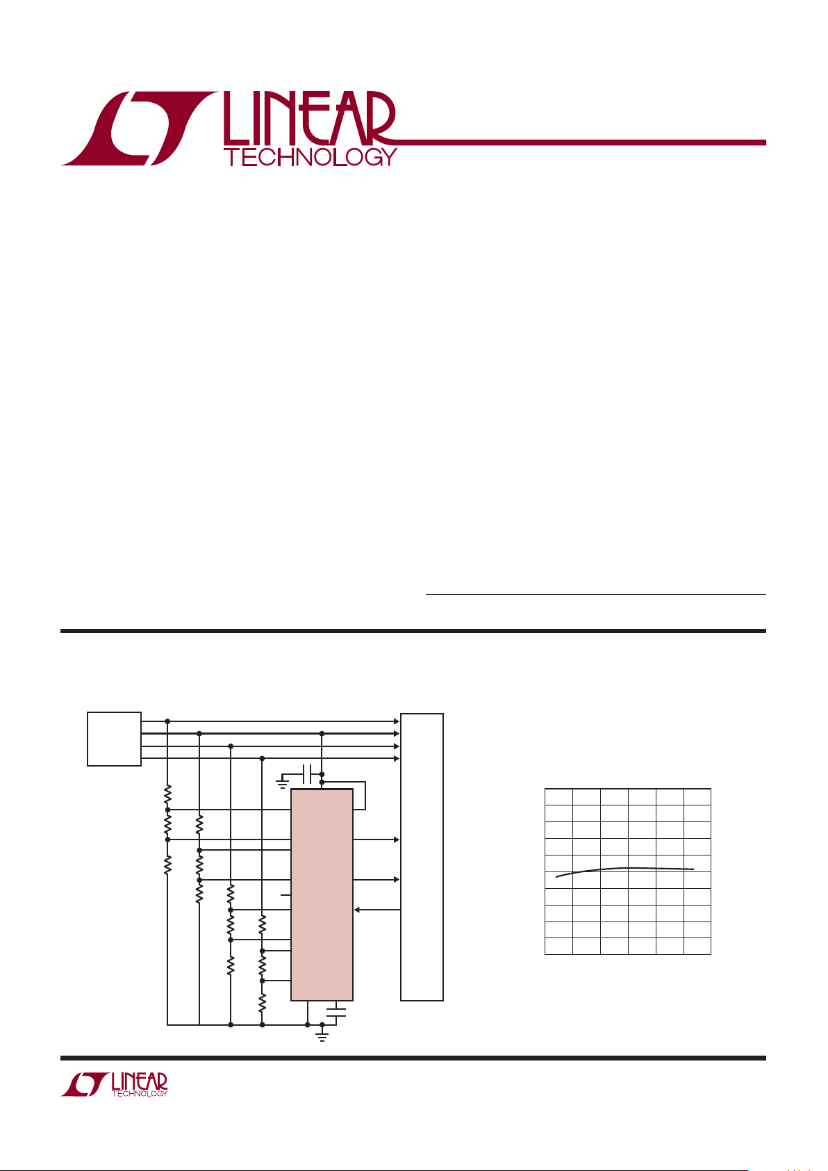
Quad UV/OV Supply Monitor,10% Tolerance, 5V, 3.3V, 2.5V, 1.8V
The LTC®2914 is a quad input voltage monitor intended for
monitoring multiple voltages in a variety of applications.
Dual inputs for each monitored voltage allow monitoring
four separate undervoltage (UV) conditions and four
separate overvoltage (OV) conditions. All monitors share a
common undervoltage output and a common overvoltage
output. The LTC2914-1 has latching capability for the
overvoltage output. The LTC2914-2 has functionality to
disable both the overvoltage and undervoltage outputs.
Polarity selection and a buffered reference allow monitoring
up to two separate negative voltages. A three-state input pin
allows setting the polarity of two inputs without requiring
any external components. Glitch fi ltering ensures reliable
reset operation without false or noisy triggering.
The LTC2914 provides a precise, versatile, space-conscious, micropower solution for voltage monitoring.
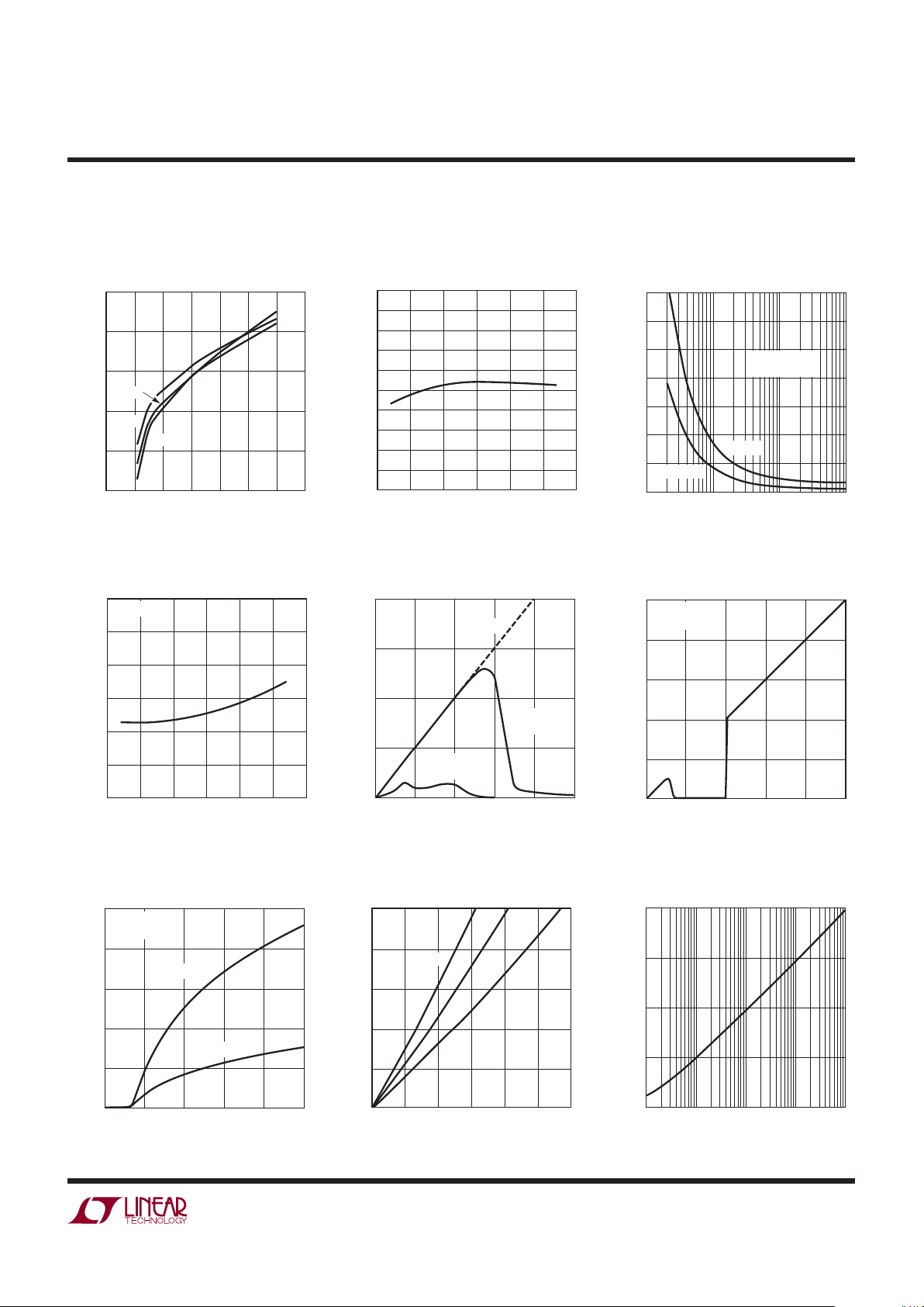
Input Threshold Voltage
vs Temperature
TYPICAL APPLICATION
FEATURES
APPLICATIONS
DESCRIPTION
L, LT, LTC and LTM are registered trademarks of Linear Technology Corporation.
All other trademarks are the property of their respective owners.
VH1
V
CC
LTC2914-1
SYSTEM
2914 TA01a
0.1μF
GND TMR
VL1
VL2
VH2
REF
VL3
VH3
OV
UV
LATCH
SEL
VL4
C
TMR
22nF
TIMEOUT = 200ms
VH4
1k
4.53k
4.53k
12.4k1k
19.6k4.53k
27.4k1k
44.2k
5V
3.3V
2.5V
1.8V
1k
4.53k
P0WER
SUPPLIES
TEMPERATURE (°C)
–50
0.495
THRESHOLD VOLTAGE, V
OUT
(V)
0.497
0.499
0.501
–25
0
25 50
2914 TA01b
75
0.503
0.505
0.496
0.498
0.500
0.502
0.504
100
LTC2914
2
2914fa
Terminal Voltages
V
CC
(Note 3) ............................................. –0.3V to 6V
OV, UV ................................................... –0.3V to 16V
TMR ..........................................–0.3V to (V
CC
+ 0.3V)
VLn, VHn, LATCH, DIS, SEL .................. –0.3V to 7.5V
Terminal Currents
I
VCC
....................................................................10mA
Reference Load Current (I
REF
) ...........................±1mA
I
UV
, IOV ...............................................................10mA
(Notes 1, 2)
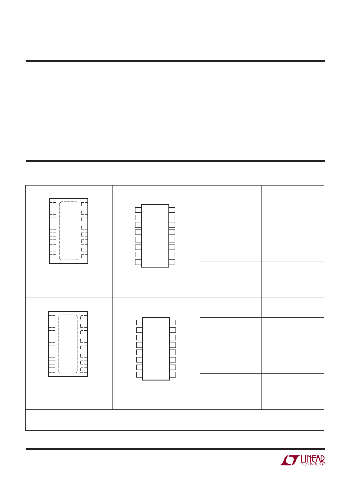
16
15
14
13
12
11
10
9
17
1
2
3
4
5
6
7
8
V
CC
TMR
SEL
LATCH
UV
OV
REF
GND
VH1
VL1
VH2
VL2
VH3
VL3
VH4
VL4
TOP VIEW
DHC PACKAGE
16-LEAD (5mm × 3mm) PLASTIC DFN
T
JMAX
= 150°C, θJA = 43.5°C/W
EXPOSED PAD (PIN 17)
PCB GND CONNECTION OPTIONAL
GN PACKAGE
16-LEAD PLASTIC SSOP
1
2
3
4
5
6
7
8
TOP VIEW
16
15
14
13
12
11
10
9
VH1
VL1
VH2
VL2
VH3
VL3
VH4
VL4
V
CC
TMR
SEL
LATCH
UV
OV
REF
GND
T
JMAX
= 150°C, θJA = 110°C/W
ORDER PART
NUMBER
DHC PART
MARKING*
LTC2914CDHC-1
LTC2914IDHC-1
LTC2914HDHC-1
29141
29141
29141
ORDER PART
NUMBER
GN PART
MARKING
LTC2914CGN-1
LTC2914IGN-1
LTC2914HGN-1
29141
2914I1
2914H1
16
15
14
13
12
11
10
9
17
1
2
3
4
5
6
7
8
V
CC
TMR
SEL
DIS
UV
OV
REF
GND
VH1
VL1
VH2
VL2
VH3
VL3
VH4
VL4
TOP VIEW
DHC PACKAGE
16-LEAD (5mm × 3mm) PLASTIC DFN
T
JMAX
= 150°C, θJA = 43.5°C/W
EXPOSED PAD (PIN 17)
PCB GND CONNECTION OPTIONAL
GN PACKAGE
16-LEAD PLASTIC SSOP
1
2
3
4
5
6
7
8
TOP VIEW
16
15
14
13
12
11
10
9
VH1
VL1
VH2
VL2
VH3
VL3
VH4
VL4
V
CC
TMR
SEL
DIS
UV
OV
REF
GND
T
JMAX
= 150°C, θJA = 110°C/W
ORDER PART
NUMBER
DHC PART
MARKING*
LTC2914CDHC-2
LTC2914IDHC-2
LTC2914HDHC-2
29142
29142
29142
ORDER PART
NUMBER
GN PART
MARKING
LTC2914CGN-2
LTC2914IGN-2
LTC2914HGN-2
29142
2914I2
2914H2
Order Options Tape and Reel: Add #TR
Lead Free: Add #PBF Lead Free Tape and Reel: Add #TRPBF
Lead Free Part Marking: http://www.linear.com/leadfree/
*The temperature grade is identifi ed by a label on the shipping container.
Operating Temperature Range
LTC2914C ................................................0°C to 70°C
LTC2914I.............................................. –40°C to 85°C
LTC2914H .......................................... –40°C to 125°C
Storage Temperature Range ................... –65°C to 150°C
Lead Temperature (Soldering, 10 sec)
SSOP ................................................................ 300°C
ABSOLUTE MAXIMUM RATINGS
PACKAGE/ORDER INFORMATION
LTC2914
3
2914fa
The l denotes the specifi cations which apply over the full operating
temperature range, otherwise specifi cations are at T
A
= 25°C. VCC = 3.3V, VLn = 0.45V, VHn = 0.55V, LATCH = VCC, SEL = VCC,
DIS = Open unless otherwise noted. (Note 2)
SYMBOL PARAMETER CONDITIONS MIN TYP MAX UNITS
V
SHUNT
VCC Shunt Regulator Voltage ICC = 5mA
l
6.2 6.6 6.9 V
–40ºC < T
A
< 125ºC
l
6.2 6.6 7.0 V
ΔV
SHUNT
VCC Shunt Regulator Load Regulation ICC = 2mA to 10mA
l
200 300 mV
V
CC
Supply Voltage (Note 3)
l
2.3 V
SHUNT
V
V
CCR(MIN)
Minimum VCC Output Valid DIS = 0V
l
1V
V
CC(UVLO)
Supply Undervoltage Lockout VCC Rising, DIS = 0V
l
1.9 2 2.1 V
ΔV
CC(UVHYST)
Supply Undervoltage Lockout Hysteresis DIS = 0V
l
52550 mV
I
CC
Supply Current VCC = 2.3V to 6V
l
62 100 μA
V
REF
Reference Output Voltage I
VREF
= ±1mA
l
0.985 1 1.015 V
–40ºC < T
A
< 125ºC
l
0.985 1 1.020 V
V
UOT
Undervoltage/Overvoltage Voltage Threshold
l
492 500 508 mV
t
UOD
Undervoltage/Overvoltage Voltage Threshold
to Output Delay
VHn = V
UOT
– 5mV or VLn = V
UOT
+ 5mV
l
50 125 500 μs
I
VHL
VHn, VLn Input Current
l
±15 nA
–40ºC < T
A
< 125ºC
l
±30 nA
t
UOTO
UV/OV Time-Out Period C
TMR
= 1nF
l
6 8.5 12.5 ms
–40ºC < T
A
< 125ºC
l
6 8.5 14 ms
V
LATCH(IH)
OV Latch Clear Input High
l
1.2 V
V
LATCH(IL)
OV Latch Clear Threshold Input Low
l
0.8 V
I
LATCH
LATCH Input Current V
LATCH
> 0.5V
l
±1 μA
V
DIS(IH)
DIS Input High
l
1.2 V
V
DIS(IL)
DIS Input Low
l
0.8 V
I
DIS
DIS Input Current V
DIS
> 0.5V
l
123 μA
I
TMR(UP)
TMR Pull-Up Current V
TMR
= 0V
l
–1.3 –2.1 –2.8 μA
–40ºC < T
A
< 125ºC
l
–1.2 –2.1 –2.8 μA
I
TMR(DOWN)
TMR Pull-Down Current V
TMR
= 1.6V
l
1.3 2.1 2.8 μA
–40ºC < T
A
< 125ºC
l
1.2 2.1 2.8 μA
V
TMR(DIS)
Timer Disable Voltage Referenced to V
CC
l
–180 –270 mV
V
OH
Output Voltage High UV/OV VCC = 2.3V, I
UV/OV
= –1μA
l
1V
V
OL
Output Voltage Low UV/OV VCC = 2.3V, I
UV/OV
= 2.5mA
V
CC
= 1V, IUV = 100μA
l
l
0.1
0.01
0.3
0.15
V
V
Three-State Input SEL
V
IL
Low Level Input Voltage
l
0.4 V
V
IH
High Level Input Voltage
l
1.4 V
V
Z
Pin Voltage when Left in Hi-Z State I
SEL
= ±10μA
l
0.7 0.9 1.1 V
–40ºC < T
A
< 125ºC
l
0.6 0.9 1.2 V
I
SEL
SEL High, Low Input Current
l
±25 μA
I
SEL(MAX)
Maximum SEL Input Current SEL Tied to Either VCC or GND
l
±30 μA
ELECTRICAL CHARACTERISTICS
LTC2914
4
2914fa
Input Threshold Voltage
vs Temperature
Supply Current vs Temperature
VCC Shunt Voltage
vs Temperature
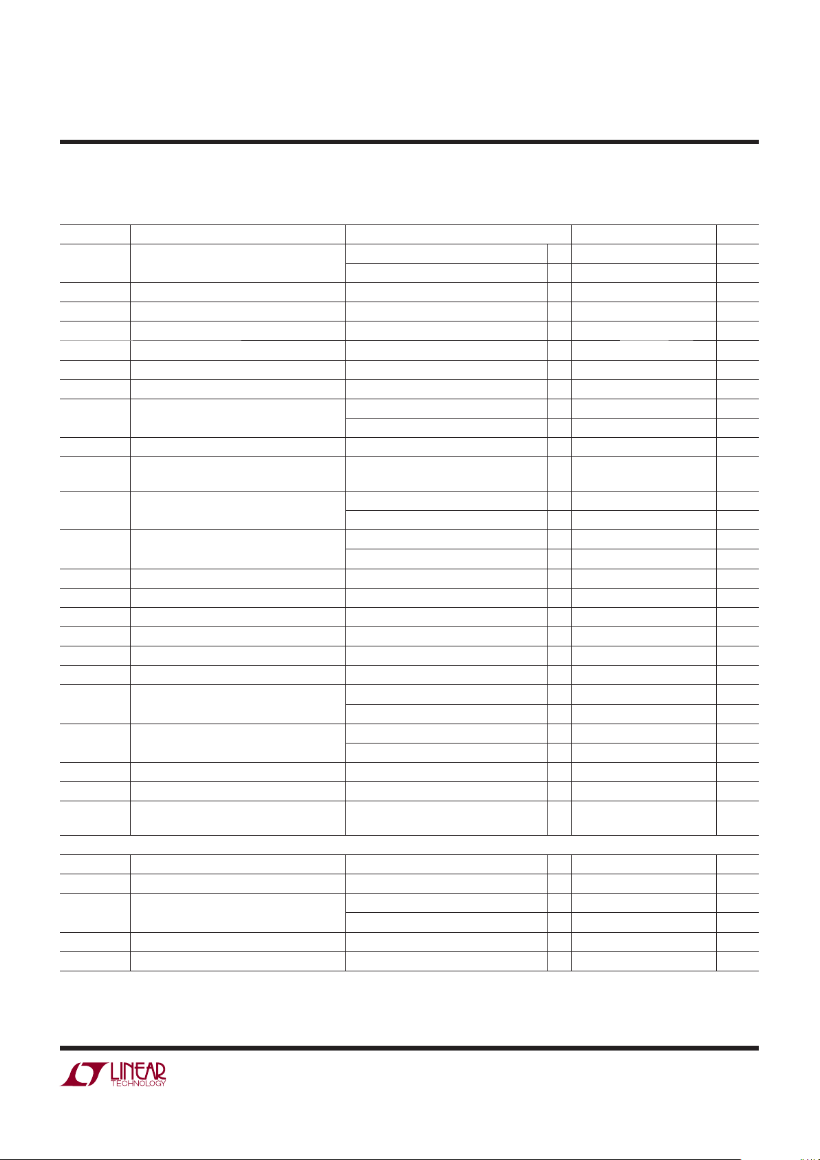
VHn Monitor Timing VLn Monitor Timing
VHn Monitor Timing (TMR Pin Strapped to VCC) VLn Monitor Timing (TMR Pin Strapped to VCC)
NOTE: WHEN AN INPUT IS CONFIGURED AS A NEGATIVE SUPPLY MONITOR, VHn WILL TRIGGER AN OV CONDITION AND VLn WILL TRIGGER A UV CONDITION
Specifi cations are at TA = 25°C, VCC = 3.3V unless otherwise noted.
Note 1: Stresses beyond those listed under Absolute Maximum Ratings
may cause permanent damage to the device. Exposure to any Absolute
Maximum Rating condition for extended periods may affect device
reliability and lifetime.
Note 2: All currents into pins are positive; all voltages are referenced to
GND unless otherwise noted.
Note 3: VCC maximum pin voltage is limited by input current. Since the
V
CC
pin has an internal 6.5V shunt regulator, a low impedance supply that
exceeds 6V may exceed the rated terminal current. Operation from higher
voltage supplies requires a series dropping resistor. See Applications
Information.
ELECTRICAL CHARACTERISTICS
TIIMING DIAGRAMS
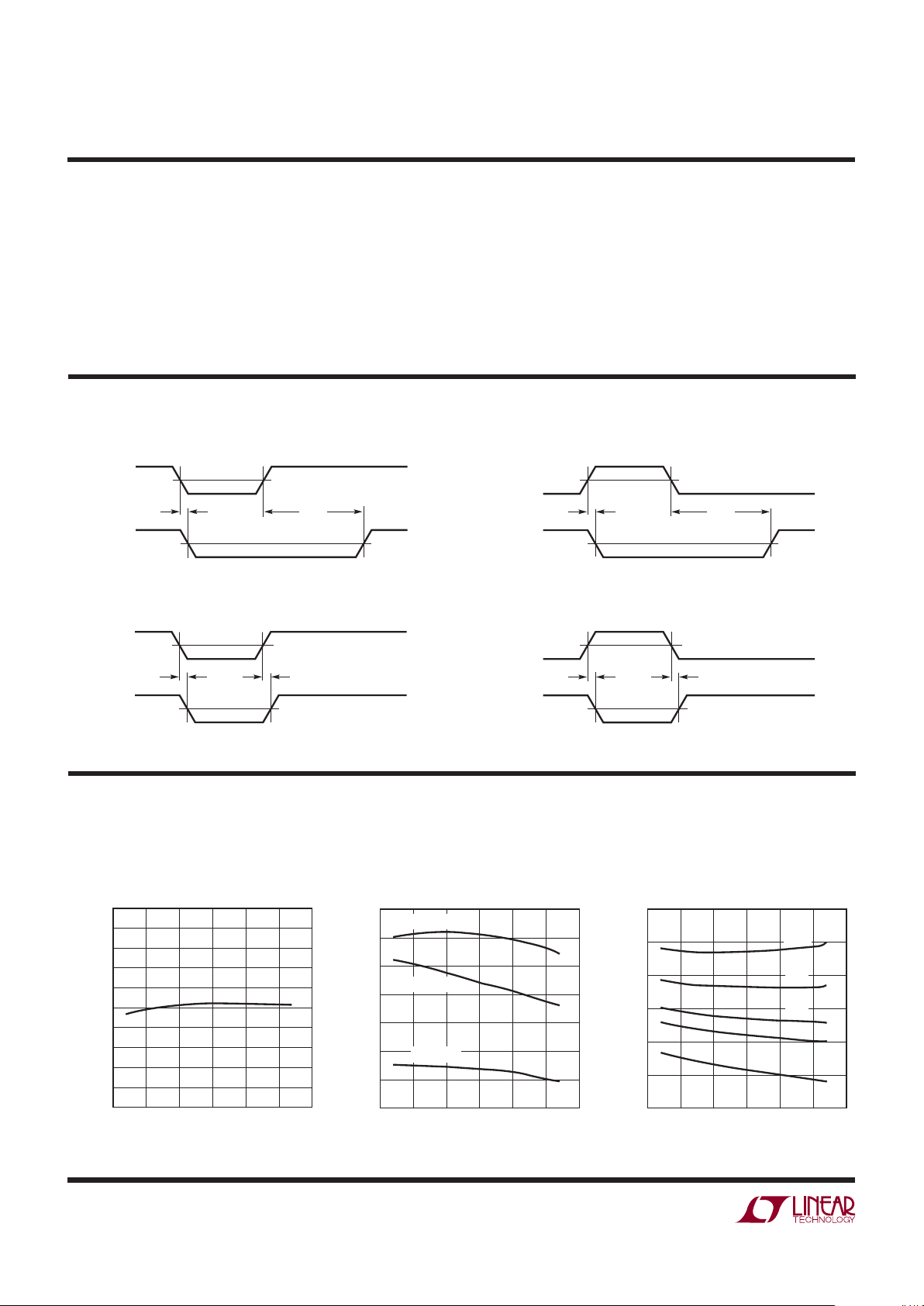
TYPICAL PERFORMANCE CHARACTERISTICS
VHn
UV
V
UOT
1V
t
UOD
t
UOTO
2914 TD01
VLn
OV
V
UOT
1V
t
UOD
t
UOTO
2914 TD02
VHn
UV
V
UOT
1V
t
UOD
t
UOD
2914 TD03
VLn
OV
V
UOT
1V
t
UOD
t
UOD
2914 TD04
TEMPERATURE (°C)
–50
0.495
THRESHOLD VOLTAGE, V
OUT
(V)
0.497
0.499
0.501
–25
0
25 50
2914 G01
75
0.503
0.505
0.496
0.498
0.500
0.502
0.504
100
TEMPERATURE (°C)
–50 50 75–25 25
40
I
CC
(μA)
50
55
45
60
0
2914 G02
100
75
70
65
VCC = 5V
VCC = 3.3V
VCC = 2.3V
TEMPERATURE (°C)
–50
6.2
V
CC
(V)
6.3
6.4
6.5
6.6
6.8
–25
02550
2914 G03
75 100
6.7
200μA
1mA
2mA
5mA
10mA
LTC2914
5
2914fa
VCC Shunt Voltage vs I
CC
Buffered Reference Voltage
vs Temperature
Transient Duration
vs Comparator Overdrive
UV Output Voltage vs V
CC
UV/OV Voltage Output Low
vs Output Sink Current
Reset Timeout Period
vs CapacitanceUV, I
SINK
vs V
CC
Reset Timeout Period
vs Temperature
UV Output Voltage vs V
CC
Specifi cations are at TA = 25°C, VCC = 3.3V unless otherwise noted.
TYPICAL PERFORMANCE CHARACTERISTICS
ICC (mA)
–2 0
6.25
V
CC
(V)
6.45
6.75
2
6
8
2914 G04
6.35
6.65
6.55
4
10
12
25°C
–40°C
85°C
TEMPERATURE (°C)
–50
0.995
REFERENCE VOLTAGE, V
REF
(V)
0.997
0.999
1.001
–25
0
25 50
2914 G05
75
1.003
1.005
0.996
0.998
1.000
1.002
1.004
100
COMPARATOR OVERDRIVE PAST THRESHOLD (%)
0.1
400
TYPICAL TRANSIENT DURATION (μs)
500
600
700
1 10 100
2914 G06
300
200
100
0
VCC = 6V
RESET OCCURS
ABOVE CURVE
VCC = 2.3V
TEMPERATURE (°C)
–50
6
UV/OV TIMEOUT PERIOD, t
UOTO
(ms)
7
8
9
10
12
–25
02550
2914 G07
75 100
11
C
TMR
= 1nF
SUPPLY VOLTAGE, VCC (V)
0
UV VOLTAGE (V)
0.4
0.6
0.8
2914 G08
0.2
0
0.2
0.4
0.6
1.0
0.8
V
CC
UV WITH
10k PULL-UP
UV WITHOUT
10k PULL-UP
SUPPLY VOLTAGE, VCC (V)
0
UV VOLTAGE (V)
3
4
5
4
2914 G09
2
1
0
1
2
3
5
VHn = 0.55V
SEL = V
CC
SUPPLY VOLTAGE, VCC (V)
0
PULL-DOWN CURRENT, I
UV
(mA)
3
4
5
4
2914 G10
2
1
0
1
2
3
5
VHn = 0.45V
SEL = V
CC
UV AT 150mV
UV AT 50mV
I
UV/OV
(mA)
0
0
UV/OV, V
OL
(V)
0.2
0.4
0.6
0.8
1.0
5
10 15 20
2914 G11
25 30
85°C
–40°C
25°C
TMR PIN CAPACITANCE, C
TMR
(nF)
10
UV/OV TIMEOUT PERIOD, t
UOTO
(ms)
100
1000
10000
0.1 10 100 1000
2914 G12
1
1
 Loading...