

LTC2912
Single UV/OV
Voltage Monitor
FEATURES
■
Monitors Single Voltage
■
Adjustable UV and OV Trip Values
■
Guaranteed Threshold Accuracy: ±1.5%
■
Power Supply Glitch Immunity
■
Adjustable Reset Timeout with Timeout Disable
■
29μA Quiescent Current
■
Open-Drain OV and UV Outputs
■
Guaranteed OV and UV for VCC ≥ 1V
■
Available in 8-Lead ThinSOTTM and (3mm × 2mm)
DFN Packages
APPLICATIONS
■
Desktop and Notebook Computers
■
Network Servers
■
Core, I/O Voltage Monitors
DESCRIPTION
The LTC®2912 voltage monitor is designed to detect power
supply undervoltage and overvoltage events. The VL and
VH monitor inputs include fi ltering to reject brief glitches,
thereby ensuring reliable reset operation without false or
noisy triggering. An adjustable timer defi nes the duration of
the overvoltage and under voltage reset outputs which function independently. While the LTC2912 operates directly
from 2.3V to 6V supplies, an internal V
coupled with low supply current demand allows operation
from higher voltages such as 12V, 24V or 48V.
Three output confi gurations are available: the LTC29121 has a latch control for the OV output; the LTC2912-2
has an OV and UV output disable feature for margining
applications; the LTC2912-3 is identical to the LTC2912-1
but with a noninverting, OV output.
The LTC2912 provides a precise, versatile, space-conscious
micropower solution for voltage monitoring.
, LT, LTC and LTM are registered trademarks of Linear Technology Corporation.
ThinSOT is a trademark of Linear Technology Corporation.
All other trademarks are the property of their respective owners.
shunt regulator
CC
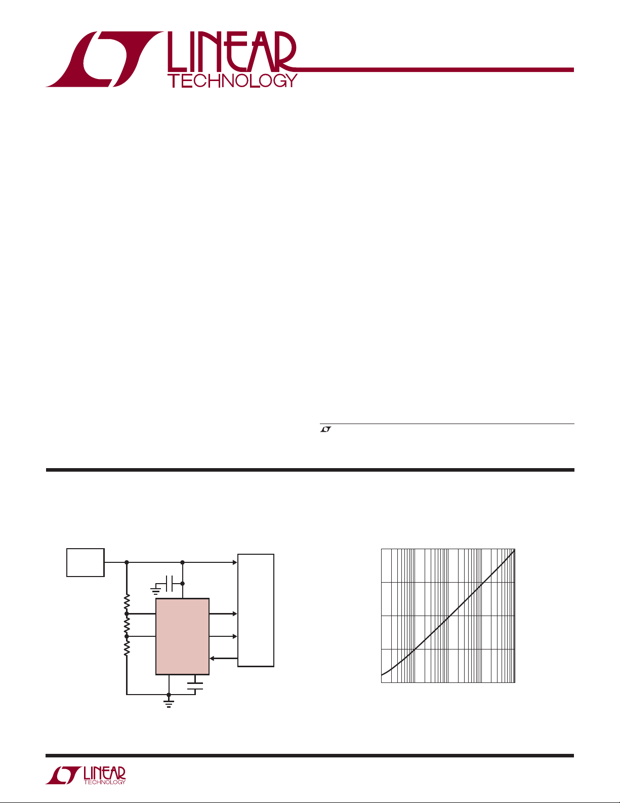
TYPICAL APPLICATION
Single OV/UV Supply Monitor, 3.3V ±10% Tolerance Reset Time-Out Period vs Capacitance
POWER
SUPPLY
3.3V
27.4k
1k
4.53k
0.1μF
V
CC
VH
LTC2912-1
VL
LATCH
GND TMR
OV
UV
22nF
SYSTEM
2912 TA01a
TIMEOUT = 200ms
10000
(ms)
1000
UOTO
100
10
UV/OV TIMEOUT PERIOD, t
1
0.1 10 100 1000
1
TMR PIN CAPACITANCE, C
TMR
(nF)
2912 G08
2912fa
1

LTC2912
(
(
(
ABSOLUTE MAXIMUM RATINGS
Terminal Voltages
VCC (Note 3) ............................................. –0.3V to 6V
OV, UV, OV ............................................ –0.3V to 16V
TMR ..........................................–0.3V to (VCC + 0.3V)
VH, VL, LATCH, DIS .............................. –0.3V to 7.5V
Terminal Currents
I
I
....................................................................10mA
VCC
, IOV, IOV ........................................................10mA
UV
(Note 1)
Operating Temperature Range
LTC2912C ................................................ 0°C to 70°C
LTC2912I.............................................. –40°C to 85°C
LTC2912H .......................................... –40°C to 125°C
Storage Temperature Range
TSOT .................................................. –65°C to 125°C
DFN .................................................... –65°C to 150°C
Lead Temperature (Soldering, 10 sec)
TSOT ................................................................. 300°C
PACKAGE/ORDER INFORMATION
TOP VIEW
TOP VIEW
LATCH 1
UV 2
OV 3
GND 4
TS8 PACKAGE
8-LEAD PLASTIC TSOT-23
T
= 150°C, θJA = 195°C/W
JMAX
8 V
7 VH
6 VL
5 TMR
CC
EXPOSED PAD (PIN 9) IS GND, CONNECTION TO PCB OPTIONAL
CC
VH
VL
TMR
3mm × 2mm) PLASTIC DFN
8-LEAD
T
= 150°C, θJA = 76°C/W
JMAX
ORDER PART NUMBER TS8 PART MARKING* ORDER PART NUMBER DDB PART MARKING*
LTC2912CTS8-1
LTC2912ITS8-1
LTC2912HTS8-1
DIS 1
UV 2
OV 3
GND 4
T
JMAX
TOP VIEW
8 V
7 VH
6 VL
5 TMR
TS8 PACKAGE
8-LEAD PLASTIC TSOT-23
= 150°C, θJA = 195°C/W
LTCJW
LTCJW
LTCJW
CC
LTC2912CDDB-1
LTC2912IDDB-1
LTC2912HDDB-1
CC
VH
VL
TMR
3mm × 2mm) PLASTIC DFN
8-LEAD
T
= 150°C, θJA = 76°C/W
EXPOSED PAD (PIN 9) IS GND, CONNECTION TO PCB OPTIONAL
JMAX
ORDER PART NUMBER TS8 PART MARKING* ORDER PART NUMBER DDB PART MARKING*
LTC2912CTS8-2
LTC2912ITS8-2
LTC2912HTS8-2
LATCH 1
GND 4
T
JMAX
TOP VIEW
UV 2
OV 3
TS8 PACKAGE
8-LEAD PLASTIC TSOT-23
= 150°C, θJA = 195°C/W
8 V
7 VH
6 VL
5 TMR
LTCJX
LTCJX
LTCJX
CC
LTC2912CDDB-2
LTC2912IDDB-2
LTC2912HDDB-2
1V
CC
VH
2
VL
3
TMR
4
DDB PACKAGE
3mm × 2mm) PLASTIC DFN
8-LEAD
T
= 150°C, θJA = 76°C/W
EXPOSED PAD (PIN 9) IS GND, CONNECTION TO PCB OPTIONAL
JMAX
ORDER PART NUMBER TS8 PART MARKING* ORDER PART NUMBER DDB PART MARKING*
LTC2912CTS8-3
LTC2912ITS8-3
LTC2912HTS8-3
Order Options
Tape and Reel: Add #TR Lead Free: Add #PBF Lead Free Tape and Reel: Add #TRPBF Lead Free Part Marking: http://www.linear.com/leadfree/
LTCJY
LTCJY
LTCJY
*The temperature grade is identifi ed by a label on the shipping container.
LTC2912CDDB-3
LTC2912IDDB-3
LTC2912HDDB-3
1V
2
9
3
4
DDB PACKAGE
TOP VIEW
1V
2
9
3
4
DDB PACKAGE
TOP VIEW
9
8
LATCH
UV
7
OV
6
GND
5
LCJZ
LCJZ
LCJZ
8
DIS
UV
7
OV
6
GND
5
LCKB
LCKB
LCKB
8
LATCH
UV
7
OV
6
GND
5
LCKC
LCKC
LCKC
2912fa
2
LTC2912
ELECTRICAL CHARACTERISTICS
The ● denotes the specifi cations which apply over the full operating
temperature range, otherwise specifi cations are at TA = 25°C. VCC = 3.3V, VL = 0.45V, VH = 0.55V, LATCH = VCC unless otherwise
noted. (Note 2)
SYMBOL PARAMETER CONDITIONS MIN TYP MAX UNITS
V
SHUNT
ΔV
SHUNT
V
CC
V
CCR(MIN)
V
CC(UVLO)
ΔV
CC(UVHYST)
I
CC
V
UOT
t
UOD
VCC Shunt Regulator Voltage ICC = 5mA
–40°C < T
A
VCC Shunt Regulator Load Regulation ICC = 2mA to 10mA
Supply Voltage (Note 3)
Minimum VCC Output Valid DIS = 0V
Supply Undervoltage Lockout DIS = 0V, VCC Rising
Supply Undervoltage Lockout Hysteresis DIS = 0V
Supply Current VCC = 2.3V to 6V
Undervoltage/Overvoltage Threshold
Undervoltage/Overvoltage Threshold to
VHn = V
UOT
Output Delay
I
VHL
t
UOTO
V
LATCH(VIH)
V
LATCH(VIL)
I
LATCH
I
DIS
V
DIS(VIH)
V
DIS(VIL)
I
TMR(UP)
I
TMR(DOWN)
V
TMR(DIS)
V
OH
V
OL
VH, VL Input Current
–40°C < T
UV/OV Time-Out Period C
–40°C < T
TMR
A
= 1nF
A
OV Latch Clear Input High
OV Latch Clear Input Low
LATCH Input Current V
DIS Input Current V
LATCH
> 0.5V
DIS
> 0.5V
DIS Input High
DIS Input Low
TMR Pull-Up Current V
TMR Pull-Down Current V
= 0V
TMR
–40°C < T
= 1.6V
TMR
–40°C < T
A
A
Timer Disable Voltage Referenced to V
Output Voltage High UV/OV/OV VCC = 2.3V, I
Output Voltage Low UV/OV/OV VCC = 2.3V, I
V
= 1V, IUV = 100μA
CC
Note 1: Stresses beyond those listed under Absolute Maximum Ratings
may cause permanent damage to the device. Exposure to any Absolute
Maximum Rating condition for extended periods may affect device
reliability and lifetime.
Note 2: All currents into pins are positive; all voltages are referenced to
GND unless otherwise noted.
< 125°
– 5mV or VLn = V
UOT
+ 5mV
< 125°
< 125°
< 125°
< 125°
CC
= –1μA
UV/OV
= 2.5mA
UV/OV
Note 3: VCC maximum pin voltage is limited by input current. Since the
V
pin has an internal 6.5V shunt regulator, a low impedance supply that
CC
exceeds 6V may exceed the rated terminal current. Operation from higher
voltage supplies requires a series dropping resistor. See Applications
Information.
●
6.2 6.6 7.2 V
●
6.2 6.6 7.3 V
●
●
2.3 V
●
●
1.9 2 2.1 V
●
52550 mV
●
●
492 500 508 mV
●
50 125 500 μs
●
●
●
6 8.5 12.5 ms
●
6 8.5 14 ms
●
1.2 V
●
●
●
1 2 3.3 μA
●
1.2 V
●
●
–1.3 –2.1 –2.8 μA
●
–1.2 –2.1 –2.8 μA
●
1.3 2.1 2.8 μA
●
1.2 2.1 2.8 μA
●
–180 –270 mV
●
1V
●
●
200 300 mV
SHUNT
1V
29 70 μA
±15 nA
±30 nA
0.8 V
±1 μA
0.8 V
0.10
0.01
0.30
0.15
V
V
V
2912fa
3
LTC2912
)
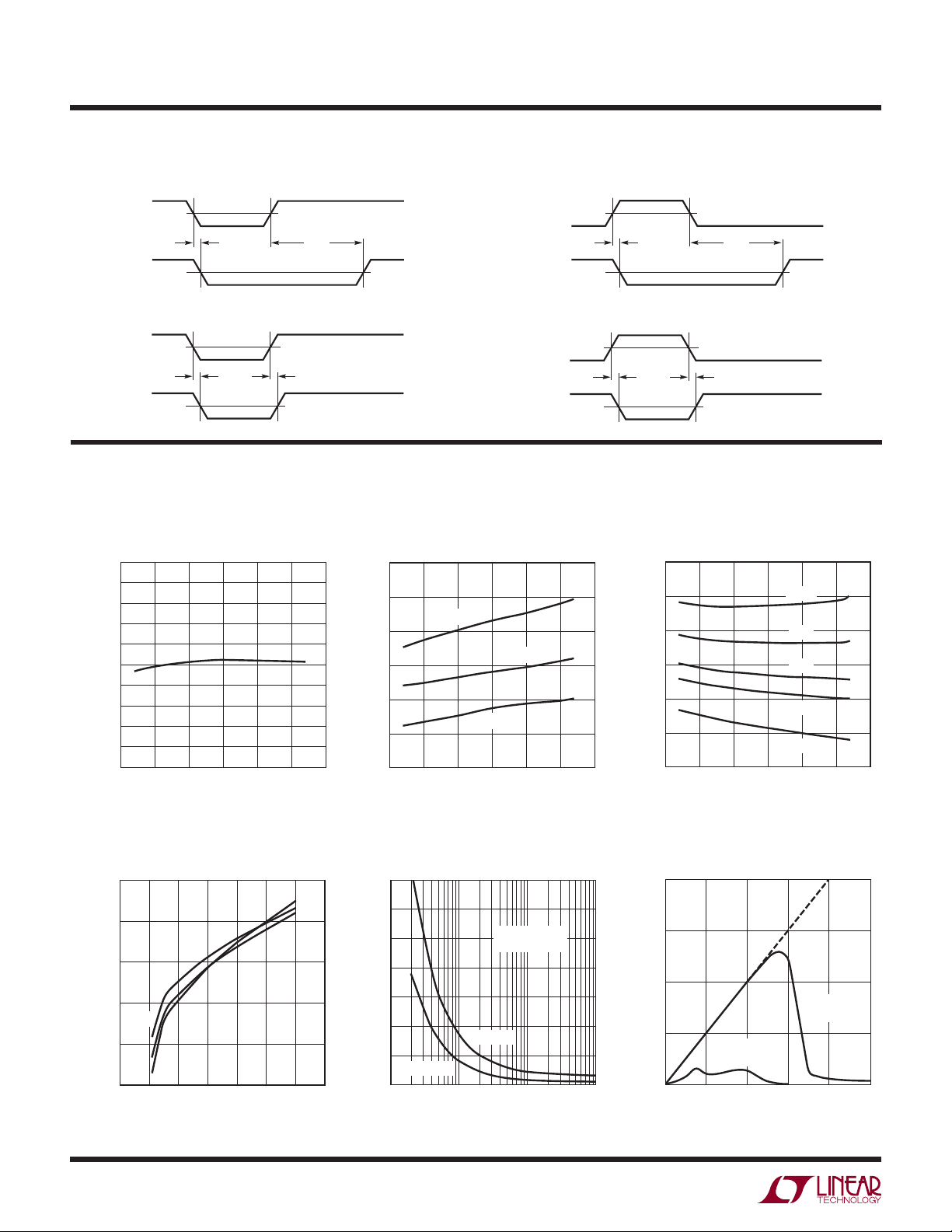
TIMING DIAGRAMS
VH Monitor Timing
V
VH
UOT
t
UOD
UV
1V
VH Monitor Timing (TMR Pin Strapped to V
V
VH
UOT
t
UOD
UV
1V
t
UOD
t
UOTO
2912 TD01
CC
2912 TD03
)
TYPICAL PERFORMANCE CHARACTERISTICS
Input Threshold Voltage
vs Temperature
0.505
0.504
0.503
(V)
UOT
0.502
0.501
0.500
0.499
0.498
0.497
THRESHOLD VOLTAGE, V
0.496
0.495
–50
–25
TEMPERATURE (°C)
0
25 50
75
100
2912 G01
Supply Current vs Temperature
45
40
VCC = 5V
VCC = 3.3V
VCC = 2.3V
–25 0 25 50
TEMPERATURE (°C)
(μA)
CC
I
35
30
25
20
15
–50
VL Monitor Timing
V
VL
UOT
t
UOD
1V
OV
t
UOTO
2912 TD02
VL Monitor Timing (TMR Pin Strapped to VCC)
V
VL
UOT
t
UOD
OV
1V
t
UOD
2912 TD04
VCC Shunt Voltage
vs Temperature
6.8
10mA
5mA
2mA
1mA
200μA
75 100
2912 G02
(V)
CC
V
6.7
6.6
6.5
6.4
6.3
6.2
–50
02550
–25
TEMPERATURE (°C)
75 100
2912 G03
4
VCC Shunt Voltage vs I
6.75
6.65
6.55
(V)
CC
V
6.45
–40°C
6.35
25°C
85°C
6.25
–2 0
2
Typical Transient Duration vs
CC
6
4
I
CC
8
(mA)
10
12
2912 G04
Comparator Overdrive
700
600
500
400
300
200
100
TYPICAL TRANSIENT DURATION (μs)
VCC = 2.3V
50
0.1
COMPARATOR OVERDRIVE PAST THRESHOLD (%
RESET OCCURS
ABOVE CURVE
VCC = 6V
1 10 100
2912 G05
UV Output Voltage vs V
0.8
0.6
0.4
UV VOLTAGE (V)
0.2
0
0
UV WITHOUT
PULL-UP
0.2
SUPPLY VOLTAGE, V
0.4
V
CC
CC
UV WITH
10k PULL-UP
0.6
CC
(V)
0.8
1
2912 G06
2912fa
 Loading...