

Linear Technology LTC2902-2IGN, LTC2902-2CGN, LTC2902-1IGN, LTC2902-1CGN Datasheet
Monitor with Adjustable Reset Timer
FEATURES
■
Simultaneously Monitors Four Supplies
■
16 User Selectable Combinations of 5V, 3.3V, 3V,
2.5V, 1.8V, 1.5V and/or ±Adjustable Voltage
Thresholds
■
Guaranteed Threshold Accuracy: ±1.5% of Monitored
Voltage Over Temperature
■
Selectable Supply Tolerance: 5%, 7.5%,
10%, 12.5% Below Monitored Voltage
■
Low Supply Current: 43µA Typ
■
Adjustable Reset Time
■
RESET Disable Pin for Margining Applications
■
Open-Drain RST Output (LTC2902-1)
■
Push-Pull RST Output (LTC2902-2)
■
Individual Nondelayed Monitor Outputs for Each Supply
■
Power Supply Glitch Immunity
■
Guaranteed RESET for VCC ≥ 1V
U
APPLICATIO S
■
Desktop and Notebook Computers
■
Multivoltage Systems
■
Telecom Equipment
■
Portable Battery-Powered Equipment
■
Network Servers
LTC2902
Programmable Quad Supply
and Supply Tolerance
U
DESCRIPTIO
The LTC®2902 is a programmable supply monitor for systems with up to four supply voltages. One of 16 preset or
adjustable voltage monitor combinations can be selected
using an external resistor divider connected to the program pin. The preset voltage thresholds are digitally programmable to 5%, 7.5%, 10% or 12.5% below the nominal operating voltage, and are accurate to 1.5% over temperature. All four voltage comparator outputs are connected to separate pins for individual supply monitoring.
The reset delay time is adjustable using an external
capacitor. Tight voltage threshold accuracy and glitch
immunity ensure reliable reset operation without false
triggering. The RST output is guaranteed to be in the
correct state for VCC down to 1V and may be disabled
during supply margin testing. The LTC2902-1 features
an open-drain RST output, while the LTC2902-2 has a
push-pull RST output.
The 43µA supply current makes the LTC2902 ideal for power
conscious systems and the part may be configured to
monitor less than four inputs. The LTC2902-1/LTC2902-2
are available in the 16-lead narrow SSOP package.
, LTC and LT are registered trademarks of Linear Technology Corporation.
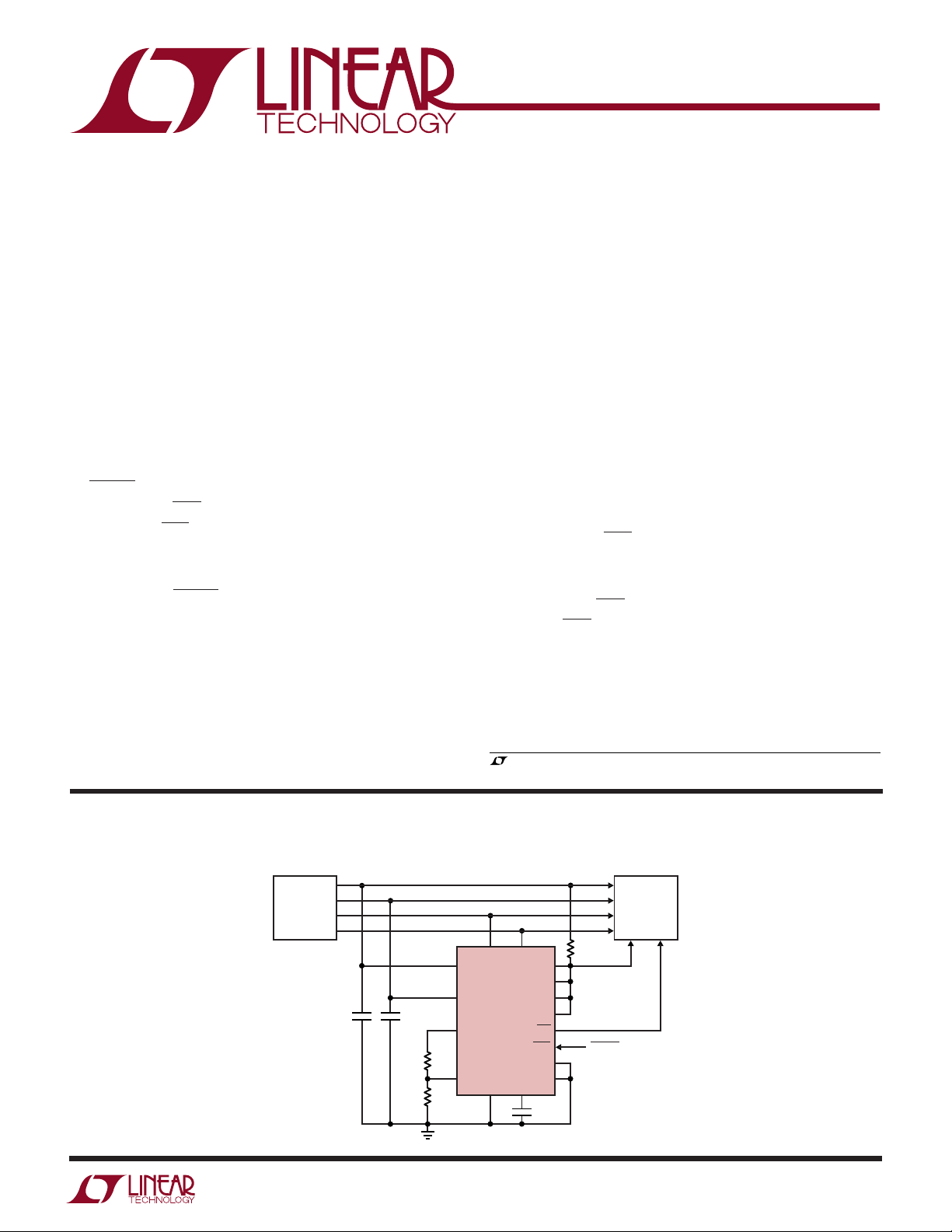
TYPICAL APPLICATIO
Quad Supply Monitor with Adjustable Tolerance (5V, 3.3V, 2.5V, 1.8V)
CONVERTER
DC/DC
U
0.1µF
5V
3.3V
2.5V
1.8V
C1
C2
0.1µF
59k
1%
40.2k
1%
SYSTEM
LOGIC
133
LTC2902-2
GND
10
V4V3
CRT
COMP1
COMP2
COMP3
COMP4
5
4
V1
14
V2
12
V
REF
R1
11
V
R2
PG
RST
RDIS
C
47nF
T0
T1
RT
R3
10k
2
16
1
15
6
8
7
TOLERANCE = 5%
9
2902 TA01
POWER
GOOD
MARGIN
t
RST
= 216ms
2902f
1
LTC2902
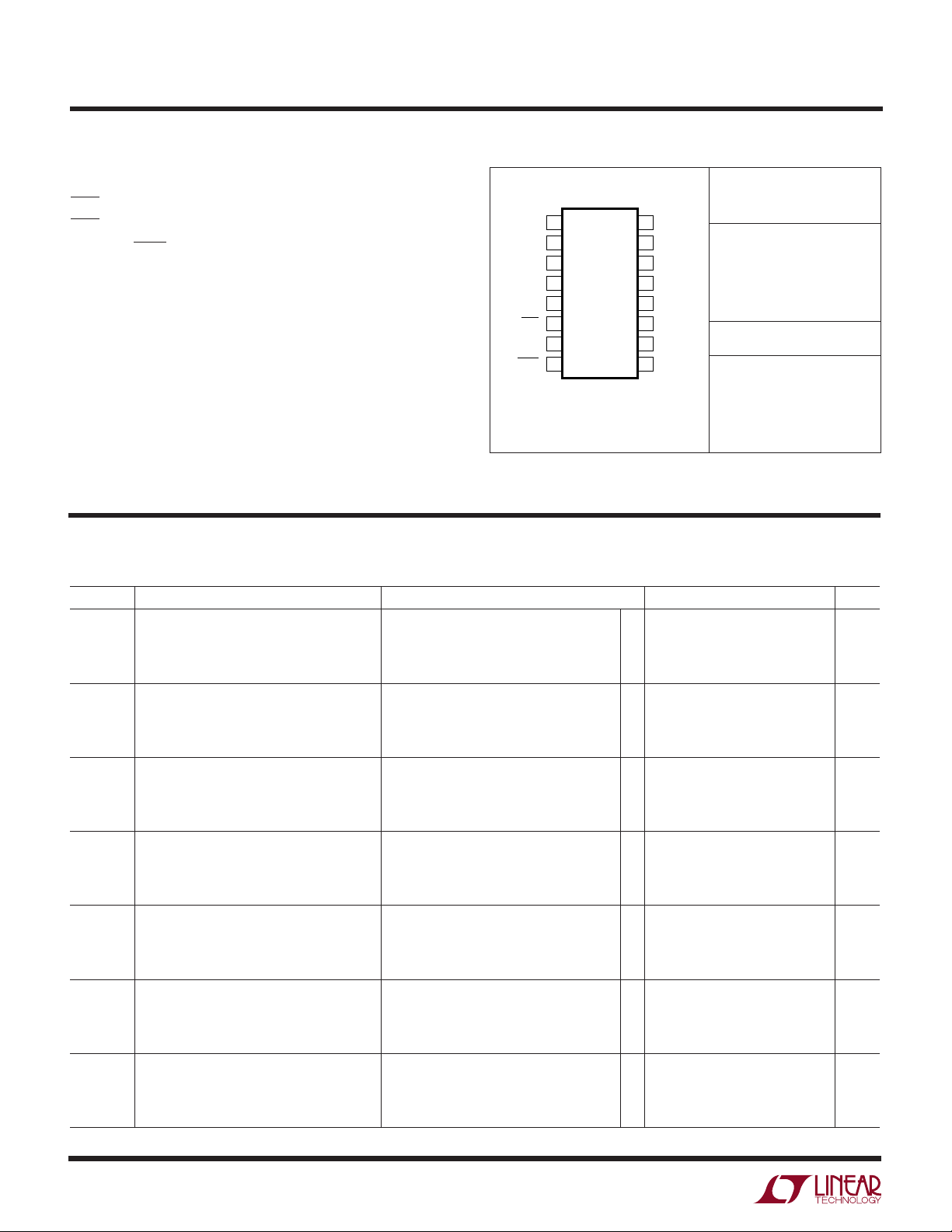
PACKAGE/ORDER I FOR ATIO
UU
W
GN PACKAGE
16-LEAD PLASTIC SSOP
1
2
3
4
5
6
7
8
TOP VIEW
16
15
14
13
12
11
10
9
COMP3
COMP1
V3
V1
CRT
RST
T0
RDIS
COMP2
COMP4
V2
V4
V
REF
V
PG
GND
T1
WWWU
ABSOLUTE AXI U RATI GS
(Notes 1, 2, 3)
V1, V2, V3, V4, VPG..................................... –0.3V to 7V
RST (LTC2902-1)........................................ –0.3V to 7V
RST (LTC2902-2).......................... –0.3V to (V2 + 0.3V)
COMPX, RDIS ............................................. – 0.3V to 7V
T0, T1 .......................................... –0.3V to (VCC + 0.3V)
CRT ............................................. –0.3V to (VCC + 0.3V)
V
............................................. – 0.3V to (VCC + 0.3V)
REF
Reference Load Current (I
V4 Input Current (–ADJ Mode) ............................ –1mA
Operating Temperature Range
LTC2902-1C/LTC2902-2C ....................... 0°C to 70°C
LTC2902-1I/LTC2902-2I .................... –40°C to 85°C
Storage Temperature Range .................. – 65°C to 150°C
Lead Temperature (Soldering, 10 sec)................... 300°C
) ............................ ±1mA
VREF
ORDER PART
NUMBER
LTC2902-1CGN
LTC2902-2CGN
LTC2902-1IGN
LTC2902-2IGN
GN16 PART MARKING
29021
29022
T
= 125°C, θJA = 130°C/W
JMAX
Consult LTC Marketing for parts specified with wider operating temperature ranges.
29021I
29022I
ELECTRICAL CHARACTERISTICS
temperature range, otherwise specifications are at TA = 25°C. VCC = 5V, unless otherwise noted. (Note 3)
SYMBOL PARAMETER CONDITIONS MIN TYP MAX UNITS
V
RT50
V
RT33
V
RT30
V
RT25
V
RT18
V
RT15
V
RTA
2
5V, 5% Reset Threshold V1 Input Threshold ● 4.600 4.675 4.750 V
5V, 7.5% Reset Threshold
5V, 10% Reset Threshold
5V, 12.5% Reset Threshold
3.3V, 5% Reset Threshold V1, V2 Input Threshold ● 3.036 3.086 3.135 V
3.3V, 7.5% Reset Threshold
3.3V, 10% Reset Threshold
3.3V, 12.5% Reset Threshold
3V, 5% Reset Threshold V2 Input Threshold ● 2.760 2.805 2.850 V
3V, 7.5% Reset Threshold
3V, 10% Reset Threshold
3V, 12.5% Reset Threshold
2.5V, 5% Reset Threshold V2, V3 Input Threshold ● 2.300 2.338 2.375 V
2.5V, 7.5% Reset Threshold
2.5V, 10% Reset Threshold
2.5V, 12.5% Reset Threshold
1.8V, 5% Reset Threshold V3, V4 Input Threshold ● 1.656 1.683 1.710 V
1.8V, 7.5% Reset Threshold
1.8V, 10% Reset Threshold
1.8V, 12.5% Reset Threshold
1.5V, 5% Reset Threshold V3, V4 Input Threshold ● 1.380 1.403 1.425 V
1.5V, 7.5% Reset Threshold
1.5V, 10% Reset Threshold
1.5V, 12.5% Reset Threshold
ADJ, 5% Reset Threshold V3, V4 Input Threshold ● 0.492 0.500 0.508 V
ADJ, 7.5% Reset Threshold
ADJ, 10% Reset Threshold
ADJ, 12.5% Reset Threshold
The ● denotes the specifications which apply over the full operating
● 4.475 4.550 4.625 V
● 4.350 4.425 4.500 V
● 4.225 4.300 4.375 V
● 2.954 3.003 3.053 V
● 2.871 2.921 2.970 V
● 2.789 2.838 2.888 V
● 2.685 2.730 2.775 V
● 2.610 2.655 2.700 V
● 2.535 2.580 2.625 V
● 2.238 2.275 2.313 V
● 2.175 2.213 2.250 V
● 2.113 2.150 2.188 V
● 1.611 1.638 1.665 V
● 1.566 1.593 1.620 V
● 1.521 1.548 1.575 V
● 1.343 1.365 1.388 V
● 1.305 1.328 1.350 V
● 1.268 1.290 1.313 V
● 0.479 0.487 0.494 V
● 0.466 0.473 0.481 V
● 0.453 0.460 0.467 V
2902f
LTC2902
ELECTRICAL CHARACTERISTICS
The ● denotes the specifications which apply over the full operating
temperature range, otherwise specifications are at TA = 25°C. VCC = 5V, unless otherwise noted. (Note 3)
SYMBOL PARAMETER CONDITIONS MIN TYP MAX UNITS
V
RTAN
V
CC
V
CCMINP
V
CCMINC
V
REF
V
PG
I
VPG
I
V1
I
V2
I
V3
I
V4
I
CRT(UP)
I
CRT(DN)
t
RST
t
UV
V
OL
V
OH
V
OH
Digital Inputs T0, T1, RDIS
V
IL
V
IH
I
INTOL
V
IL
V
IH
I
RDIS
Note 1: Absolute Maximum Ratings are those values beyond which the life of
a device may be impaired.
Note 2: All voltage values are with respect to GND.
Note 3: The greater of V1, V2 is the internal supply voltage (V
Note 4: Under static no-fault conditions, V1 will necessarily supply quiescent
current. If at any time V2 is larger than V1, V2 must be capable of supplying
the quiescent current, programming (transient) current and reference load
current.
–ADJ Reset Threshold V4 Input Threshold ● –18 0 18 mV
Minimum Internal Operating Voltage RST, COMPX in Correct Logic State; ● 1V
VCC Rising Prior to Program
Minimum Required for Programming VCC Rising ● 2.42 V
Minimum Required for Comparators VCC Falling ● 2.32 V
Reference Voltage VCC ≥ 2.3V, I
= ±1mA, C
VREF
≤ 1000pF
REF
T0 Low, T1 Low ● 1.192 1.210 1.228 V
T0 Low, T1 High
● 1.160 1.178 1.195 V
T0 High, T1 Low ● 1.128 1.146 1.163 V
T0 High, T1 High
Programming Voltage Range VCC ≥ V
VPG Input Current VPG = V
CCMINP
REF
V1 Input Current V1 = 5V, I
= 12µA, (Note 4) ● 43 75 µA
VREF
● 1.096 1.113 1.130 V
● 0V
● ±20 nA
REF
V2 Input Current V2 = 3.3V ● 0.8 2 µA
V3 Input Current V3 = 2.5V ● 0.52 1.2 µA
V3 = 0.55V (ADJ Mode) –15 15 nA
V4 Input Current V4 = 1.8V ● 0.34 0.8 µA
V4 = 0.55V (ADJ Mode)
● –15 15 nA
V4 = –0.05V (–ADJ Mode) ● –15 15 nA
CRT Pull-Up Current V
CRT Pull-Down Current V
= 0V ● –1.4 –2 –2.6 µA
CRT
= 1.3V ● 10 20 30 µA
CRT
Reset Time-Out Period CRT = 1500pF ● 579 ms
VX Undervoltage Detect to RST or COMPX VX Less Than Reset Threshold V
RTX
150 µs
by More Than 1%
Output Voltage Low RST, COMPX I
= 2.5mA; V1 = 3V, V2 = 3V; ● 0.15 0.4 V
SINK
V3, V4 = 0V; VPG = 0V
I
= 100µA; V2 = 1V; V1, V3, V4 = 0V ● 0.05 0.3 V
SINK
I
= 100µA; V1 = 1V; V2, V3, V4 = 0V ● 0.05 0.3 V
SINK
Output Voltage High RST, COMPX (Note 5) I
Output Voltage High RST (LTC2902-2) I
= 1µA ● V2 – 1 V
SOURCE
= 200µA ● 0.8 • V2 V
SOURCE
(Note 6)
T0, T1 Low Level Input Voltage VCC = 3.3V to 5.5V ● 0.3V
T0, T1 High Level Input Voltage VCC = 3.3V to 5.5V ● 0.7V
T0, T1 Input Current T0 = 0V, T1 = V
CC
● ±0.1 ±1 µA
CC
CC
RDIS Input Threshold Low VCC = 3.3V to 5.5V ● 0.4 V
RDIS Input Threshold High VCC = 3.3V to 5.5V ● 1.6 V
RDIS Pull-Up Current V
= 0V –10 µA
RDIS
Note 5: The output pins RST and COMPX have internal pull-ups to V2 of
typically 6µA. However, external pull-up resistors may be used when faster
CC
rise times are required or for V
).
Note 6: The push-pull RST output pin on the LTC2902-2 is
to V2.
voltages greater than V2.
OH
actively
pulled up
2902f
V
V
V
3
LTC2902
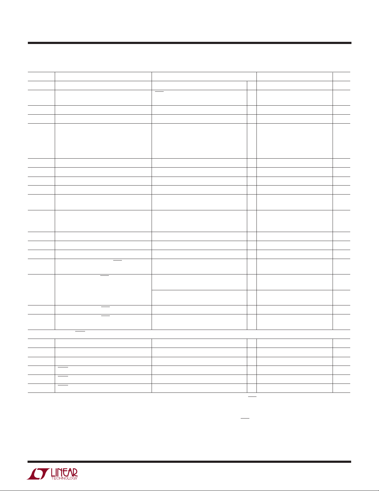
TEST CIRCUITS
V1
V2
V3
V4
LTC2902-1
2902 F01
RST
OR COMPX
I
SOURCE
1µA
V1
V2
V3
V4
LTC2902-1
2902 F02
RST
OR COMPX
I
SINK
2.5mA,
100µA
V1
V2
V3
V4
LTC2902-2
2902 F03
RST
I
SOURCE
200µA
Figure 1. RST, COMPX VOH Test Figure 2. RST, COMPX VOL Test Figure 3. Active Pull-Up RST VOH Test
UWW
TI I G DIAGRA
VX Monitor Timing
V
RTX
t
t
UV
RST
1.5V
2902 TD
RST
COMPX
V
X
UW
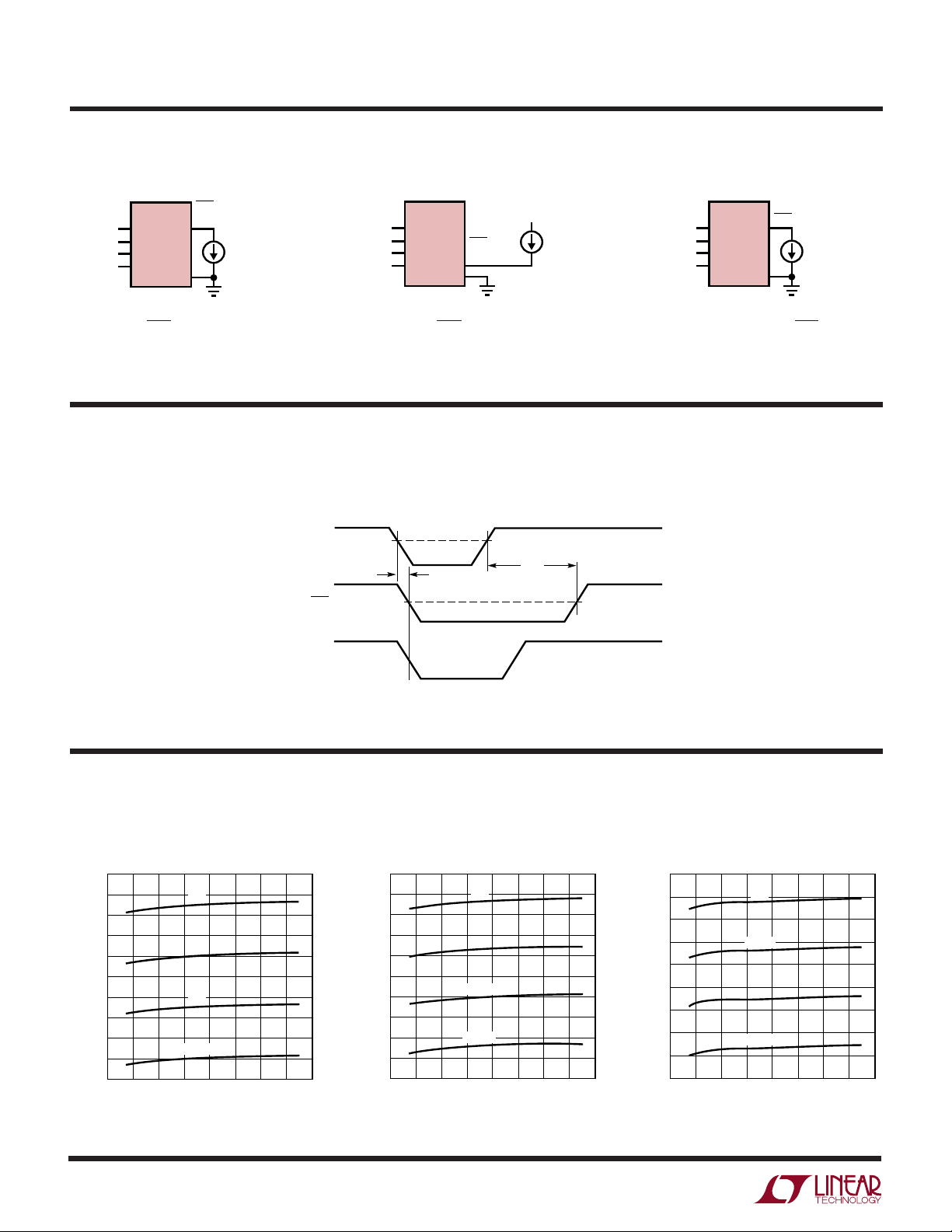
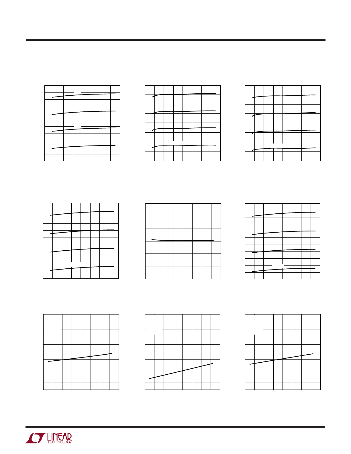
TYPICAL PERFOR A CE CHARACTERISTICS
5V Threshold Voltage
vs Temperature
4.75
4.70
(V)
4.65
RT50
4.60
4.55
4.50
4.45
4.40
4.35
THRESHOLD VOLTAGE, V
4.30
4.25
–60
–20
–40 0
TEMPERATURE (°C)
5%
7.5%
10%
12.5%
20
40
80
60
100
2902 G01
3.3V Threshold Voltage
vs Temperature
3.135
3.100
3.065
(V)
RT33
3.030
2.995
2.960
2.925
2.890
2.855
THRESHOLD VOLTAGE, V
2.820
2.785
–60
–20
–40 0
TEMPERATURE (°C)
5%
7.5%
10%
12.5%
20
60
40
4
80
2902 G02
100
3V Threshold Voltage
vs Temperature
2.850
2.815
(V)
2.780
RT30
2.745
2.710
2.675
2.640
2.605
THRESHOLD VOLTAGE, V
2.570
2.535
–60
–20
–40 0
TEMPERATURE (°C)
5%
7.5%
10%
12.5%
20
40
80
60
100
2902 G03
2902f
UW
TYPICAL PERFOR A CE CHARACTERISTICS
LTC2902
2.5V Threshold Voltage
vs Temperature
2.375
2.350
2.325
(V)
2.300
RT25
2.275
2.250
2.225
2.200
2.175
2.150
THRESHOLD VOLTAGE, V
2.125
2.100
–60
–20
–40 0
TEMPERATURE (°C)
ADJ Threshold Voltage
vs Temperature
0.508
0.503
0.498
(V)
0.493
RTA
0.488
0.483
0.478
0.473
0.468
0.463
THRESHOLD VOLTAGE, V
0.458
0.453
–60
–20
–40 0
TEMPERATURE (°C)
5%
7.5%
10%
12.5%
5%
7.5%
10%
12.5%
1.8V Threshold Voltage
vs Temperature
1.710
1.685
(V)
1.660
RT18
1.635
1.610
1.585
1.560
THRESHOLD VOLTAGE, V
1.535
100
1.510
–60
–40 0
20
40
80
60
2902 G04
5%
7.5%
10%
12.5%
–20
20
TEMPERATURE (°C)
40
100
2902 G05
80
60
1.5V Threshold Voltage
vs Temperature
1.425
1.405
(V)
1.385
RT15
1.365
1.345
1.325
1.305
THRESHOLD VOLTAGE, V
1.285
1.265
–60
–20
–40 0
TEMPERATURE (°C)
5%
7.5%
10%
12.5%
20
40
80
60
100
2902 G06
–ADJ Threshold Voltage
vs Temperature
0.018
0.012
(V)
RTAN
0.006
0
–0.006
–0.012
THRESHOLD VOLTAGE, V
100
–0.018
–60
–40 0
–20
20
TEMPERATURE (°C)
40
100
2902 G08
80
60
20
40
80
60
2902 G07
1.228
1.216
1.204
1.192
1.180
1.168
(V)
REF
1.156
V
1.144
1.132
1.112
1.108
1.096
V
vs Temperature
REF
–60
–20
–40 0
5%
7.5%
10%
12.5%
20
TEMPERATURE (°C)
40
80
60
100
2902 G09
IV1 vs Temperature
100
V1 = 5V
90
V2 = 3.3V
V3 = 2.5V
80
V4 = 1.8V
70
60
50
(µA)
V1
I
40
30
20
10
0
–60
–40 0
–20
20
TEMPERATURE (°C)
40
IV2 vs Temperature
1.5
V1 = 5V
1.4
V2 = 3.3V
V3 = 2.5V
1.3
V4 = 1.8V
1.2
1.1
1.0
(µA)
V2
I
0.9
0.8
0.7
0.6
80
60
100
2902 G10
0.5
–60
–40 0
–20
TEMPERATURE (°C)
80
20
60
40
100
2902 G11
IV3 vs Temperature
1.1
V1 = 5V
1.0
V2 = 3.3V
V3 = 2.5V
0.9
V4 = 1.8V
0.8
0.7
0.6
(µA)
V3
I
0.5
0.4
0.3
0.2
0.1
–60
–40 0
–20
20
TEMPERATURE (°C)
40
80
60
100
2902 G12
2902f
5
 Loading...