


Highly Integrated Quad 16-Bit, SoftSpanTM, Voltage Output DAC
for Industrial and Control Applications
Design Note 431
Mark Thoren
Introduction
Digital-to-analog converters (DACs) are prevalent in
industrial control and automated test applications.
General-purpose automated test equipment often requires many channels of precisely controlled voltages
that span several voltage ranges. The LTC2704 is a
highly integrated 16-bit, 4-channel DAC for high-end
applications. It has a wide range of features designed to
increase performance and simplify design.
Unprecedented Integration
The LTC2704 provides true 16-bit performance over six
software selectable ranges: 0V to 5V, 0V to 10V, –2.5V
to 2.5V, –5V to 5V, –10V to 10V and –2.5V to 7.5V. Four
single-range voltage outputs would normally require
four current-output DACs, two reference amplifi ers and
four output amplifi ers—seven packages if dual amplifi ers are used. Implementing multiple ranges discretely
is prohibitive. Design Note 337 explains the diffi culty in
implementing multiple ranges, including the cos t of precision-matched resistors and the performance limitations
of analog switches. Control is also complicated, requiring
extra digital lines for each DAC and for range control. The
LTC2704 integrates all of these functions into a single
package with no compromises, and all functions are
controlled via an easy-to-use 4-wire SPI bus.
Ease of Use
The LTC2704 provides many features to aid system design. The voltage output and feedback are separated,
allowing external current booster stages to be added
with no loss in accuracy. The C1A, C1B, C1C and C1D
pins allow external frequency compensation capacitors
to be used, either to allow capacitive loads to be directly
dri ven by the LTC2704’s outputs, or to compensate slow
booster stages. The V
pins provide a convenient way
OS
to add an of fset to the output voltage. The gain from the
pin to the output is –0.01, –0.02 or –0.04, depend-
V
OS
ing on the selected range. While this seems like a simple
function to perform externally, implementing it inside
the LTC2704 eliminates concerns about matching the
temperature coeffi cient of the external offset ting resistor
to the internal resistors.
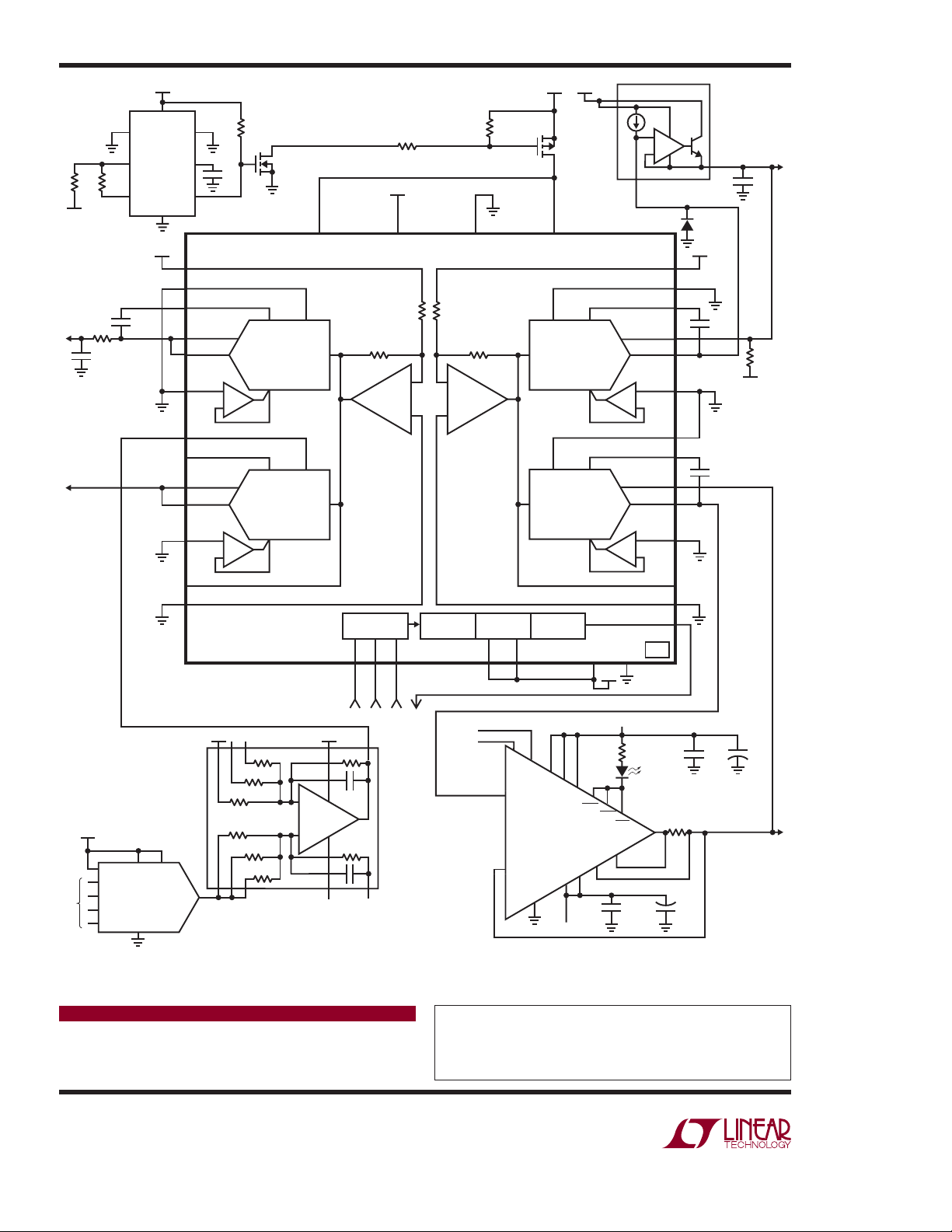
Example Circuits
Figure 1 shows several ways to use the LTC2704’s features. The offset pin of DAC A is driven by an LTC2601
DAC through an LTC1991 amplifi er. This provides ±50mV
of “system offset” adjustment in the ±2.5V and 0V to 5V
ranges, ±100mV of adjustment in the –2.5V to 7.5V, ±5V,
and 0V to 10V ranges and ±200mV of adjustment in the
±10V range. The C1 pin is left open for fast settling. An
LTC2604 quad DAC can be used to drive all four offset
pins, and can share the same SPI bus as the LTC2704.
DAC B drives a 1µF capacitor through a 1Ω resistor, with
2200pF of additional compensation. This is useful for applications where the load has high frequency transients,
such as driving the reference pin of an ADC.
DAC C drives an LT3080 low dropout regulator, providing
up t o 1A of ou tpu t c ur re nt. Th is can be us ed t o p ow er te st
circuitry directly. Global feedback removes the offset of
the regulator, maintaining accuracy at the output.
DAC D is boosted by an LT1970 power op amp, providing
500mA of dr ive current, either sourcing or sinking. Once
again, global feedback preserves DC accuracy.
Conclusion
The LTC2704 provides a highly integrated solution for
generating multiple precision voltages. It saves design
time, board space and cost compared to imple-mentations using separate DACs and amplifi ers.
, LT, LTC and LTM are registered trademarks of Linear Technology Corporation.
SoftSpan is a trademark of Linear Technology Corporation. All other trademarks
are the property of their respective owners.
12/07/431
–15V
309k
+5V
V
CC
SEL
ADJ1
LTC2909-5
ADJ2
TMR
10.7k
REF
RST
GND
+5V
REF1
VOSB
C1B
2200pF
1Ω
1µF
RFBB
OUTB
AGNDB
VOSA
C1A
RFBA
OUTA
1nF
10k
2N7002
DAC B
20k
–15V
+
V
1
–
V
1,8,15,22,31,36
–
10k
AGND V
–
+
–
DAC A
+
+
+15V+15V
V
CONTROL
MTD
2955
+
2
DAC C
LT3080
IN
+
+
–
SET
+5V
REF2
VOSC
C1C
RFBC
OUTC
AGNDC
IN4003
OUT
C2
4.7µF
0.01µF
POSITIVE
RANGES
ONLY
30k
–15V
–
VOSD
C1D
30pF
DAC D
RFBD
OUTD
SPI INTERFACE
+5V
LDAC
CS/LD
SDI
SCK
SDO
±5V
REF
LTC2601
GND
+5V
1.5k
ISRC
SENSE
–
GND
+15V
TSD
OUT
+
0.1MF
AGNDD
+
–
REFM2
REFG2
POR
ERROR
FLAGS
INDICATE
CURRENT
LIMIT AND
THERMAL
SHUTDOWN
SRO
RS, 1Ω
10MF
+
+
10µF0.1µF
±500mA
dn431 F01
AGNDA
+
–
REFM1
REFG1
COMMAND
DECODE
LTC2704
+5V +15V
50k
150k
450k
450k
150k
V
CC
V
OUT
50k
–
+
4pF
–15V
SCK LDACCLRCS/LD RFLAG
SPI INTERFACE
450k
4pF
LT1991
450k
SDI
INPUT
SHIFT REGS
SOURCE
CURRENT
LIMIT
CONTROLS
(0V–5V)
SINK
BUFFERS
500mV
5V
DAC
VC
SRC
+IN
–IN
COMMON
READBACK
SHIFT REGS
VC
SNK
LT1970
V
DD
EN
V
CC
+
V
ISNK
SENSE
–
V
V
EE
–15V
Figure 1. LTC2704 Application Examples
Data Sheet Download
www.linear.com
Linear Technology Corporation
1630 McCarthy Blvd., Milpitas, CA 95035-7417
(408) 432-1900
●
FAX: (408) 434-0507 ● www.linear.com
For applications help,
call (408) 432-1900, Ext. 2602
431f LT/TP 1207 • PRINTED IN THE USA
© LINEAR TECHNOLOGY CORPORATION 2007
 Loading...