

Electrical Specifications Subject to Change
LTC2656
Octal 16-/12-Bit Rail-to-Rail
DACs with 10ppm/°C
Max Reference
FEATURES
n
Precision 10ppm/°C Max Reference
n
Maximum INL Error: ±4LSB at 16 Bits
n
Guaranteed Monotonic over Temperature
n
Selectable Internal or External Reference
n
2.7V to 5.5V Supply Range (LTC2656-L)
n
Integrated Reference Buffers
n
Ultralow Crosstalk Between DACs(<1nV•s)
n
Power-On-Reset to Zero-Scale/Mid-scale
n
Asynchronous LDAC Update Pin
n
Tiny 20-Lead 4mm × 5mm QFN and 20-Lead
Thermally Enhanced TSSOP Packages
APPLICATIONS
n
Mobile Communications
n
Process Control and Industrial Automation
n
Instrumentation
n
Automatic Test Equipment
n
Automotive
DESCRIPTION
The LTC®2656 is a family of octal 16-/12-bit rail-to-rail
DACs with a precision integrated reference. The DACs have
built-in high performance, rail-to-rail, output buffers and
are guaranteed monotonic.The LTC2656-L has a full-scale
output of 2.5V with the integrated 10ppm/°C reference and
operates from a single 2.7V to 5.5V supply. The LTC2656-H
has a full-scale output of 4.096V with the integrated reference and operates from a 4.5V to 5.5V supply. Each DAC can
also operate with an external reference, which sets the DAC
full-scale output to two times the external reference voltage.
These DACs communicate via a SPI/MICROWIRE™ compatible 4-wire serial interface which operates at clock rates
up to 50MHz. The LTC2656 incorporates a power-on reset
circuit that is controlled by the PORSEL pin. If PORSEL
is tied to GND the DACs reset to zero-scale. If PORSEL is
tied to V
L, LT, LTC and LTM are registered trademarks of Linear Technology Corporation.
All other trademarks are the property of their respective owners.
Protected by U.S. Patents, including 5396245, 6891433.
, the DACs reset to mid-scale.
CC
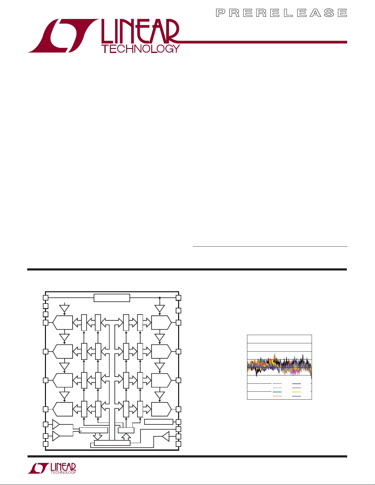
BLOCK DIAGRAM
REFCOMP REFIN/OUT
GND
REFLO
V
OUTA
V
OUTB
V
OUTC
V
OUTD
CS/LD
SCK
LDAC
REF
DAC A
REF
DAC B
REF
DAC C
REF
DAC D
INTERNAL REFERENCE
REGISTER
REGISTER
REGISTER
REGISTER
REGISTER
REGISTER
REGISTER
REGISTER
32-BIT SHIFT REGISTER
DECODECONTROL LOGIC
REGISTER
REGISTER
REGISTER
REGISTER
DAC H V
REGISTER
DAC G V
REGISTER
DAC F V
REGISTER
DAC E V
REGISTER
POWER-ON RESET
REF
REF
REF
REF
V
PORSEL
SDO
SDI
CLR
2656 BD
CC
OUTH
OUTG
OUTF
OUTE
4
3
2
1
0
INL (LSB)
–1
–2
–3
–4
128
INL vs Code
32768
16384
CODE
DACA
DACB
DACC
DACD
49152
DACE
DACF
DACG
DACH
2656 TA01
65535
2656p
1
LTC2656
ABSOLUTE MAXIMUM RATINGS
(Notes 1, 2)
Supply Voltage (VCC) ................................... –0.3V to 6V
CS/LD, SCK, SDI, LDAC, CLR, REFLO .......... –0.3V to 6V
to V
V
OUTA
REFIN/OUT, REFCOMP ...... –0.3V to Min(V
PORSEL, SDO ................... –0.3V to Min(V
................. –0.3V to Min(VCC + 0.3V, 6V)
OUTH
+ 0.3V, 6V)
CC
+ 0.3V, 6V)
CC
Operating Temperature Range
LTC2656C ................................................ 0°C to 70°C
LTC2656I.............................................. –40°C to 85°C
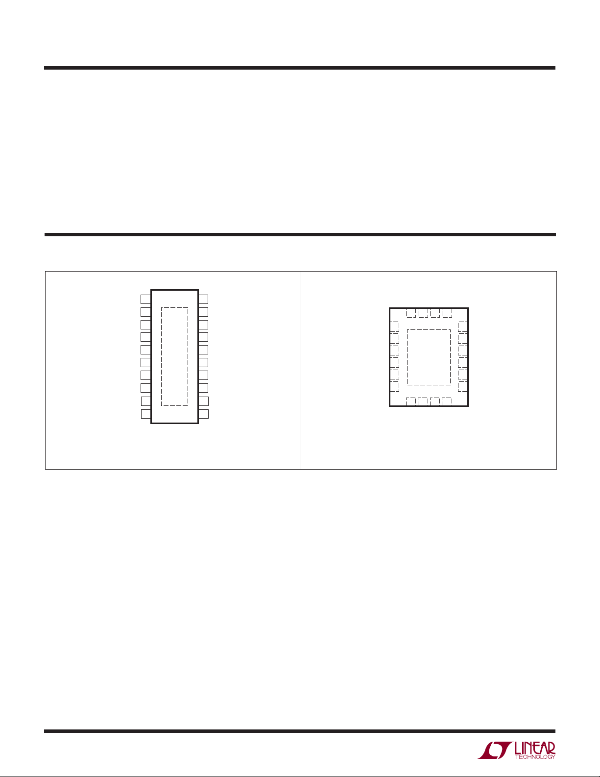
PIN CONFIGURATION
TOP VIEW
1
REFLO
2
V
OUTA
3
V
OUTB
REFCOMP
REFIN/OUT
EXPOSED PAD (PIN 21) IS GND, MUST BE SOLDERED TO PCB
4
5
V
OUTC
V
OUTD
LDAC
CS/LD
SCK
20-LEAD PLASTIC TSSOP
T
= 150°C, θJA = 38°C/W, θJC = 10°C/W
JMAX
6
7
8
9
10
21
FE PACKAGE
20
19
18
17
16
15
14
13
12
11
GND
V
CC
V
OUTH
V
OUTG
V
OUTF
V
OUTE
PORSEL
CLR
SDO
SDI
Maximum Junction Temperature........................... 150°C
Storage Temperature Range .......................–65 to 150°C
Lead Temperature (Soldering, 10 sec)
FE Package .......................................................300°C
TOP VIEW
OUTA
V
20 19 18 17
1
V
OUTB
REFCOMP
REFIN/OUT
EXPOSED PAD (PIN 21) IS GND, MUST BE SOLDERED TO PCB
2
V
3
OUTC
4
V
OUTD
5
6
LDAC
7 8
CS/LD
20-LEAD (4mm s 5mm) PLASTIC QFN
UFD PACKAGE
T
= 150°C, θJA = 43°C/W
JMAX
REFLO
21
9 10
SCK
GND
SDI
CC
V
SDO
16
15
14
13
12
11
V
OUTH
V
OUTG
V
OUTF
V
OUTE
PORSEL
CLR
2
2656p
PRODUCT SELECTOR GUIDE
LTC2656 B C UFD -L 16 #TR PBF
LTC2656
LEAD FREE DESIGNATOR
PBF = Lead Free
TAPE AND REEL
TR = Tape and Reel
RESOLUTION
16 = 16-Bit
12 = 12-Bit
FULL-SCALE VOLTAGE, INTERNAL REFERENCE MODE
L = 2.5V
H = 4.096V
PACKAGE TYPE
UFD = 20-Lead (4mm × 5mm) Plastic QFN
FE = 20-Lead Thermally Enhanced TSSOP
TEMPERATURE GRADE
C = Commercial Temperature Range (0°C to 70°C)
I = Industrial Temperature Range (–40°C to 85°C)
ELECTRICAL GRADE (OPTIONAL)
B = ±4LSB Maximum INL (16-Bit)
PRODUCT PART NUMBER
Consult LTC Marketing for information on non-standard lead based fi nish parts.
For more information on lead free part marking, go to: http://www.linear.com/leadfree/
For more information on tape and reel specifi cations, go to: http://www.linear.com/tapeandreel/
2656p
3
LTC2656
ORDER INFORMATION
LEAD FREE FINISH TAPE AND REEL
LTC2656BCFE-L16#PBF
LTC2656BIFE-L16#PBF
LTC2656BCUFD-L16#PBF
LTC2656BIUFD-L16#PBF
LTC2656BCFE-H16#PBF
LTC2656BIFE-H16#PBF
LTC2656BCUFD-H16#PBF
LTC2656BIUFD-H16#PBF
LTC2656CFE-L12#PBF
LTC2656IFE-L12#PBF
LTC2656CUFD-L12#PBF
LTC2656IUFD-L12#PBF
LTC2656CFE-H12#PBF
LTC2656IFE-H12#PBF
LTC2656CUFD-H12#PBF
L
TC2656IUFD-H12#PBF
Consult LTC Marketing for parts specifi ed with wider operating temperature ranges. *The temperature grade is identifi ed by a label on
the shipping container.Consult LTC Marketing for information on non-standard lead based fi nish parts.
For more information on lead free part marking, go to: http://www.linear.com/leadfree/
For more information on tape and reel specifi cations, go to: http://www.linear.com/tapeandreel/
LTC2656BCFE-L16#TRPBF
LTC2656BIFE-L16#TRPBF
LTC2656BCUFD-L16#TRPBF
LTC2656BIUFD-L16#TRPBF
LTC2656BCFE-H16#TRPBF
LTC2656BIFE-H16#TRPBF
LTC2656BCUFD-H16#TRPBF
LTC2656BIUFD-H16#TRPBF
LTC2656CFE-L12#TRPBF
LTC2656IFE-L12#TRPBF
LTC2656CUFD-L12#TRPBF
LTC2656IUFD-L12#TRPBF
LTC2656CFE-H12#TRPBF
LTC2656IFE-H12#TRPBF
LTC2656CUFD-H12#TRPBF
LTC2656IUFD-H12#TRPBF
PART
MARKING* PACKAGE DESCRIPTION
LTC2656LFE-16
LTC2656LFE-16
56L16
56L16
LTC2656FE-16
LTC2656FE-16
65616
65616
LTC2656LFE-12
LTC2656LFE-12
56L12
56L12
LTC2656FE-12
LTC2656FE-12
65612
65612
20-Lead Thermally Enhanced TSSOP
20-Lead Thermally Enhanced TSSOP
20-Lead (4mm × 5mm) Plastic QFN
20-Lead (4mm × 5mm) Plastic QFN
20-Lead Thermally Enhanced TSSOP
20-Lead Thermally Enhanced TSSOP
20-Lead (4mm × 5mm) Plastic QFN
20-Lead (4mm × 5mm) Plastic QFN
20-Lead Thermally Enhanced TSSOP
20-Lead Thermally Enhanced TSSOP
20-Lead (4mm × 5mm) Plastic QFN
20-Lead (4mm × 5mm) Plastic QFN
20-Lead Thermally Enhanced TSSOP
20-Lead Thermally Enhanced TSSOP
20-Lead (4mm × 5mm) Plastic QFN
20-Lead (4mm × 5mm) Plastic QFN
TEMPERATURE
RANGE MAXIMUM INL
0°C to 70°C
–40°C to 85°C±4±4
0°C to 70°C
–40°C to 85°C±4±4
0°C to 70°C
–40°C to 85°C±4±4
0°C to 70°C
–40°C to 85°C±4±4
0°C to 70°C
–40°C to 85°C±1±1
0°C to 70°C
–40°C to 85°C±1±1
0°C to 70°C
–40°C to 85°C±1±1
0°C to 70°C
–40°C to 85°C±1±1
4
2656p
LTC2656
ELECTRICAL CHARACTERISTICS
The l denotes the specifi cations which apply over the full operating
temperature range, otherwise specifi cations are at T
= 25°C. VCC = 2.7V to 5.5V, V
A
LTC2656B-L16/LTC2656-L12 (internal reference = 1.25V)
SYMBOL PARAMETER CONDITIONS
DC Performance
Resolution
Monotonicity (Note 3)
DNL Differential Nonlinearity (Note 3)
INL Integral Nonlinearity (Note 3) V
Load Regulation V
ZSE Zero-Scale Error
V
OS
Offset Error V
Temperature Coeffi cient 2 2 µV/°C
V
OS
GE Gain Error
Gain Temperature Coeffi cient 1 1 ppm/°C
= 5.5V, V
CC
= 5V ±10%, Internal Reference, Mid-Scale,
CC
–15mA ≤ I
VCC = 3V ±10%, Internal Reference, Mid-Scale,
–7.5mA ≤ I
= 1.25V (Note 4)
REF
REF
OUT
OUT
= 2.5V
≤ 15mA
≤ 7.5mA
unloaded unless otherwise specifi ed.
OUT
LTC2656-12 LTC2656B-16
l
12 16 Bits
l
12 16 Bits
l
l
l
l
l
l
l
±0.1 ±0.5 ±0.3 ±1 LSB
±0.5 ±1 ±2 ±4 LSB
0.04 0.125 0.6 2 LSB/mA
0.06 0.25 1 4 LSB/mA
13 13 mV
±1 ±2 ±1 ±2 mV
±0.02 ±0.1 ±0.02 ±0.1 %FSR
UNITSMIN TYP MAX MIN TYP MAX
SYMBOL PARAMETER CONDITIONS MIN TYP MAX UNITS
V
OUT
DAC Output Span Internal Reference
External Reference = V
EXTREF
0 to 2.5
0 to 2 • V
EXTREF
PSR Power Supply Rejection VCC ±10% –80 dB
R
OUT
DC Output Impedance VCC = 5V ±10%, Internal Reference, Mid-Scale,
–15mA ≤ I
OUT
≤ 15mA
VCC = 3V ±10%, Internal Reference, Mid-Scale,
–7.5mA ≤ I
≤ 7.5mA
OUT
DC Crosstalk (Note 5) Due to Full-Scale Output Change
Due to Load Current Change
Due to Powering Down (per Channel)
I
SC
Short-Circuit Output Current (Note 6) VCC = 5.5V, V
Code: Zero Scale, Forcing Output to V
EXTREF
= 2.75V
CC
Code: Full Scale, Forcing Output to GND
VCC = 2.7V, V
Code: Zero Scale, Forcing Output to V
EXTREF
= 1.35V
CC
Code: Full Scale, Forcing Output to GND
l
l
l
20
l
20
l
10
l
10
0.04 0.15
0.04 0.15
±1.5
±2
±1
60
60
40
40
µV
µV/mA
µV
mA
mA
mA
mA
Reference
Reference Output Voltage 1.248 1.25 1.252 V
Reference Temperature Coeffi cient C-Grade (Note 7)
I-Grade (Note 7)
Reference Line Regulation V
Reference Short-Circuit Current V
REFCOMP Pin Short-Circuit Current V
Reference Load Regulation V
±10% –80 dB
CC
= 5.5V, Forcing Output to GND
CC
= 5.5V, Forcing Output to GND
CC
= 3V ±10% or 5V ±10%, I
CC
= 100µA
OUT
l
l
±2
±2
±10 ppm/°C
ppm/°C
35mA
60 200 µA
40 mV/mA
Sourcing
Reference Output Voltage Noise Density C
REFCOMP
= C
REFIN/OUT
= 0.1µF at f = 1kHz 30 nV/√Hz
V
V
2656p
5
LTC2656
ELECTRICAL CHARACTERISTICS
The l denotes the specifi cations which apply over the full operating
temperature range, otherwise specifi cations are at T
= 25°C. VCC = 2.7V to 5.5V, V
A
LTC2656B-L16/LTC2656-L12 (internal reference = 1.25V)
SYMBOL PARAMETER CONDITIONS MIN TYP MAX UNITS
Reference Input Range External Reference Mode
Reference Input Current
Reference Input Capacitance (Note 9)
Power Supply
V
CC
I
CC
I
SHDN
Digital I/O
V
IH
VIL Digital Input Low Voltage VCC = 4.5V to 5.5V
V
OH
V
OL
I
LK
C
IN
AC Performance
t
S
e
n
Positive Supply Voltage For Specifi ed Performance
Supply Current (Note 8) VCC = 5V, Internal Reference On
V
= 5V, Internal Reference Off
CC
V
= 3V, Internal Reference On
CC
V
= 3V, Internal Reference Off
CC
Supply Current in Shutdown Mode
VCC = 5V
(Note 8)
Digital Input High Voltage VCC = 3.6V to 5.5V
V
= 2.7V to 3.6V
CC
V
= 2.7V to 4.5V
CC
Digital Output High Voltage Load Current = –100µA
Digital Output Low Voltage Load Current = 100µA
Digital Input Leakage VIN = GND to V
CC
Digital Input Capacitance (Note 9)
Settling Time (Note 10) ±0.024% (±1LSB at 12 Bits)
±0.0015% (±1LSB at 16 Bits)
Settling Time for 1LSB Step ±0.024% (±1LSB at 12 Bits)
±0.0015% (±1LSB at 16 Bits)
Voltage Output Slew Rate 1.8 V/µs
Capacitive Load Driving 1000 pF
Glitch Impulse (Note 11) At Mid-Scale Transition, V
= 3V 3 nV•s
CC
DAC-to-DAC Crosstalk (Note 12) Due to Full-Scale Output Change,
C
REFCOMP
= C
REFOUT
= No Load
Multiplying Bandwidth 150 kHz
Output Voltage Noise Density At f = 1kHz
At f = 10kHz
Output Voltage Noise 0.1Hz to 10Hz, Internal Reference
0.1Hz to 200kHz, Internal Reference
unloaded unless otherwise specifi ed.
OUT
l
0.5 VCC/2 V
l
l
l
2.7 5.5 V
l
l
l
l
l
l
2.4
l
2.0
l
l
l
V
– 0.4 V
CC
l
l
l
0.001 1 µA
40 pF
3.1
2.7
3.0
2.6
4.2
8.9
2.2
4.9
2 nV•s
85
80
8
600
4.0
3.5
3.8
3.2
mA
mA
mA
mA
3µA
0.8
0.6
0.4 V
±1 µA
8pF
nV/√Hz
nV/√Hz
µV
P-P
µV
P-P
V
V
V
V
µs
µs
µs
µs
6
2656p
LTC2656
ELECTRICAL CHARACTERISTICS
The l denotes the specifi cations which apply over the full operating
temperature range, otherwise specifi cations are at T
= 25°C. VCC = 4.5V to 5.5V, V
A
LTC2656B-H16/LTC2656-H12 (internal reference = 2.048V)
SYMBOL PARAMETER CONDITIONS
DC Performance
Resolution
Monotonicity (Note 3)
DNL Differential Nonlinearity (Note 3)
INL Integral Nonlinearity (Note 3) V
Load Regulation V
= 5.5V, V
CC
= 5V ±10%, Internal Reference, Mid-Scale,
CC
–15mA ≤ I
ZSE Zero-Scale Error
V
OS
Offset Error V
Temperature Coeffi cient 2 2 µV/°C
V
OS
= 2.048V (Note 4)
REF
GE Gain Error
Gain Temperature Coeffi cient
SYMBOL PARAMETER CONDITIONS MIN TYP MAX UNITS
V
OUT
DAC Output Span Internal Reference
PSR Power Supply Rejection VCC ±10% –80 dB
R
OUT
DC Output Impedance VCC = 5V ±10%, Internal Reference, Midscale,
DC Crosstalk (Note 5) Due to Full-Scale Output Change
I
SC
Short-Circuit Output Current (Note 6) VCC = 5.5V, V
Reference
Reference Output Voltage 2.044 2.048 2.052 V
Reference Temperature Coeffi cient C-Grade (Note 7)
Reference Line Regulation V
Reference Short-Circuit Current VCC = 5.5V, Forcing Output to GND
REFCOMP Pin Short-Circuit Current V
Reference Load Regulation V
Reference Output Voltage Noise Density C
Reference Input Range External Reference Mode
Reference Input Current
Reference Input Capacitance (Note 9)
= 2.5V
REF
≤ 15mA
OUT
External Reference = V
–15mA ≤ I
OUT
EXTREF
≤ 15mA
Due to Load Current Change
Due to Powering Down (per Channel)
= 2.75V
Code: Zero Scale, Forcing Output to V
EXTREF
CC
Code: Full Scale, Forcing Output to GND
I-Grade (Note 7)
±10% –80 dB
CC
= 5.5V, Forcing Output to GND
CC
= 5V ±10%, I
CC
= C
REFCOMP
= 100µA Sourcing 40 mV/mA
OUT
REFIN/OUT
= 0.1µF at f = 1kHz 35 nV/√Hz
unloaded unless otherwise specifi ed.
OUT
LTC2656-12 LTC2656B-16
l
12 16 Bits
l
12 16 Bits
l
l
l
l
l
l
±0.1 ±0.5 ±0.3 ±1 LSB
±0.5 ±1 ±2 ±4 LSB
0.04 0.125 0.6 2 LSB/mA
13 13 mV
±1 ±2 ±1 ±2 mV
±0.02 ±0.1 ±0.02 ±0.1 %FSR
1 1 ppm/°C
0 to 4.096
0 to 2 • V
l
EXTREF
0.04 0.15
±1.5
±2
±1
l
20
l
20
±2
±2
l
l
l
0.5 VCC/2 V
l
l
35mA
60 200 µA
0.001 1 µA
40 pF
UNITSMIN TYP MAX MIN TYP MAX
µV
µV/mA
µV
60
60
mA
mA
±10 ppm/°C
ppm/°C
V
V
2656p
7
LTC2656
ELECTRICAL CHARACTERISTICS
The l denotes the specifi cations which apply over the full operating
temperature range, otherwise specifi cations are at T
= 25°C. VCC = 4.5V to 5.5V, V
A
LTC2656B-H16/LTC2656-H12 (internal reference = 2.048V)
SYMBOL PARAMETER CONDITIONS MIN TYP MAX UNITS
Power Supply
V
CC
I
CC
I
SHDN
Digital I/O
V
IH
V
IL
V
OH
V
OL
I
LK
C
IN
AC Performance
t
S
e
n
Positive Supply Voltage For Specifi ed Performance
Supply Current (Note 8) VCC = 5V, Internal Reference On
V
= 5V, Internal Reference Off
CC
Supply Current in Shutdown Mode
VCC = 5V
(Note 8)
Digital Input High Voltage VCC = 4.5V to 5.5V
Digital Input Low Voltage VCC = 4.5V to 5.5V
Digital Output High Voltage Load Current = –100µA
Digital Output Low Voltage Load Current = 100µA
Digital Input Leakage VIN = GND to V
CC
Digital Input Capacitance (Note 9)
Settling Time (Note 10) ±0.024% (±1LSB at 12 Bits)
±0.0015% (±1LSB at 16 Bits)
Settling Time for 1LSB Step ±0.024% (±1LSB at 12 Bits)
±0.0015% (±1LSB at 16 Bits)
Voltage Output Slew Rate 1.8 V/µs
Capacitive Load Driving 1000 pF
Glitch Impulse (Note 11) At Mid-Scale Transition, V
= 5V 6 nV•s
CC
DAC-to-DAC Crosstalk (Note 12) Due to Full-Scale Output Change,
C
REFCOMP
= C
REFOUT
= No Load
Multiplying Bandwidth 150 kHz
Output Voltage Noise Density At f = 1kHz
At f = 10kHz
Output Voltage Noise 0.1Hz to 10Hz, Internal Reference
0.1Hz to 200kHz, Internal Reference
unloaded unless otherwise specifi ed.
OUT
l
4.5 5.5 V
l
l
l
l
2.4 V
l
l
V
– 0.4 V
CC
l
l
l
3.3
3.0
4.6
7.9
2.0
3.8
3 nV•s
85
80
12
650
4.0
3.7
mA
mA
3µA
0.8 V
0.4 V
±1 µA
8pF
µs
µs
µs
µs
nV/√Hz
nV/√Hz
µV
P-P
µV
P-P
8
2656p
 Loading...