

Page 1
LTC2631
FEATURES
n
Integrated Precision Reference
2.5V Full-Scale 10ppm/°C (LTC2631-L)
4.096V Full-Scale 10ppm/°C (LTC2631-H)
n
Maximum INL Error: 1LSB (LTC2631A-12)
n
Bidirectional Reference: Input or 10ppm/°C Output
n
400kHz I2C™ Interface
n
Nine Selectable Addresses (LTC2631-Z)
n
Low Noise (0.7mV
n
Guaranteed Monotonic Over Temperature
n
2.7V to 5.5V Supply Range (LTC2631-L)
n
Low Power Operation: 180µA at 3V
n
Power Down to 1.8µA Maximum (C and I Grades)
n
Power-On Reset to Zero or Mid-Scale Options
n
Double-Buffered Data Latches
n
Guaranteed Operation From –40°C to 125°C (H-Grade)
n
8-Lead TSOT-23 (ThinSOT™) Package
, 0.1Hz to 200kHz)
P-P
APPLICATIONS
n
Mobile Communications
n
Process Control and Industrial Automation
n
Automatic Test Equipment
n
Portable Equipment
n
Automotive
n
Optical Networking
Single 12-/10-/8-Bit I
V
OUT
DACs with
2
C
10ppm/°C Reference
DESCRIPTION
The LTC®2631 is a family of 12-, 10-, and 8-bit voltageoutput DACs with an integrated, high accuracy, low-drift
reference in an 8-lead TSOT-23 package. It has a rail-to-rail
output buffer that is guaranteed monotonic.
The LTC2631-L has a full-scale output of 2.5V, and operates from a single 2.7V to 5.5V supply. The LTC2631-H
has a full-scale output of 4.096V, and operates from a 4.5V
to 5.5V supply. A 10ppm/°C reference output is available
at the REF pin.
Each DAC can also operate in External Reference mode,
in which a voltage supplied to the REF pin sets the fullscale output.
2
The LTC2631 DACs use a 2-wire, I
interface. The LTC2631 operates in both the standard
mode (clock rate of 100kHz) and the fast mode (clock
rate of 400kHz).
The LTC2631 incorporates a power-on reset circuit. Options are available for reset to zero-scale or reset to midscale after power-up.
L, LT, LTC and LTM are registered trademarks of Linear Technology Corporation. I2C and
ThinSOT are trademarks of Linear Technology Corporation. All other trademarks are the
property of their respective owners. Protected by U.S. Patents including 5396245, 5859606,
6891433, 6937178 and 7414561.
C-compatible serial
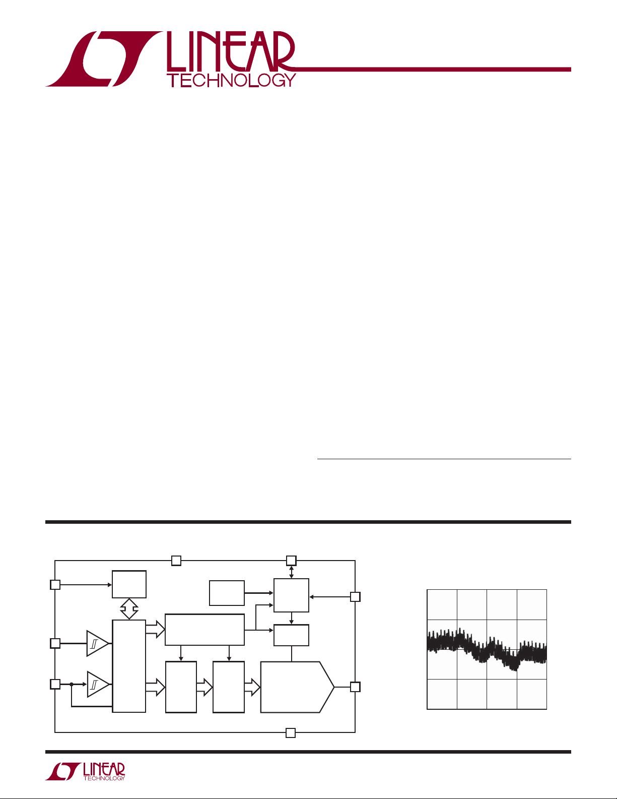
BLOCK DIAGRAM
CA0
SCL
SDA
I2C
ADDRESS
DECODE
I2C
INTERFACE
REGISTER
(LTC2631-M)
V
CC
CONTROL
DECODE LOGIC
INPUT
INTERNAL
REFERENCE
DAC
REGISTER
SWITCH
RESISTOR
DIVIDER
DACREF
DAC
GND
REF
REF_SEL
V
OUT
2631 TA01
Integral Nonlinearity (LTC2631A-LM12)
1.0
VCC = 3V
V
= 2.5V
FS
0.5
0
INL (LSB)
–0.5
–1.0
0
1024
2048
CODE
3072
4095
2631 TA01b
2631fb
1
Page 2
LTC2631
ABSOLUTE MAXIMUM RATINGS
(Notes 1, 2)
Supply Voltage (VCC) ...................................–0.3V to 6V
REF_SEL, SCL, SDA .....................................–0.3V to 6V
, CA0, CA1, REF .........–0.3V to Min(V
V
OUT
+ 0.3V, 6V)
CC
Operating Temperature Range
LTC2631C ................................................0°C to 70°C
LTC2631I..............................................–40°C to 85°C
LTC2631H (Note 3) ............................ –40°C to 125°C
PIN CONFIGURATION
Maximum Junction Temperature........................... 150°C
Storage Temperature Range ................... –65°C to 150°C
Lead Temperature (Soldering, 10 sec) ..................300°C
LTC2631-Z LTC2631-M
CA0 1
SCL 2
SDA 3
GND 4
T
JMAX
TOP VIEW
8 CA1
7 V
OUT
6 REF
5 V
CC
TS8 PACKAGE
8-LEAD PLASTIC TSOT-23
= 150°C (NOTE 6), θJA = 195°C/W
TOP VIEW
CA0 1
SCL 2
SDA 3
GND 4
TS8 PACKAGE
8-LEAD PLASTIC TSOT-23
T
= 150°C (NOTE 6), θJA = 195°C/W
JMAX
8 REF_SEL
7 V
OUT
6 REF
5 V
CC
2
2631fb
Page 3

ORDER INFORMATION
LTC2631 A C TS8 –L M 12 #TRM PBF
LTC2631
LEAD FREE DESIGNATOR
TAPE AND REEL
TR = 2,500-Piece Tape and Reel
TRM = 500-Piece Tape and Reel
RESOLUTION
12 = 12-Bit
10 = 10-Bit
8 = 8-Bit
POWER-ON RESET
M = Reset to Mid-Scale
Z = Reset to Zero-Scale
FULL-SCALE VOLTAGE, INTERNAL REFERENCE MODE
L = 2.5V
H = 4.096V
PACKAGE TYPE
TS8 = 8-Lead Plastic TSOT-23
TEMPERATURE GRADE
C = Commercial Temperature Range (0°C to 70°C)
I = Industrial Temperature Range (–40°C to 85°C)
H = Automotive Temperature Range (–40°C to 125°C)
ELECTRICAL GRADE (OPTIONAL)
A = ±1LSB Maximum INL (12-Bit)
PRODUCT PART NUMBER
Consult LTC Marketing for information on non-standard lead based fi nish parts.
For more information on lead free part marking, go to: http://www.linear.com/leadfree/
For more information on tape and reel specifi cations, go to: http://www.linear.com/tapeandreel/
2631fb
3
Page 4
LTC2631
PRODUCT SELECTION GUIDE
WITH INTERNAL
V
FS
PART NUMBER PART MARKING*
LTC2631A-LM12
LTC2631A-LZ12
LTC2631A-HM12
LTC2631A-HZ12
LTC2631-LM12
LTC2631-LM10
LTC2631-LM8
LTC2631-LZ12
LTC2631-LZ10
LTC2631-LZ8
LTC2631-HM12
LTC2631-HM10
LTC2631-HM8
LTC2631-HZ12
LTC2631-HZ10
LTC2631-HZ8
*The temperature grade is identifi ed by a label on the shipping container.
LT D H F
LT D H G
LT D H H
LT D H J
LT D H F
LT D H K
LT D H Q
LT D H G
LT D H M
LT D H R
LT D H H
LT D H N
LT D H S
LT D H J
LT D H P
LT D H T
REFERENCE
2.5V • (4095/4096)
2.5V • (4095/4096)
4.096V • (4095/4096)
4.096V • (4095/4096)
2.5V • (4095/4096)
2.5V • (1023/1024)
2.5V • (255/256)
2.5V • (4095/4096)
2.5V • (1023/1024)
2.5V • (255/256)
4.096V • (4095/4096)
4.096V • (1023/1024)
4.096V • (255/256)
4.096V • (4095/4096)
4.096V • (1023/1024)
4.096V • (255/256)
POWER-ON RESET
TO CODE PIN 8 RESOLUTION V
Mid-Scale
Zero
Mid-Scale
Zero
Mid-Scale
Mid-Scale
Mid-Scale
Zero
Zero
Zero
Mid-Scale
Mid-Scale
Mid-Scale
Zero
Zero
Zero
REF_SEL
CA1
REF_SEL
CA1
REF_SEL
REF_SEL
REF_SEL
CA1
CA1
CA1
REF_SEL
REF_SEL
REF_SEL
CA1
CA1
CA1
12-Bit
12-Bit
12-Bit
12-Bit
12-Bit
10-Bit
8-Bit
12-Bit
10-Bit
8-Bit
12-Bit
10-Bit
8-Bit
12-Bit
10-Bit
8-Bit
CC
2.7V – 5.5V
2.7V – 5.5V
4.5V – 5.5V
4.5V – 5.5V
2.7V – 5.5V
2.7V – 5.5V
2.7V – 5.5V
2.7V – 5.5V
2.7V – 5.5V
2.7V – 5.5V
4.5V – 5.5V
4.5V – 5.5V
4.5V – 5.5V
4.5V – 5.5V
4.5V – 5.5V
4.5V – 5.5V
MAXIMUM INL
±1LSB
±1LSB
±1LSB
±1LSB
±2.5LSB
±1LSB
±0.5LSB
±2.5LSB
±1LSB
±0.5LSB
±2.5LSB
±1LSB
±0.5LSB
±2.5LSB
±1LSB
±0.5LSB
4
2631fb
Page 5
LTC2631
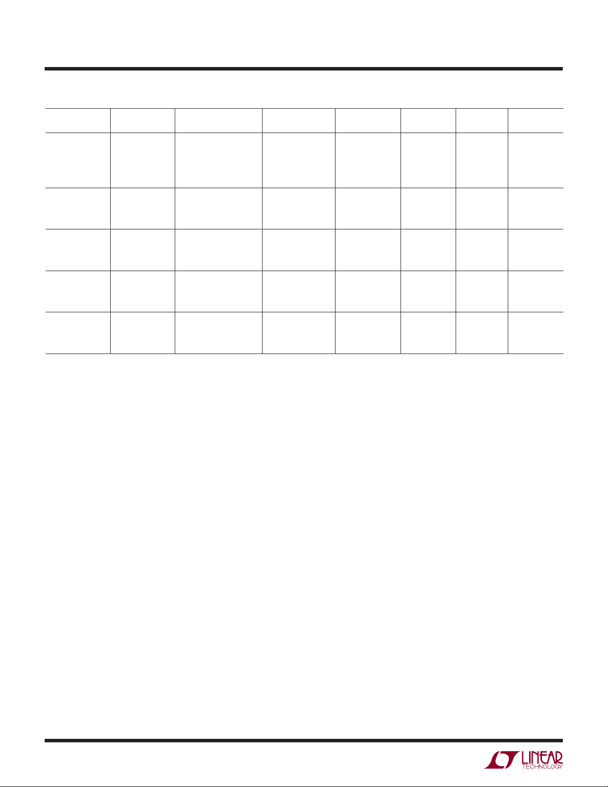
ELECTRICAL CHARACTERISTICS
The l denotes the specifi cations which apply over the full operating
temperature range, otherwise specifi cations are at T
= 25°C. VCC = 2.7V to 5.5V, V
A
LTC2631-LM12/-LM10/-LM8/-LZ12/-LZ10/-LZ8, LTC2631A-LM12/-LZ12 (VFS = 2.5V)
LTC2631-8 LTC2631-10 LTC2631-12 LTC2631A-12
SYMBOL PARAMETER CONDITIONS MIN TYP MAX MIN TYP MAX MIN TYP MAX MIN TYP MAX UNITS
DC Performance
l
Resolution
Monotonicity V
DNL Differential
= 3V, Internal Ref. (Note 4)
CC
= 3V, Internal Ref. (Note 4)
V
CC
Nonlinearity
INL Integral
VCC = 3V, Internal Ref. (Note 4)
Nonlinearity
ZSE Zero-Scale Error V
= 3V, Internal Ref.,
CC
Code = 0
V
OS
Offset Error VCC = 3V, Internal Ref.
(Note 5)
V
OSTC
VOS Temperature
Coeffi cient
VCC = 3V, Internal Ref.
(Note 5)
FSE Full-Scale Error VCC = 3V, Internal Ref.
(Note 15)
V
FSTC
Full-Scale
Voltage
Temperature
Coeffi cient
VCC = 3V, Internal Ref. (Note 10)
C-Grade
I-Grade
H-Grade
Load Regulation Internal Ref., Mid-Scale,
V
= 3V ±10%,
CC
–5mA ≤ I
V
= 5V ±10%,
CC
–10mA ≤ I
R
OUT
DC Output
Impedance
Internal Ref., Mid-Scale,
V
= 3V ±10%,
CC
–5mA ≤ I
V
= 5V ±10%,
CC
–10mA ≤ I
OUT
OUT
OUT
OUT
≤ 5mA,
≤ 10mA
≤ 5mA,
≤ 10mA
8 10 12 12 Bits
l
8 10 12 12 Bits
l
l
l
l
±0.5 ±0.5 ±1 ±1 LSB
±0.05 ±0.5 ±0.2 ±1 ±1 ±2.5 ±0.5 ±1 LSB
0.5 5 0.5 5 0.5 5 0.5 5 mV
±0.5 ±5 ±0.5 ±5 ±0.5 ±5 ±0.5 ±5 mV
±10 ±10 ±10 ±10 µV/°C
l
±0.08 ±0.4 ±0.08 ±0.4 ±0.08 ±0.4 ±0.08 ±0.4 %FSR
±10
±10
±10
l
l
l
l
0.009
0.009
0.09
0.09
0.016
0.016
0.156
0.156
unloaded unless otherwise specifi ed.
OUT
±10
±10
±10
0.035
0.035
0.09
0.09
0.064
0.064
0.156
0.156
±10
±10
±10
0.14
0.14
0.09
0.09
0.256
0.256
0.156
0.156
±10
±10
±10
0.14
0.14
0.09
0.09
0.256
0.256
0.156
0.156
ppm/°C
ppm/°C
ppm/°C
LSB/mA
LSB/mA
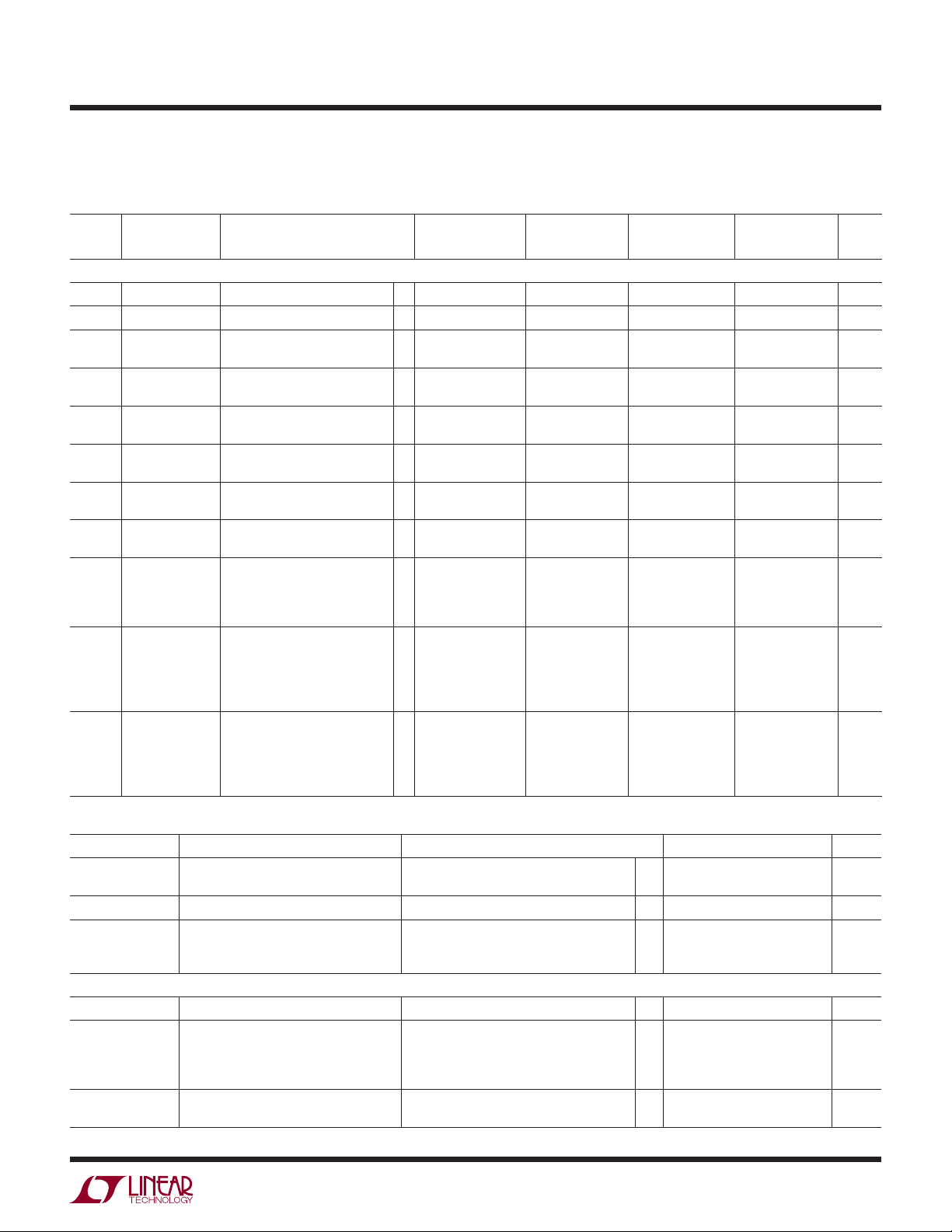
SYMBOL PARAMETER CONDITIONS MIN TYP MAX UNITS
V
OUT
DAC Output Span External Reference
PSR Power Supply Rejection V
I
SC
Short-Circuit Output Current (Note 6)
Sinking
Sourcing
Internal Reference
= 3V ±10% or 5V ±10% –80 dB
CC
VFS = VCC = 5.5V
Zero-Scale; V
Full-Scale; V
shorted to V
OUT
shorted to GND
OUT
CC
l
l
0 to V
0 to 2.5
27
–28
REF
48
–48
mA
mA
Power Supply
V
CC
I
CC
I
SD
Positive Supply Voltage For Specifi ed Performance
Supply Current (Note 7) VCC = 3V, V
V
= 3V, Internal Reference
CC
V
= 5V, V
CC
V
= 5V, Internal Reference
CC
Supply Current in Power-Down Mode
(Note 7)
VCC = 5V, C-Grade, I-Grade
V
= 5V, H-Grade
CC
= 2.5V, External Reference
REF
= 2.5V, External Reference
REF
l
2.7 5.5 V
l
l
l
l
l
l
150
180
160
190
0.6
0.6
200
240
210
260
1.8
4
µA
µA
µA
µA
µA
µA
2631fb
5
V
V
Page 6
LTC2631
The l denotes the specifi cations which apply over the full operating
ELECTRICAL CHARACTERISTICS
temperature range, otherwise specifi cations are at T
= 25°C. VCC = 2.7V to 5.5V, V
A
unloaded unless otherwise specifi ed.
OUT
LTC2631-LM12/-LM10/-LM8/-LZ12/-LZ10/-LZ8, LTC2631A-LM12/-LZ12 (V
= 2.5V)
FS
SYMBOL PARAMETER CONDITIONS MIN TYP MAX UNITS
Reference Input
Input Voltage Range
Resistance
l
l
0V
CC
160 190 220 k
Capacitance 7.5 pF
I
REF
Reference Current, Power-Down Mode DAC Powered Down
l
0.005 0.1 µA
Reference Output
l
Output Voltage
1.240 1.250 1.260 V
Reference Temperature Coeffi cient ±10 ppm/°C
Output Impedance 0.5 k
Capacitive Load Driving 10 µF
Short-Circuit Current V
= 5.5V; REF Shorted to GND 2.5 mA
CC
Digital I/O
V
IL
V
IH
V
IL(CAn)
Low Level Input Voltage (SDA and SCL) (Note 14)
High Level Input Voltage (SDA and SCL) (Note 11)
Low Level Input Voltage on CAn
See Test Circuit 1
l
–0.5 0.3V
l
0.7V
CC
l
0.15V
CC
CC
(n = 0, 1)
V
IH(CAn)
High Level Input Voltage on CAn
See Test Circuit 1
l
0.85V
CC
(n = 0, 1)
R
INH
R
INL
R
INF
V
OL
t
OF
t
SP
Resistance from CAn (n = 0, 1)
to V
to Set CAn = V
CC
CC
Resistance from CAn (n = 0, 1)
to GND to Set CA
n
= GND
Resistance from CAn (n = 0, 1)
to V
or GND to Set CAn = Float
CC
See Test Circuit 2
See Test Circuit 2
See Test Circuit 2
Low Level Output Voltage Sink Current = 3mA
Output Fall Time VO = V
C
= 10pF to 400pF (Note 12)
B
IH(MIN)
to VO = V
Pulse Width of Spikes Suppressed by
IL(MAX)
,
l
l
l
l
l
l
10 k
10 k
2M
0 0.4 V
20 + 0.1C
B
250 ns
050ns
Input Filter
I
IN
C
IN
C
B
C
CA
n
Input Leakage 0.1VCC ≤ VIN ≤ 0.9V
I/O Pin Capacitance (Note 8)
Capacitive Load for Each Bus Line
External Capacitive Load on Address
CC
l
l
l
l
±1 µA
10 pF
400 pF
10 pF
Pin CAn (n = 0, 1)
V
V
V
V
V
6
2631fb
Page 7

LTC2631
ELECTRICAL CHARACTERISTICS
The l denotes the specifi cations which apply over the full operating
temperature range, otherwise specifi cations are at T
= 25°C. VCC = 2.7V to 5.5V, V
A
LTC2631-LM12/-LM10/-LM8/-LZ12/-LZ10/-LZ8, LTC2631A-LM12/-LZ12 (VFS = 2.5V)
SYMBOL PARAMETER CONDITIONS MIN TYP MAX UNITS
AC Performance
t
S
e
n
Settling Time VCC = 3V (Note 9)
Voltage-Output Slew Rate 1 V/µs
Capacitance Load Driving 500 pF
Glitch Impulse At Mid-Scale Transition 2.1 nV•s
Multiplying Bandwidth External Reference 300 kHz
Output Voltage Noise Density At f = 1kHz, External Reference
Output Voltage Noise 0.1Hz to 10Hz, External Reference
±0.39% (±1LSB at 8-Bits)
±0.098% (±1LSB at 10-Bits)
±0.024% (±1LSB at 12-Bits)
At f = 10kHz, External Reference
At f = 1kHz, Internal Reference
At f = 10kHz, Internal Reference
0.1Hz to 10Hz, Internal Reference
0.1Hz to 200kHz, External Reference
0.1Hz to 200kHz, Internal Reference,
C
= 0.33µF
REF
unloaded unless otherwise specifi ed.
OUT
3.2
3.8
4.1
140
130
160
150
20
20
650
670
nV√Hz
nV√Hz
nV√Hz
nV√Hz
µV
P-P
µV
P-P
µV
P-P
µV
P-P
µs
µs
µs
TIMING CHARACTERISTICS
The l denotes the specifi cations which apply over the full operating temperature
range, otherwise specifi cations are at TA = 25°C. VCC = 2.7V to 5.5V. (See Figure 1) (Note 13).
LTC2631-LM12/-LM10/-LM8/-LZ12/-LZ10/-LZ8, LTC2631A-LM12/-LZ12 (VFS = 2.5V)
SYMBOL PARAMETER CONDITIONS MIN TYP MAX UNITS
f
SCL
t
HD(STA)
t
LOW
t
HIGH
t
SU(STA)
t
HD(DAT)
t
SU(DAT)
t
r
t
f
t
SU(STO)
t
BUF
SCL Clock Frequency
Hold Time (Repeated) Start Condition
Low Period of the SCL Clock Pin
High Period of the SCL Clock Pin
Set-Up Time for a Repeated Start Condition
Data Hold Time
Data Set-Up Time
Rise Time of Both SDA and SCL Signals (Note 12)
Fall Time of Both SDA and SCL Signals (Note 12)
Set-Up Time for Stop Condition
Bus Free Time Between a Stop and Start Condition
l
l
l
l
l
l
l
l
l
l
l
0 400 kHz
0.6 µs
1.3 µs
0.6 µs
0.6 µs
0 0.9 µs
100 ns
20 + 0.1C
20 + 0.1C
B
B
0.6 µs
1.3 µs
300 ns
300 ns
2631fb
7
Page 8
LTC2631
The l denotes the specifi cations which apply over the full operating
ELECTRICAL CHARACTERISTICS
temperature range, otherwise specifi cations are at T
= 25°C. VCC = 4.5V to 5.5V, V
A
unloaded unless otherwise specifi ed.
OUT
LTC2631-HM12/-HM10/-HM8/-HZ12/-HZ10/-HZ8, LTC2631A-HM12/-HZ12 (V
= 4.096V)
FS
LTC2631-8 LTC2631-10 LTC2631-12 LTC2631A-12
SYMBOL PARAMETER CONDITIONS MIN TYP MAX MIN TYP MAX MIN TYP MAX MIN TYP MAX UNITS
DC Performance
l
Resolution
Monotonicity V
DNL Differential
= 5V, Internal Ref. (Note 4)
CC
= 5V, Internal Ref. (Note 4)
V
CC
8 10 12 12 Bits
l
8 10 12 12 Bits
l
±0.5 ±0.5 ±1 ±1 LSB
Nonlinearity
INL Integral
VCC = 5V, Internal Ref. (Note 4)
l
±0.05 ±0.5 ±0.2 ±1 ±1 ±2.5 ±0.5 ±1 LSB
Nonlinearity
ZSE Zero-Scale Error V
V
V
OS
OSTC
Offset Error VCC = 5V, Internal Ref. (Note 5)
VOS Temperature
= 5V, Internal Ref., Code = 0
CC
VCC = 5V, Internal Ref. (Note 5) ±10 ±10 ±10 ±10 µV/°C
l
l
0.5 5 0.5 5 0.5 5 0.5 5 mV
±0.5 ±5 ±0.5 ±5 ±0.5 ±5 ±0.5 ±5 mV
Coeffi cient
FSE Full-Scale Error VCC = 5V, Internal Ref. (Note 15)
V
R
FSTC
OUT
Full-Scale
Voltage
Temperature
Coeffi cient
Load Regulation V
DC Output
Impedance
VCC = 5V, Internal Ref. (Note 10)
C-Grade
I-Grade
H-Grade
= 5V ±10%, Internal Ref.
CC
Mid-Scale, –10mA ≤ I
OUT
≤ 10mA
VCC = 5V ±10%, Internal Ref.
Mid-Scale, –10mA ≤ I
OUT
≤ 10mA
l
l
l
±0.08 ±0.4 ±0.08 ±0.4 ±0.08 ±0.4 ±0.08 ±0.4 %FSR
±10
±10
±10
±10
±10
±10
±10
±10
±10
±10
±10
±10
ppm/°C
ppm/°C
ppm/°C
0.006 0.01 0.022 0.04 0.09 0.16 0.09 0.16 LSB/mA
0.09 0.156 0.09 0.156 0.09 0.156 0.09 0.156
SYMBOL PARAMETER CONDITIONS MIN TYP MAX UNITS
V
OUT
DAC Output Span External Reference
PSR Power Supply Rejection V
I
SC
Short-Circuit Output Current (Note 6)
Sinking
Sourcing
Internal Reference
= 5V ±10% –80 dB
CC
VFS = VCC = 5.5V
Zero-Scale; V
Full-Scale; V
shorted to V
OUT
shorted to GND
OUT
CC
l
l
0 to V
REF
0 to 4.096
27
–28
48
–48
mA
mA
Power Supply
V
CC
I
CC
I
SD
Positive Supply Voltage For Specifi ed Performance
Supply Current (Note 7) VCC = 5V, V
V
= 5V, Internal Reference
CC
Supply Current in Power-Down Mode
(Note 7)
VCC = 5V, C-Grade, I-Grade
V
= 5V, H-Grade
CC
= 4.096V, External Reference
REF
l
4.5 5.5 V
l
l
l
l
160
200
0.6
0.6
220
270
1.8
4
µA
µA
µA
µA
2631fb
V
V
8
Page 9
LTC2631
ELECTRICAL CHARACTERISTICS
The l denotes the specifi cations which apply over the full operating
temperature range, otherwise specifi cations are at T
= 25°C. VCC = 4.5V to 5.5V, V
A
unloaded unless otherwise specifi ed.
OUT
LTC2631-HM12/-HM10/-HM8/-HZ12/-HZ10/-HZ8, LTC2631A-HM12/-HZ12 (V
= 4.096V)
FS
SYMBOL PARAMETER CONDITIONS MIN TYP MAX UNITS
Reference Input
Input Voltage Range
Resistance
l
l
0V
CC
160 190 220 k
Capacitance 7.5 pF
I
REF
Reference Current, Power-Down Mode DAC Powered Down
l
0.005 0.1 µA
Reference Output
l
Output Voltage
2.032 2.048 2.064 V
Reference Temperature Coeffi cient ±10 ppm/°C
Output Impedance 0.5 k
Capacitive Load Driving 10 µF
Short-Circuit Current V
= 5.5V; REF Shorted to GND 4.3 mA
CC
Digital I/O
V
IL
V
IH
V
IL(CAn)
Low Level Input Voltage (SDA and SCL) (Note 14)
High Level Input Voltage (SDA and SCL) (Note 11)
Low Level Input Voltage on CAn
See Test Circuit 1
l
–0.5 0.3V
l
0.7V
CC
l
0.15V
CC
CC
(n = 0, 1)
V
IH(CAn)
High Level Input Voltage on CAn
See Test Circuit 1
l
0.85V
CC
(n = 0, 1)
R
INH
R
INL
R
INF
V
OL
t
OF
t
SP
Resistance from CAn (n = 0, 1)
to V
to Set CAn = V
CC
CC
Resistance from CAn (n = 0, 1)
to GND to Set CA
n
= GND
Resistance from CAn (n = 0, 1)
to V
or GND to Set CAn = Float
CC
See Test Circuit 2
See Test Circuit 2
See Test Circuit 2
Low Level Output Voltage Sink Current = 3mA
Output Fall Time VO = V
C
= 10pF to 400pF (Note 12)
B
IH(MIN)
to VO = V
Pulse Width of Spikes Suppressed by
IL(MAX)
,
l
l
l
l
l
l
10 k
10 k
2M
0 0.4 V
20 + 0.1C
B
250 ns
050ns
Input Filter
I
IN
C
IN
C
B
C
CA
n
Input Leakage 0.1VCC ≤ VIN ≤ 0.9V
I/O Pin Capacitance (Note 8)
Capacitive Load for Each Bus Line
External Capacitive Load on Address
Pin CA
n
(n = 0, 1)
CC
l
l
l
l
±1 µA
10 pF
400 pF
10 pF
V
V
V
V
V
2631fb
9
Page 10

LTC2631
The l denotes the specifi cations which apply over the full operating
ELECTRICAL CHARACTERISTICS
temperature range, otherwise specifi cations are at T
LTC2631-HM12/-HM10/-HM8/-HZ12/-HZ10/-HZ8, LTC2631A-HM12/-HZ12 (VFS = 4.096V)
SYMBOL PARAMETER CONDITIONS MIN TYP MAX UNITS
AC Performance
t
S
e
n
Settling Time VCC = 5V (Note 9)
Voltage-Output Slew Rate 1 V/µs
Capacitance Load Driving 500 pF
Glitch Impulse At Mid-Scale Transition 3.0 nV•s
Multiplying Bandwidth External Reference 300 kHz
Output Voltage Noise Density At f = 1kHz, External Reference
Output Voltage Noise 0.1Hz to 10Hz, External Reference
= 25°C. VCC = 4.5V to 5.5V, V
A
±0.39% (±1LSB at 8-Bits)
±0.098% (±1LSB at 10-Bits)
±0.024% (±1LSB at 12-Bits)
At f = 10kHz, External Reference
At f = 1kHz, Internal Reference
At f = 10kHz, Internal Reference
0.1Hz to 10Hz, Internal Reference
0.1Hz to 200kHz, External Reference
0.1Hz to 200kHz, Internal Reference,
C
= 0.33µF
REF
unloaded unless otherwise specifi ed.
OUT
3.7
4.2
4.6
140
130
210
200
20
20
650
670
nV√Hz
nV√Hz
nV√Hz
nV√Hz
µV
P-P
µV
P-P
µV
P-P
µV
P-P
µs
µs
µs
10
2631fb
Page 11

LTC2631
TIMING CHARACTERISTICS
The l denotes the specifi cations which apply over the full operating temperature
range, otherwise specifi cations are at T
LTC2631-HM12/-HM10/-HM8/-HZ12/-HZ10/-HZ8, LTC2631A-HM12/-HZ12 (VFS = 4.096V)
SYMBOL PARAMETER CONDITIONS MIN TYP MAX UNITS
f
SCL
t
HD(STA)
t
LOW
t
HIGH
t
SU(STA)
t
HD(DAT)
t
SU(DAT)
t
r
t
f
t
SU(STO)
t
BUF
SCL Clock Frequency
Hold Time (Repeated) Start Condition
Low Period of the SCL Clock Pin
High Period of the SCL Clock Pin
Set-Up Time for a Repeated Start Condition
Data Hold Time
Data Set-Up Time
Rise Time of Both SDA and SCL Signals (Note 12)
Fall Time of Both SDA and SCL Signals (Note 12)
Set-Up Time for Stop Condition
Bus Free Time Between a Stop and Start Condition
= 25°C. VCC = 4.5V to 5.5V. (See Figure 1) (Note 13).
A
l
l
l
l
l
l
l
l
l
l
l
0 400 kHz
0.6 µs
1.3 µs
0.6 µs
0.6 µs
0 0.9 µs
100 ns
20 + 0.1C
20 + 0.1C
B
B
0.6 µs
1.3 µs
300 ns
300 ns
Note 1: Stresses beyond those listed under Absolute Maximum Ratings
may cause permanent damage to the device. Exposure to any Absolute
Maximum Rating condition for extended periods may affect device
reliability and lifetime.
Note 2: All voltages are with respect to GND.
Note 3: High temperatures degrade operating lifetimes. Operating lifetime
is derated at temperatures greater than 105°C.
Note 4: Linearity and monotonicity are defi ned from code k
N
2
– 1, where N is the resolution and kL is given by kL = 0.016 • (2N/ VFS),
rounded to the nearest whole code. For V
= 2.5V and N = 12, kL = 26 and
FS
linearity is defi ned from code 26 to code 4,095. For V
N = 12, k
= 16 and linearity is defi ned from code 16 to code 4,095.
L
to code
L
= 4.096V and
FS
Note 5: Inferred from measurement at code 16 (LTC2631-12), code 4
(LTC2631-10) or code 1 (LTC2631-8), and at full-scale.
Note 6: This IC includes current limiting that is intended to protect the
device during momentary overload conditions. Junction temperature can
exceed the rated maximum during current limiting. Continuous operation
above the specifi ed maximum operating junction temperature may impair
device reliability.
Note 7: Digital inputs at 0V or V
CC
.
Note 8: Guaranteed by design and not production tested.
Note 9: Internal Reference mode. DAC is stepped 1/4 scale to 3/4 scale
and 3/4 scale to 1/4 scale. Load is 2k in parallel with 100pF to GND.
Note 10: Temperature coeffi cient is calculated by dividing the maximum
change in output voltage by the specifi ed temperature range.
Note 11: Maximum V
Note 12: C
= capacitance of one bus line in pF
B
Note 13: All values refer to V
Note 14: Minimum V
= V
IH
exceeds the Absolute Maximum rating. This
IL
CC(MAX)
= V
IH
+ 0.5V
IH(MIN)
and VIL = V
IL(MAX)
levels.
condition won’t damage the IC, but could degrade performance.
Note 15: Full-scale error is determined using the reference voltage
measured at the REF pin.
2631fb
11
Page 12

LTC2631
TYPICAL PERFORMANCE CHARACTERISTICS
LTC2631-L12 (Internal Reference, VFS = 2.5V)
Integral Nonlinearity (INL) Differential Nonlinearity (DNL)
1.0
VCC = 3V
0.5
0
INL (LSB)
–0.5
–1.0
0
1024
INL vs Temperature
1.0
VCC = 3V
2048
CODE
3072
4095
2631 G01
1.0
VCC = 3V
0.5
0
DNL (LSB)
–0.5
–1.0
0
1024
DNL vs Temperature
1.0
VCC = 3V
2048
CODE
3072
TA = 25°C, unless otherwise noted.
Reference Output Voltage
vs Temperature
1.260
VCC = 3V
1.255
(V)
1.250
REF
V
1.245
2631 G02
4095
1.240
–50 –25 25 75 125
0
50
TEMPERATURE (°C)
Full-Scale Output Voltage
vs Temperature
2.52
VCC = 3V
100
150
2631 G03
0.5
INL (LSB)
–0.5
–1.0
INL (POS)
0
INL (NEG)
–50 –25 25 75 125
0
50
TEMPERATURE (°C)
Settling to ±1LSB
SCL
2V/DIV
3.6µs
V
OUT
1LSB/DIV
100
9th CLOCK OF
3rd DATA BYTE
150
2631 G04
1/4 SCALE TO 3/4 SCALE STEP
= 3V, VFS = 2.5V
V
CC
= 2k, CL = 100pF
R
L
AVERAGE OF 256 EVENTS
2µs/DIV
0.5
DNL (POS)
0
DNL (LSB)
–0.5
–1.0
DNL (NEG)
–50 –25 25 75 125
0
2631 G07
50
TEMPERATURE (°C)
V
OUT
1LSB/DIV
SCL
2V/DIV
100
150
2631 G05
Settling to ±1LSB
3/4 SCALE TO 1/4 SCALE STEP
= 3V, VFS = 2.5V
V
CC
= 2k, CL = 100pF
R
L
AVERAGE OF 256 EVENTS
4.1µs
9th CLOCK OF
3rd DATA BYTE
2µs/DIV
2.51
2.50
FS OUTPUT VOLTAGE (V)
2.49
2.48
–50 –25 25 75 125
0
2631 G08
50
TEMPERATURE (°C)
100
150
2631 G06
12
2631fb
Page 13

LTC2631
TYPICAL PERFORMANCE CHARACTERISTICS
3072
= 4.096V)
FS
4095
2631 G09
1.0
VCC = 5V
0.5
0
DNL (LSB)
–0.5
–1.0
0
1024
DNL vs Temperature
1.0
VCC = 5V
2048
CODE
3072
LTC2631-H12 (Internal Reference, V
Integral Nonlinearity (INL) Differential Nonlinearity (DNL)
1.0
VCC = 5V
0.5
0
INL (LSB)
–0.5
–1.0
0
1024
2048
CODE
INL vs Temperature
1.0
VCC = 5V
TA = 25°C, unless otherwise noted.
Reference Output Voltage
vs Temperature
2.068
VCC = 5V
2.058
(V)
2.048
REF
V
2.038
2631 G10
4095
2.028
–50 –25 25 75 125
0
50
TEMPERATURE (°C)
Full-Scale Output Voltage
vs Temperature
4.115
VCC = 5V
100
150
2631 G11
0.5
INL (LSB)
–0.5
–1.0
INL (POS)
0
INL (NEG)
–50 –25 25 75 125
0
50
TEMPERATURE (°C)
Settling to ±1LSB
SCL
5V/DIV
V
OUT
1LSB/DIV
3.9µs
100
9th CLOCK OF
3rd DATA BYTE
150
2631 G12
1/4 SCALE TO 3/4 SCALE STEP
= 5V, VFS = 4.095V
V
CC
= 2k, CL = 100pF
R
L
AVERAGE OF 256 EVENTS
2µs/DIV
0.5
DNL (POS)
0
DNL (LSB)
–0.5
–1.0
DNL (NEG)
–50 –25 25 75 125
0
2631 G15
50
TEMPERATURE (°C)
V
OUT
1LSB/DIV
SCL
5V/DIV
100
150
2631 G13
Settling to ±1LSB
3/4 SCALE TO 1/4 SCALE STEP
= 5V, VFS = 4.095V
V
CC
= 2k, CL = 100pF
R
L
AVERAGE OF 256 EVENTS
4.6µs
9th CLOCK OF
3rd DATA BYTE
2µs/DIV
4.105
4.095
FS OUTPUT VOLTAGE (V)
4.085
4.075
–50 –25 25 75 125
0
2631 G16
50
TEMPERATURE (°C)
100
150
2631 G14
2631fb
13
Page 14

LTC2631
TYPICAL PERFORMANCE CHARACTERISTICS
LTC2631-10
Integral Nonlinearity (INL) Differential Nonlinearity (DNL)
LTC2631-8
1.0
VCC = 5V
= 4.096V
V
FS
INTERNAL REF.
0.5
0
INL (LSB)
–0.5
–1.0
0
256
512
CODE
768
1023
2631 G17
Integral Nonlinearity (INL) Differential Nonlinearity (DNL)
1.0
VCC = 3V
= 2.5V
V
FS
INTERNAL REF.
0.5
1.0
0.5
0
DNL (LSB)
–0.5
–1.0
0
0.50
0.25
VCC = 5V
V
INTERNAL REF.
VCC = 3V
V
INTERNAL REF.
TA = 25°C, unless otherwise noted.
= 4.096V
FS
= 2.5V
FS
256
512
CODE
768
2631 G18
1023
LTC2631
0
INL (LSB)
–0.5
–1.0
0
64
128
CODE
192
255
2631 G19
0
DNL (LSB)
–0.25
–0.50
0
Load Regulation Current Limiting
10
VCC = 5V (LTC2631-H)
8
= 5V (LTC2631-L)
V
CC
= 3V (LTC2631-L)
V
CC
6
4
2
(mV)
0
OUT
–2
ΔV
–4
–6
–8
–10
–30 –20 –10 0 10 20 30
INTERNAL REF.
CODE = MIDSCALE
I
(mA)
OUT
2631 G21
0.20
VCC = 5V (LTC2631-H)
= 5V (LTC2631-L)
V
CC
0.15
= 3V (LTC2631-L)
V
CC
0.10
0.05
(V)
0
OUT
$V
–0.05
–0.10
–0.15
–0.20
–30 –20 –10 0 10 20 30
I
128
CODE
OUT
64
192
INTERNAL REF.
CODE = MIDSCALE
(mA)
255
2631 G20
2631 G22
14
2631fb
Page 15

LTC2631
TYPICAL PERFORMANCE CHARACTERISTICS
LTC2631
Offset Error vs Temperature
3
2
1
0
–1
OFFSET ERROR (mV)
–2
–3
–50 –25 0 25 50 75 100 125 150
TEMPERATURE (°C)
Large-Signal Response
2631 G23
Gain Error vs V
0.4
0.3
0.2
0.1
0.0
–0.1
GAIN ERROR (%FSR)
–0.2
–0.3
–0.4
2.5 3 3.5 4 4.5 5 5.5
CC
EXTERNAL REF.
V
VCC (V)
Mid-Scale-Glitch Impulse Power-On Reset Glitch
9th CLOCK OF
3rd DATA BYTE
SCL
5V/DIV
TA = 25°C, unless otherwise noted.
Gain Error vs Temperature
0.4
= 2.5V
REF
2631 G24
0.3
0.2
0.1
0.0
–0.1
GAIN ERROR (%FSR)
–0.2
–0.3
–0.4
–50 –25 0 25 50 75 100 125 150
TEMPERATURE (°C)
LTC2631-L
V
CC
2V/DIV
EXTERNAL REF.
= 2.5V
V
REF
2631 G25
V
OUT
0.5V/DIV
VFS = VCC = 5V
1/4 SCALE TO 3/4 SCALE
2µs/DIV
Headroom at Rails
vs Output Current Exiting Power-Down to Mid-Scale
5.0
4.5
4.0
3.5
3.0
(V)
2.5
OUT
V
2.0
1.5
1.0
0.5
0
012345678910
2631 G26
5V SOURCING
3V (LTC2631-L) SOURCING
5V SINKING
3V (LTC2631-L) SINKING
I
(mA)
OUT
V
OUT
5mV/DIV
2631 G29
LTC2631-H12, VCC = 5V:
3.0nV-s TYP
LTC2631-L12, VCC = 3V:
2.1nV-s TYP
2µs/DIV
CS/LD
2V/DIV
V
OUT
0.5V/DIV
2631 G27
V
2mV/DIV
4µs/DIV
OUT
LTC2631-H
2631 G30
ZERO-SCALE
200µs/DIV
2631 G28
2631fb
15
Page 16

LTC2631
TYPICAL PERFORMANCE CHARACTERISTICS
LTC2631
Supply Current
Supply Current vs Logic Voltage
1.2
1.0
0.8
0.6
(mA)
CC
I
0.4
0.2
0.0
0
SWEEP SCL AND SDA
BETWEEN 0V AND V
VCC = 3V
(LTC2631-L)
LOGIC VOLTAGE (V)
CC
VCC = 5V
531
42
2631 G31
Multiplying Bandwidth
0
–2
–4
–6
–8
dB
–10
–12
VCC = 5V
–14
–16
–18
1k
= 2V
V
REF(DC)
= 0.2V
V
REF(AC)
CODE = FULL SCALE
P-P
FREQUENCY (Hz)
vs REF_SEL Voltage
0.5
0.4
0.3
(mA)
CC
I
0.2
0.1
0
100k
TA = 25°C, unless otherwise noted.
SWEEP REF_SEL
BETWEEN 0V AND V
VCC = 5V
VCC = 3V
(LTC2631-L)
REF_SEL VOLTAGE (V)
1000k10k
2631 G33
CC
531
42
2631 G32
16
Noise Voltage vs Frequency
500
INTERNAL REF.
CODE = MIDSCALE
400
300
LTC2631-H
= 5V)
(V
200
NOISE VOLTAGE (nV/√Hz)
100
0
100
CC
LTC2631-L
(V
CC
1k
FREQUENCY (Hz)
= 4V)
10k
100k
2631 G34
1M
10µV/DIV
0.1Hz to 10Hz Voltage Noise
LTC2631-L, VCC = 4V
INTERNAL REF.
CODE = MIDSCALE
1s/DIV
2631 G35
2631fb
Page 17

PIN FUNCTIONS
LTC2631
CA0 (Pin 1): Chip Address Bit 0. Tie this pin to VCC, GND
or leave it fl oating to select an I
part (see Tables 1 and 2).
SCL (Pin 2): Serial Clock Input Pin. Data is shifted into
the SDA pin at the rising edges of the clock. This high
impedance pin requires a pull-up resistor or current
source to V
SDA (Pin 3): Serial Data Bidirectional Pin. Data is shifted
into the SDA pin and acknowledged by the SDA pin. This
pin is high impedance while data is shifted in. Open-drain
N-channel output during acknowledgment. SDA requires
a pull-up resistor or current source to V
GND (Pin 4): Ground.
(Pin 5): Supply Voltage Input. 2.7V ≤ VCC ≤ 5.5V
V
CC
(LTC2631-L) or 4.5V ≤ V
to GND with a 0.1µF capacitor.
CC
.
CC
2
C slave address for the
.
CC
≤ 5.5V (LTC2631-H). Bypass
REF (Pin 6): Reference Voltage Input or Output. When
External Reference mode is selected, REF is an input (0V
≤ V
scale voltage. When Internal Reference is selected, the
10ppm/°C 1.25V (LTC2631-L) or 2.048V (LTC2631-H)
internal reference is available at the pin. This output may
be bypassed to GND with up to 10µF (0.33µF is recommended), and must be buffered when driving external DC
load current.
V
CA1 (Pin 8, LTC2631-Z): Chip Address Bit 1. Tie this pin
to V
dress for the part (see Table 1).
REF_SEL (Pin 8, LTC2631-M): Selects default Reference
at power up. Tie to V
or GND to select an External Reference. After power-up,
the logic state at this pin is ignored and the reference may
be changed only by software command.
≤ VCC) where the voltage supplied sets the full-
REF
(Pin 7): DAC Analog Voltage Output.
OUT
, GND or leave it fl oating to select an I2C slave ad-
CC
to select the Internal Reference,
CC
2631fb
17
Page 18

LTC2631
BLOCK DIAGRAMS
LTC2631-Z
CA1
CA0
SCL
SDA
CA0
I2C
ADDRESS
DECODE
I2C
INTERFACE
I2C
ADDRESS
DECODE
V
CC
DECODE LOGIC
INPUT
REGISTER
LTC2631-M
V
CC
CONTROL
INTERNAL
REFERENCE
DAC
REGISTER
INTERNAL
REFERENCE
SWITCH
RESISTOR
DIVIDER
DACREF
DAC
GND
SWITCH
REF
REF
V
OUT
REF_SEL
SCL
SDA
I2C
INTERFACE
DECODE LOGIC
INPUT
REGISTER
CONTROL
DAC
REGISTER
RESISTOR
DIVIDER
DACREF
DAC
GND
V
OUT
2631 BD
2631fb
18
Page 19

TEST CIRCUITS
Test Circuits for I2C Digital I/O (See Electrical Characteristics)
Test Circuit 2Test Circuit 1
LTC2631
V
CC
100Ω
V
IH(CAn)/VIL(CAn)
CAn
R
INH/RINL/RINF
CAn
GND
2631 TC
2631fb
19
Page 20

LTC2631
TIMING DIAGRAMS
2631 F02
ACK
2631 F01
SDA
BUF
t
r
t
SU(STO)
SCL
t
S P S
SU(STA)
t
LEVELS
IL(MAX)
HIGH
t
AND V
IH(MIN)
HD(DAT)
t
HD(STA)
t
S
ALL VOLTAGE LEVELS REFER TO V
Figure 1. Serial Interface Timing
SP
t
HD(STA)
t
f
t
SU(DAT)
t
r
t
LOW
t
f
t
ACK
1ST DATA BYTE 2ND DATA BYTE 3RD DATA BYTE
C2C3 C1 C0 X X X X XXXX
ACK ACK
Figure 2. Typical LTC2631 Write Transaction
20
A2 A1 A0 W
SLAVE ADDRESS
A6 A5 A4 A3
START
SDA
123456789123456789123456789123456789
SCL
2631fb
Page 21

OPERATION
LTC2631
The LTC2631 is a family of single voltage-output DACs in
8-lead ThinSOT packages. Each DAC can operate rail-to-rail
using an external reference, or with its full-scale voltage
set by an integrated reference. Twelve combinations of
accuracy (12-, 10-, and 8-bit), power-on reset value (zero
or mid-scale), and full-scale voltage (2.5V or 4.096V) are
2
available. The LTC2631 is controlled using a 2-wire I
C
interface.
Power-On Reset
The LTC2631-HZ/LTC2631-LZ clear the output to zero-scale
when power is fi rst applied, making system initialization
consistent and repeatable.
For some applications, downstream circuits are active
during DAC power-up, and may be sensitive to nonzero
outputs from the DAC during this time. The LTC2631
contains circuitry to reduce the power-on glitch: the analog
output typically rises less than 5mV above zero-scale
during power on if the power supply is ramped to 5V in
1ms or more. In general, the glitch amplitude decreases as
the power supply ramp time is increased. See “Power-On
Reset Glitch” in the Typical Performance Characteristics
section.
The LTC2631-HM/LTC2631-LM provide an alternative
reset, setting the output to mid-scale when power is fi rst
applied.
code, N is the resolution, and V
is either 2.5V (LTC2631-
REF
LM/LTC2631-LZ) or 4.096V (LTC2631-HM/LTC2631-HZ)
when in Internal Reference mode, and the voltage at REF
(Pin 6) when in External Reference mode.
2
C Serial Interface
I
The LTC2631 communicates with a host using the stan-
2
dard 2-wire I
C interface. The Timing Diagrams (Figures 1
and 2) show the timing relationship of the signals on the
bus. The two bus lines, SDA and SCL, must be high when
the bus is not in use. External pull-up resistors or current
sources are required on these lines. The value of these
pull-up resistors is dependent on the power supply and
2
can be obtained from the I
C specifi cations. For an I2C
bus operating in the fast mode, an active pull-up will be
necessary if the bus capacitance is greater than 200pF.
The LTC2631 is a receive-only (slave) device. The master
can write to the LTC2631. The LTC2631 does not respond
to a read from the master.
START (S) and STOP (P) Conditions
When the bus is not in use, both SCL and SDA must be
high. A bus master signals the beginning of a communication to a slave device by transmitting a START condition.
A START condition is generated by transitioning SDA from
high to low while SCL is high.
Default reference mode selection is described in the Reference Modes section.
Power Supply Sequencing
The voltage at REF (Pin 6) should be kept within the range
– 0.3V ≤ V
≤ VCC + 0.3V (see Absolute Maximum Rat-
REF
ings). Particular care should be taken to observe these
limits during power supply turn-on and turn-off sequences,
when the voltage at V
(Pin 5) is in transition.
CC
Transfer Function
The digital-to-analog transfer function is
V
OUT(IDEAL)
k
⎛
⎞
=
V
⎜
⎝
REF
⎟
N
⎠
2
where k is the decimal equivalent of the binary DAC input
When the master has fi nished communicating with the
slave, it issues a STOP condition. A STOP condition is
generated by transitioning SDA from low to high while
SCL is high. The bus is then free for communication with
2
another I
C device.
Acknowledge
The Acknowledge signal is used for handshaking between
the master and the slave. An Acknowledge (active LOW)
generated by the slave lets the master know that the
latest byte of information was properly received. The
Acknowledge related clock pulse is generated by the
master. The master releases the SDA line (HIGH) during
the Acknowledge clock pulse. The slave-receiver must pull
down the SDA bus line during the Acknowledge clock pulse
so that it remains a stable LOW during the HIGH period
of this clock pulse. The LTC2631 responds to a write by a
2631fb
21
Page 22

LTC2631
OPERATION
master in this manner but does not acknowledge a read
operation; in that case, SDA is retained HIGH during the
period of the Acknowledge clock pulse.
Chip Address
The state of pins CA0 and CA1 (LTC2631-HZ/LTC2631LZ) determines the slave address of the part. These pins
can each be set to any one of three states: V
, GND or
CC
fl oat. This results in nine (LTC2631-HZ/LTC2631-LZ) or
three (LTC2631-HM/LTC2631-LM) selectable addresses
for the part. The slave address assignments are shown
in Tables 1 and 2.
Table 1. Slave Address Map (LTC2631-Z)
CA1 CA0 A6 A5 A4 A3 A2 A1 A0
GND GND 0 0 1 0 0 0 0
GND FLOAT 0 0 1 0 0 0 1
GND V
FLOAT GND 0 0 1 0 0 1 1
FLOAT FLOAT 0 1 0 0 0 0 0
FLOAT V
V
CC
V
CC
V
CC
GLOBAL ADDRESS 1 1 1 0 0 1 1
Table 2. Slave Address Map (LTC2631-M)
FLOAT 0 0 1 0 0 0 1
GLOBAL ADDRESS 1 1 1 0 0 1 1
CC
CC
GND 0 1 0 0 0 1 0
FLOAT 0 1 0 0 0 1 1
V
CC
CA0 A6 A5 A4 A3 A2 A1 A0
GND 0 0 1 0 0 0 0
V
CC
0010010
0100001
0110000
0010010
In addition to the address selected by the address pins, the
part also responds to a global address. This address allows
a common write to all LTC2631 parts to be accomplished
2
using one 3-byte write transaction on the I
C bus. The
global address, listed at the end of Tables 1 and 2, is a 7-bit
hardwired address not selectable by CA0/CA1. If another
address is required, please consult the factory.
The maximum capacitive load allowed on the CA0/CA1
address pins is 10pF, as these pins are driven during address detection to determine if they are fl oating.
Write Word Protocol
The master initiates communication with the LTC2631
with a START condition and a 7-bit slave address followed
by the Write bit (W) = 0. The LTC2631 acknowledges by
pulling the SDA pin low at the ninth clock if the 7-bit slave
address matches the address of the part (set by CA0/CA1)
or the global address. The master then transmits 3-bytes
of data. The LTC2631 acknowledges each byte of data by
pulling the SDA line low at the ninth clock of each data
byte transmission. After receiving three complete bytes
of data, the LTC2631 executes the command specifi ed in
the 24-bit input word.
If more than three data bytes are transmitted after a valid
7-bit slave address, the LTC2631 does not acknowledge the
extra bytes of data (SDA is high during the 9th clock).
The format of the three data bytes is shown in Figure 3. The
fi rst byte of the input word consists of the 4-bit command,
followed by four don’t-cares bits. The next two bytes
contain the 16-bit data word, which consists of the 12-,
10- or 8-bit input code, MSB to LSB, followed by 4, 6 or 8
don’t-cares bits (LTC2631-12, LTC2631-10 and LTC2631-8
respectively). A typical LTC2631 write transaction is
shown in Figure 4.
The command bit assignments (C3-C0) are shown in
Table 3. The fi rst four commands in the table consist of
write and update operations. A write operation loads a
16-bit data word from the 32-bit shift register into the
input register. In an update operation, the data word is
copied from the input register to the DAC register and
converted to an analog voltage at the DAC output. The
update operation also powers up the DAC if it had been in
power-down mode. The data path and registers are shown
in the Block Diagram.
22
2631fb
Page 23

OPERATION
Write Word Protocol for LTC2631
WA
S
SLAVE ADDRESS
1ST DATA BYTE
LTC2631
A 2ND DATA BYTE A 3RD DATA BYTE A P
Input Word (LTC2631-12)
X
C2
C2
C2
C1
C0
1ST DATA BYTE
C1
C0
1ST DATA BYTE
C1
C0
1ST DATA BYTE
C3
Input Word (LTC2631-10)
C3
Input Word (LTC2631-8)
C3
X
X
X
X
X
X
X
X
X
X
X
Figure 3. Command and Data Input Format
Table 3. Command Codes
COMMAND*
C3 C2 C1 C0
0 0 0 0 Write to Input Register
0 0 0 1 Update (Power Up) DAC Register
0 0 1 1 Write to and Update (Power Up) DAC Register
0 1 0 0 Power Down
0 1 1 0 Select Internal Reference
0 1 1 1 Select External Reference
*Command codes not shown are reserved and should not be used.
INPUT WORD
D8
D7 D6 D5 D4
D9D10D11
2ND DATA BYTE
D6
D5 D4 D3 D2
D7D8D9
2ND DATA BYTE 3RD DATA BYTE
D4
D3 D2 D1 D0
D5D6D7
2ND DATA BYTE 3RD DATA BYTE
D2
D1 D0 X X X
D3
D0
D1
X
X
3RD DATA BYTE
XXXXX
XXXXX
to the REF pin will improve noise performance; 0.33µF
is recommended, and up to 10µF can be driven without
oscillation. This output must be buffered when driving
external DC load current.
Alternatively, the DAC can operate in External Reference
mode using command 0111. In this mode, an input voltage
supplied externally to the REF pin provides the reference
(0V ≤ V
≤ VCC) and the supply current is reduced.
REF
External Reference mode is the power-on default for
LTC2631-HM/LTC2631-LM when REF_SEL is tied low.
X
X
X
2631 F03
Reference Modes
For applications where an accurate external reference is
not available, the LTC2631 has a user-selectable, integrated
reference. The LTC2631-LM/LTC2631-LZ provide a fullscale output of 2.5V. The LTC2631-HM/LTC2631-HZ provide
a full-scale output of 4.096V. The internal reference can be
useful in applications where the supply voltage is poorly
regulated. Internal Reference mode can be selected by using
command 0110, and is the power-on default for LTC2631HZ/LTC2631-LZ, as well as for LTC2631-HM/LTC2631-LM
when REF_SEL is tied high.
The 10ppm/°C, 1.25V (LTC2631-LM/LTC2631-LZ) or
2.048V (LTC2631-HM/LTC2631-HZ) internal reference
is available at the REF pin. Adding bypass capacitance
The reference mode of LTC2631-HZ/LTC2631-LZ can be
changed only by software command. The same is true for
LTC2631-HM/LTC2631-LM after power-on, after which the
logic state on REF_SEL is ignored.
Power-Down Mode
For power-constrained applications, the LTC2631’s powerdown mode can be used to reduce the supply current
whenever the DAC output is not needed. When in power
down, the buffer amplifi er, bias circuit, and reference
circuit are disabled and draw essentially zero current. The
DAC output is put into a high-impedance state, and the
output pin is passively pulled to ground through a 200k
resistor. Input and DAC register contents are not disturbed
during power down.
2631fb
23
Page 24

LTC2631
OPERATION
The DAC can be put into power-down mode by using
command 0100. The supply current is reduced to 1.8µA
maximum (C and I grades) and the REF pin becomes high
impedance (typically > 1G).
Normal operation resumes after executing any command
that includes a DAC update, as shown in Table 3. The
DAC is powered up and its voltage output is updated.
Normal settling is delayed while the bias, reference, and
amplifi er circuits are re-enabled. When the REF pin output
is bypassed to GND with 1nF or less, the power-up delay
time is 20µs for settling to 12-bits. This delay increases
to 200µs for 0.33µF, and 10ms for 10µF.
Voltage Output
The LTC2631’s integrated rail-to-rail amplifi er has guaranteed load regulation when sourcing or sinking up to
10mA at 5V, and 5mA at 3V.
Load regulation is a measure of the amplifi er’s ability to
maintain the rated voltage accuracy over a wide range of
load current. The measured change in output voltage per
change in forced load current is expressed in LSB/mA.
DC output impedance is equivalent to load regulation, and
may be derived from it by simply calculating a change in
units from LSB/mA to ohms. The amplifi er’s DC output
impedance is 0.1 when driving a load well away from
the rails.
When drawing a load current from either rail, the output
voltage headroom with respect to that rail is limited by
the 50 typical channel resistance of the output devices
(e.g., when sinking 1mA, the minimum output voltage is
50 • 1mA, or 50mV). See the graph “Headroom at Rails
vs. Output Current” in the Typical Performance Characteristics section.
Similarly, limiting can occur near full-scale when the REF
pin is tied to V
(FSE) is positive, the output for the highest codes limits
, as shown in Figure 5c. No full-scale limiting can
at V
CC
occur if V
Offset and linearity are defi ned and tested over the region
of the DAC transfer function where no output limiting can
occur.
Board Layout
The PC board should have separate areas for the analog and
digital sections of the circuit. A single, solid ground plane
should be used, with analog and digital signals carefully
routed over separate areas of the plane. This keeps digital
signals away from sensitive analog signals and minimizes
the interaction between digital ground currents and the
analog section of the ground plane. The resistance from
the LTC2631 GND pin to the ground plane should be as
low as possible. Resistance here will add directly to the
effective DC output impedance of the device (typically
0.1). Note that the LTC2631 is no more susceptible to this
effect than any other parts of this type; on the contrary, it
allows layout-based performance improvements to shine
rather than limiting attainable performance with excessive
internal resistance.
Another technique for minimizing errors is to use a separate power ground return trace on another board layer.
The trace should run between the point where the power
supply is connected to the board and the DAC ground pin.
Thus the DAC ground pin becomes the common point for
analog ground, digital ground, and power ground. When
the LTC2631 is sinking large currents, this current fl ows
out the ground pin and directly to the power ground trace
without affecting the analog ground plane voltage.
. If V
CC
is less than V
REF
= VCC and the DAC full-scale error
REF
– FSE.
CC
The amplifi er is stable driving capacitive loads of up to
500pF.
Rail-to-Rail Output Considerations
In any rail-to-rail voltage-output device, the output is limited to voltages within the supply range.
Since the analog output of the DAC cannot go below ground,
it may limit the lowest codes, as shown in Figure 5b.
24
It is sometimes necessary to interrupt the ground plane
to confi ne digital ground currents to the digital portion of
the plane. When doing this, make the gap in the plane only
as long as it needs to be to serve its purpose and ensure
that no traces cross over the gap.
2631fb
Page 25

LTC2631
OPERATION
2631 F04
STOP
FULL-SCALE
VOLTAGE
ZERO-SCALE
VOLTAGE
ACK
LS DATA
D3 D2 D1 D0 X X X X
ACK
MS DATA
D11 D10 D9 D8 D7 D6 D5 D4
COMMAND
C3 C2 C1 C0 X X X X
SLAVE ADDRESS
A6 A5 A4 A3 A2 A1 A0 W
91234567891234567812345678912345678 9
C1 C0 X X X X
C2C3
ACK ACK
Figure 4. Typical LTC2631 Input Waveform—Programming 12-Bit DAC Output for Full-Scale
A6 A5 A4 A3 A2 A1 A0
SCL
X = DON’T CARE
OUT
V
2631fb
START
SDA
25
Page 26

LTC2631
OPERATION
VOLTAGE
NEGATIVE
OFFSET
OUTPUT
V
= V
REF
CC
= V
V
REF
CC
OUTPUT
VOLTAGE
INPUT CODE
(c)
0V
0V
INPUT CODE
(b)
2,0480 4,095
INPUT CODE
(a)
POSITIVE
FSE
OUTPUT
VOLTAGE
2631 F05
Figure 5. Effects of Rail-to-Rail Operation on a DAC Transfer Curve (Shown for 12-Bits)
(a) Overall Transfer Function
(b) Effect of Negative Offset for Codes Near Zero
(c) Effect of Positive Full-Scale Error for Codes Near Full-Scale
26
2631fb
Page 27

PACKAGE DESCRIPTION
LTC2631
TS8 Package
8-Lead Plastic TSOT-23
(Reference LTC DWG # 05-08-1637)
0.52
MAX
3.85 MAX
2.62 REF
RECOMMENDED SOLDER PAD LAYOUT
PER IPC CALCULATOR
0.20 BSC
DATUM ‘A’
0.30 – 0.50 REF
NOTE:
1. DIMENSIONS ARE IN MILLIMETERS
2. DRAWING NOT TO SCALE
3. DIMENSIONS ARE INCLUSIVE OF PLATING
4. DIMENSIONS ARE EXCLUSIVE OF MOLD FLASH AND METAL BURR
5. MOLD FLASH SHALL NOT EXCEED 0.254mm
6. JEDEC PACKAGE REFERENCE IS MO-193
0.65
REF
1.22 REF
1.4 MIN
2.80 BSC
0.09 – 0.20
(NOTE 3)
1.50 – 1.75
(NOTE 4)
1.00 MAX
0.65 BSC
0.80 – 0.90
2.90 BSC
(NOTE 4)
PIN ONE ID
0.22 – 0.36
8 PLCS (NOTE 3)
0.01 – 0.10
1.95 BSC
TS8 TSOT-23 0802
Information furnished by Linear Technology Corporation is believed to be accurate and reliable.
However, no responsibility is assumed for its use. Linear Technology Corporation makes no representation that the interconnection of its circuits as described herein will not infringe on existing patent rights.
2631fb
27
Page 28

LTC2631
TYPICAL APPLICATION
1.7k 1.7k
I2C BUS
CA0
8
REF_SEL
3
SDA
2
SCL
1
CA0
Programmable ±5V Output
5V
0.1µF
56
VCCREF
LTC2631A
-LM12
GND
4
4
–
3
+
7
V
OUT
5V
5
LTC2054
2
0.1µF
M9
M3
M1
P1
P3
P9
10V
V
LT1991
V
EE
0.1µF
7
CC
REF
4
OUT
5
0.1µF
6
V
= ±5V
OUT
1
8
9
10
1
2
3
–10V
2631 TA03
RELATED PARTS
PART NUMBER DESCRIPTION COMMENTS
LTC1663 Single 10-Bit V
LTC1669 Single 10-Bit V
LTC2360-LT2362/
12-Bit SAR ADCs in TSOT23-6/TSOT23-8 Packages 100ksps/250ksps/500ksps/1Msps/3Msps Output Rates
LTC2365-LTC2366
LTC2450/LTC2452 16-Bit Single-Ended/Differential Delta Sigma ADCs SPI Interface, Tiny DFN Packages, 60Hz Output Rate
LTC2451/LTC2453 16-Bit Single-Ended/Differential Delta Sigma ADCs I
LTC2600/LTC2610/LTC2620 Octal 16-/14-/12-Bit V
LTC2601/LTC2611/LTC2621 Single 16-/14-/12-Bit V
LTC2602/LTC2612/LTC2622 Dual 16-/14-/12-Bit V
LTC2604/LTC2614/LTC2624 Quad 16-/14-/12-Bit V
LTC2605/LTC2615/LTC2625 Octal 16-/14-/12-Bit V
LTC2606/LTC2616/LTC2626 Single 16-/14-/12-Bit V
LTC2609/LTC2619/LTC2629 Quad 16-/14-/12-Bit V
LTC2630 Single 12-/10-/8-Bit V
Reference in SC70
LTC2640 Single 12-/10-/8-Bit SPI V
Reference in ThinSOT
DAC in SOT-23 VCC = 2.7V to 5.5V, 60µA, Internal Reference, SMBus Interface
OUT
DAC in SOT-23 VCC = 2.7V to 5.5V, 60µA, Internal Reference, I2C Interface
OUT
2
C Interface, Tiny DFN and TSOT23-8 Packages, 60Hz Output Rate
DACs in 16-Lead SSOP 250µA per DAC, 2.5V to 5.5V Supply Range, Rail-to-Rail Output,
OUT
SPI Serial Interface
DACs in 10-Lead DFN 300µA per DAC, 2.5V to 5.5V Supply Range, Rail-to-Rail Output,
OUT
SPI Serial Interface
DACs in 8-Lead MSOP 300µA per DAC, 2.5V to 5.5V Supply Range, Rail-to-Rail Output,
OUT
SPI Serial Interface
DACs in 16-Lead SSOP 250µA per DAC, 2.5V to 5.5V Supply Range, Rail-to-Rail Output,
OUT
SPI Serial Interface
DACs with I2C Interface 250µA per DAC, 2.5V to 5.5V Supply Range, Rail-to-Rail Output,
OUT
DACs with I2C Interface 270µA per DAC, 2.5V to 5.5V Supply Range, Rail-to-Rail Output,
OUT
DACs with I2C Interface 250µA per DAC, 2.5V to 5.5V Supply Range, Rail-to-Rail Output with
OUT
DACs with 10ppm/°C
OUT
2
I
C Interface
2
I
C Interface
Separate V
Pins for Each DAC
REF
180µA per DAC, 2.7V to 5.5V Supply Range, 10ppm/°C Reference,
Rail-to-Rail Output, SPI Interface
DACs with 10ppm/°C
OUT
180µA per DAC, 2.7V to 5.5V Supply Range, 10ppm/°C Reference,
Selectable External Reference Mode, Rail-to-Rail Output, SPI Interface
28
Linear Technology Corporation
1630 McCarthy Blvd., Milpitas, CA 95035-7417
(408) 432-1900 ● FAX: (408) 434-0507
●
www.linear.com
2631fb
LT 1108 REV B • PRINTED IN USA
© LINEAR TECHNOLOGY CORPORATION 2008
 Loading...