

FEATURES
■
Easy Drive Technology Enables Rail-to-Rail Inputs
with Zero Differential Input Current
■
Directly Digitizes High Impedance Sensors with
Full Accuracy
■
Programmable Gain from 1 to 256
■
Integrated Temperature Sensor
■
GND to VCC Input/Reference Common Mode Range
■
Programmable 50Hz, 60Hz or Simultaneous
50Hz/60Hz Rejection Mode
■
2ppm (0.25LSB) INL, No Missing Codes
■
1ppm Offset and 15ppm Full-Scale Error
■
Selectable 2x Speed Mode (15Hz Using Internal
Oscillator)
■
No Latency: Digital Filter Settles in a Single Cycle
■
Single Supply 2.7V to 5.5V Operation
■
Internal Oscillator
■
Available in a Tiny (3mm × 3mm) 10-Lead
DFN Package
U
APPLICATIO S
■
Direct Sensor Digitizer
■
Weight Scales
■
Direct Temperature Measurement
■
Strain Gauge Transducers
■
Instrumentation
■
Industrial Process Control
■
DVMs and Meters
LTC2480
16-Bit ∆Σ ADC with Easy Drive
Input Current Cancellation
U
DESCRIPTIO
The LTC®2480 combines a 16-bit plus sign No Latency ∆Σ
analog-to-digital converter with patented Easy DriveTM technology. The patented sampling scheme eliminates dynamic
input current errors and the shortcomings of on-chip buffering through automatic cancellation of differential input
current. This allows large external source impedances and
input signals, with rail-to-rail input range to be directly digitized while maintaining exceptional DC accuracy.
The LTC2480 includes on-chip programmable gain, a
temperature sensor and an oscillator. The LTC2480 can be
configured to provide a programmable gain from 1 to 256
in 8 steps, measure an external signal or internal temperature sensor and reject line frequencies. 50Hz, 60Hz or
simultaneous 50Hz/60Hz line frequency rejection can be
selected as well as a 2x speed-up mode.
The LTC2480 allows a wide common mode input range
(0V to V
reference can be as low as 100mV or can be tied directly
to VCC. The LTC2480 includes an on-chip trimmed oscillator eliminating the need for external crystals or oscillators. Absolute accuracy and low drift are automatically
maintained through continuous, transparent, offset and
full-scale calibration.
, LTC and LT are registered trademarks of Linear Technology Corporation.
No Latency ∆Σ and Easy Drive are trademarks of Linear Technology Corporation.
All other trademarks are the property of their respective owners.
Patent Pending.
) independent of the reference voltage. The
CC
TM
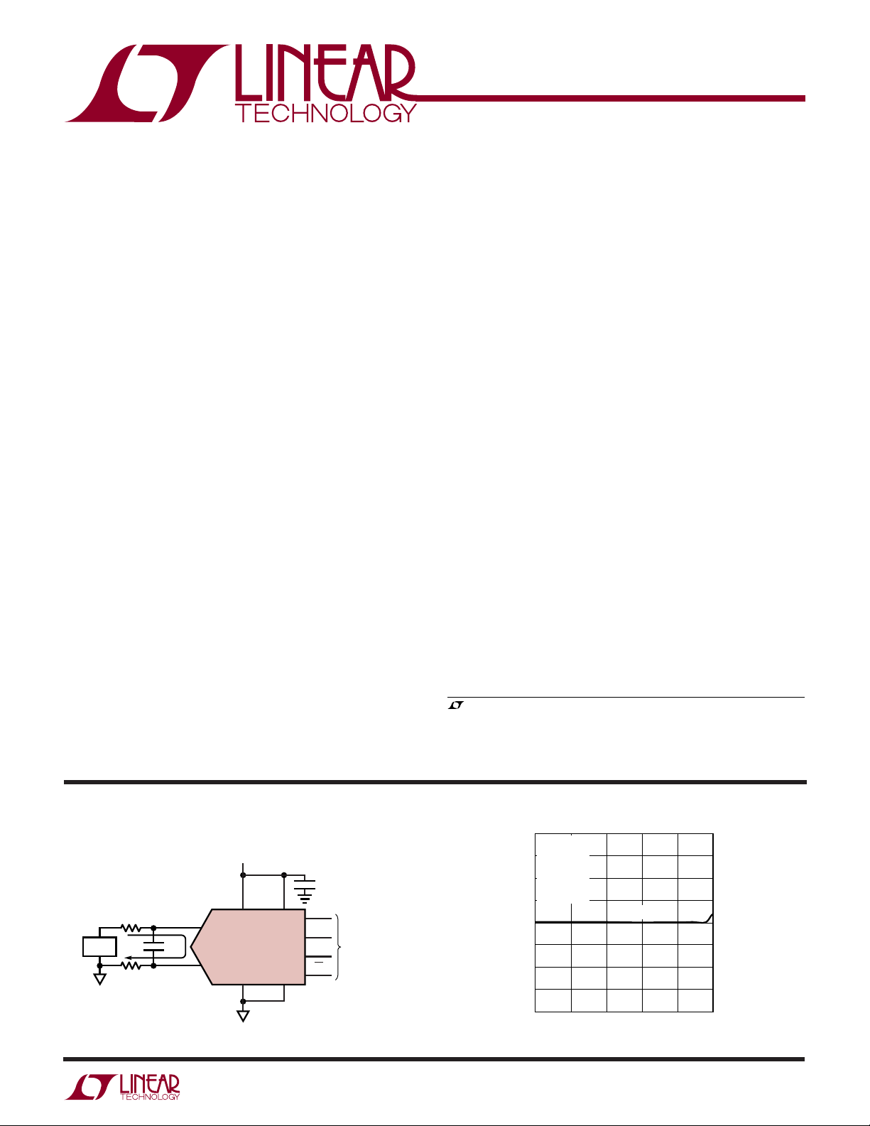
TYPICAL APPLICATIO
V
CC
SENSE
10k
10k
I
DIFF
= 0
1µF
V
IN
V
IN
V
REF
+
LTC2480
–
GND F
U
+FS Error vs R
80
VCC = 5V
= 5V
V
REF
60
+
= 3.75V
V
IN
–
= 1.25V
V
IN
40
= GND
1µF
SDI
V
CC
SDO
4-WIRE
SCK
SPI INTERFACE
CS
O
2480 TA01
F
O
= 25°C
T
A
20
0
–20
+FS ERROR (ppm)
–40
–60
–80
10 100 10k
1
R
SOURCE
CIN = 1µF
SOURCE
at IN+ and IN
1k
(Ω)
–
100k
2480 TA04
2480f
1
LTC2480
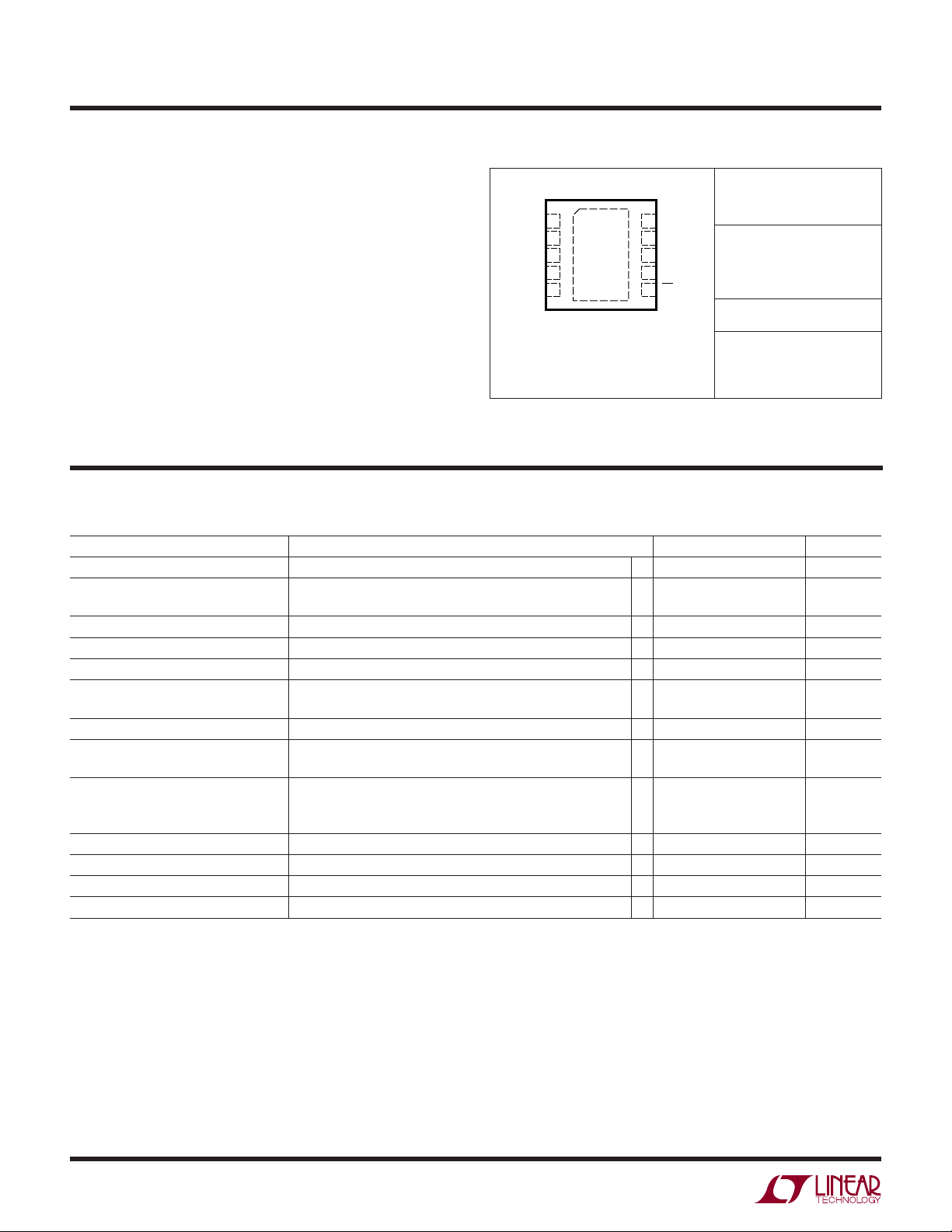
PACKAGE/ORDER I FOR ATIO
UU
W
WWWU
ABSOLUTE AXI U RATI GS
(Notes 1, 2)
Supply Voltage (VCC) to GND...................... – 0.3V to 6V
Analog Input Voltage to GND ....... –0.3V to (V
+ 0.3V)
CC
Reference Input Voltage to GND .. –0.3V to (VCC + 0.3V)
Digital Input Voltage to GND ........ –0.3V to (V
Digital Output Voltage to GND ..... –0.3V to (V
+ 0.3V)
CC
+ 0.3V)
CC
Operating Temperature Range
LTC2480C ................................................... 0°C to 70°C
LTC2480I ................................................ –40°C to 85°C
Storage Temperature Range ................ –65°C to 125°C
SDI
V
CC
V
REF
IN
IN
10-LEAD (3mm × 3mm) PLASTIC DFN
Consult LTC Marketing for parts specified with wider operating temperature ranges.
*The temperature grade is identified by a label on the shipping container.
TOP VIEW
1
2
11
3
+
4
–
5
DD PACKAGE
T
= 125°C, θJA = 43°C/ W
JMAX
EXPOSED PAD (PIN 11) IS GND
MUST BE SOLDERED TO PCB
10
9
8
7
6
F
O
SCK
GND
SDO
CS
ORDER PART
NUMBER
LTC2480CDD
LTC2480IDD
DD PART MARKING*
LBJY
UW
ELECTRICAL CHARACTERISTICS ( OR AL SPEED)
over the full operating temperature range, otherwise specifications are TA = 25°C. (Notes 3, 4)
PARAMETER CONDITIONS MIN TYP MAX UNITS
Resolution (No Missing Codes) 0.1 ≤ V
Integral Nonlinearity 5V ≤ VCC ≤ 5.5V, V
2.7V ≤ VCC ≤ 5.5V, V
Offset Error 2.5V ≤ V
Offset Error Drift 2.5V ≤ V
Positive Full-Scale Error 2.5V ≤ V
Positive Full-Scale Error Drift 2.5V ≤ V
Negative Full-Scale Error 2.5V ≤ V
Negative Full-Scale Error Drift 2.5V ≤ V
Total Unadjusted Error 5V ≤ VCC ≤ 5.5V, V
5V ≤ VCC ≤ 5.5V, V
2.7V ≤ VCC ≤ 5.5V, V
Output Noise 5V ≤ VCC ≤ 5.5V, V
Internal PTAT Signal TA = 27°C 420 mV
Internal PTAT Temperature Coefficient 1.4 mV/°C
Programmable Gain ● 1 256
≤ VCC, –FS ≤ VIN ≤ +FS (Note 5) ● 16 Bits
REF
= 5V, V
REF
= 2.5V, V
REF
≤ VCC, GND ≤ IN+ = IN– ≤ VCC (Note 14) ● 0.5 2.5 µV
REF
≤ VCC, GND ≤ IN+ = IN– ≤ V
REF
≤ VCC, IN+ = 0.75V
REF
≤ VCC, IN+ = 0.75V
REF
≤ VCC, IN+ = 0.75V
REF
≤ VCC, IN+ = 0.75V
REF
= 2.5V, V
REF
= 5V, V
REF
= 2.5V, V
REF
= 5V, GND ≤ IN– = IN+ ≤ VCC (Note 13) 0.6 µV
REF
= 2.5V (Note 6) ● 2 10 ppm of V
IN(CM)
IN(CM)
= 1.25V (Note 6) 1 ppm of V
IN(CM)
CC
, IN– = 0.25V
REF
, IN– = 0.25V
REF
, IN– = 0.25V
REF
, IN– = 0.25V
REF
= 1.25V 15 ppm of V
IN(CM)
= 2.5V ppm of V
IN(CM)
REF
REF
REF
REF
= 1.25V ppm of V
The ● denotes specifications which apply
REF
REF
10 nV/°C
● 25 ppm of V
0.1 ppm of
● 25 ppm of V
0.1 ppm of
REF
/°C
V
REF
REF
/°C
V
REF
REF
REF
REF
RMS
2
2480f
LTC2480
ELECTRICAL CHARACTERISTICS (2x SPEED)
The ● denotes specifications which apply over the full
operating temperature range, otherwise specifications are TA = 25°C. (Notes 3, 4)
PARAMETER CONDITIONS MIN TYP MAX UNITS
Resolution (No Missing Codes) 0.1 ≤ V
Integral Nonlinearity 5V ≤ VCC ≤ 5.5V, V
2.7V ≤ VCC ≤ 5.5V, V
Offset Error 2.5V ≤ V
Offset Error Drift 2.5V ≤ V
Positive Full-Scale Error 2.5V ≤ V
Positive Full-Scale Error Drift 2.5V ≤ V
Negative Full-Scale Error 2.5V ≤ V
Negative Full-Scale Error Drift 2.5V ≤ V
Output Noise 5V ≤ VCC ≤ 5.5V, V
≤ VCC, –FS ≤ VIN ≤ +FS (Note 5) ● 16 Bits
REF
= 5V, V
REF
= 2.5V, V
REF
≤ VCC, GND ≤ IN+ = IN– ≤ VCC (Note 14) ● 0.5 2 mV
REF
≤ VCC, GND ≤ IN+ = IN– ≤ V
REF
≤ VCC, IN+ = 0.75V
REF
≤ VCC, IN+ = 0.75V
REF
≤ VCC, IN+ = 0.75V
REF
≤ VCC, IN+ = 0.75V
REF
= 5V, GND ≤ IN– = IN+ ≤ VCC (Note 13) 0.84 µV
REF
= 2.5V (Note 6) ● 2 10 ppm of V
IN(CM)
= 1.25V (Note 6) 1
IN(CM)
CC
, IN– = 0.25V
REF
, IN– = 0.25V
REF
, IN– = 0.25V
REF
, IN– = 0.25V
REF
REF
REF
REF
REF
100 nV/°C
● 25 ppm of V
0.1 ppm of
● 25 ppm of V
0.1 ppm of
REF
REF
/°C
V
REF
REF
/°C
V
REF
RMS
Programmable Gain (Note 15) ● 1 128
U
CO VERTER CHARACTERISTICS
temperature range, otherwise specifications are at TA = 25°C. (Notes 3, 4)
PARAMETER CONDITIONS MIN TYP MAX UNITS
Input Common Mode Rejection DC 2.5V ≤ V
Input Common Mode Rejection 2.5V ≤ V
50Hz ±2%
Input Common Mode Rejection 2.5V ≤ V
60Hz ±2%
Input Normal Mode Rejection 2.5V ≤ V
50Hz ±2%
Input Normal Mode Rejection 2.5V ≤ V
60Hz ±2%
Input Normal Mode Rejection 2.5V ≤ V
50Hz/60Hz ±2%
Reference Common Mode 2.5V ≤ V
Rejection DC
Power Supply Rejection DC V
Power Supply Rejection, 50Hz ± 2% V
Power Supply Rejection, 60Hz ± 2% V
REF
REF
REF
≤ VCC, GND ≤ IN– = IN+ ≤ V
REF
≤ VCC, GND ≤ IN– = IN+ ≤ V
REF
≤ VCC, GND ≤ IN– = IN+ ≤ V
REF
≤ VCC, GND ≤ IN– = IN+ ≤ V
REF
≤ VCC, GND ≤ IN– = IN+ ≤ V
REF
≤ VCC, GND ≤ IN– = IN+ ≤ V
REF
≤ VCC, GND ≤ IN– = IN+ ≤ V
REF
= 2.5V, IN– = IN+ = GND 120 dB
= 2.5V, IN– = IN+ = GND (Notes 7, 9) 120 dB
= 2.5V, IN– = IN+ = GND (Notes 8, 9) 120 dB
The ● denotes specifications which apply over the full operating
(Note 5) ● 140 dB
CC
(Note 5) ● 140 dB
CC
(Note 5) ● 140 dB
CC
(Notes 5, 7) ● 110 120 dB
CC
(Notes 5, 8) ● 110 120 dB
CC
(Notes 5, 9) ● 87 dB
CC
(Note 5) ● 120 140 dB
CC
UUU
A ALOG I PUT AUD REFERE CE
temperature range, otherwise specifications are at TA = 25°C. (Note 3)
SYMBOL PARAMETER CONDITIONS MIN TYP MAX UNITS
+
IN
–
IN
FS Full Scale of the Differential Input (IN+ – IN–) ● 0.5V
LSB Least Significant Bit of the Output Code ● FS/2
V
IN
V
REF
Absolute/Common Mode IN+ Voltage GND – 0.3V VCC + 0.3V V
Absolute/Common Mode IN– Voltage GND – 0.3V VCC + 0.3V V
Input Differential Voltage Range (IN+ – IN–) ● –FS +FS V
Reference Voltage Range ● 0.1 V
The ● denotes specifications which apply over the full operating
/GAIN V
REF
16
CC
2480f
3
V
LTC2480
UUU
A ALOG I PUT AUD REFERE CE
temperature range, otherwise specifications are at TA = 25°C. (Note 3)
SYMBOL PARAMETER CONDITIONS MIN TYP MAX UNITS
CS (IN+)IN
CS (IN–)IN
CS (V
)V
REF
I
(IN+)IN+ DC Leakage Current Sleep Mode, IN+ = GND ● –10 1 10 nA
DC_LEAK
I
(IN–)IN– DC Leakage Current Sleep Mode, IN– = GND ● –10 1 10 nA
DC_LEAK
I
DC_LEAK (VREF
+
Sampling Capacitance 11 pF
–
Sampling Capacitance 11 pF
Sampling Capacitance 11 pF
REF
)V
DC Leakage Current Sleep Mode, V
REF
The ● denotes specifications which apply over the full operating
REF
= V
CC
● –100 1 100 nA
UU
DIGITAL I PUTS A D DIGITAL OUTPUTS
operating temperature range, otherwise specifications are at T
SYMBOL PARAMETER CONDITIONS MIN TYP MAX UNITS
V
IH
V
IL
V
IH
V
IL
I
IN
I
IN
C
IN
C
IN
V
OH
V
OL
V
OH
V
OL
I
OZ
High Level Input Voltage 2.7V ≤ VCC ≤ 5.5V ● VCC – 0.5 V
, SDI
CS, F
O
Low Level Input Voltage 2.7V ≤ VCC ≤ 5.5V ● 0.5 V
, SDI
CS, F
O
High Level Input Voltage 2.7V ≤ VCC ≤ 5.5V (Note 10) ● VCC – 0.5 V
SCK
Low Level Input Voltage 2.7V ≤ VCC ≤ 5.5V (Note 10) ● 0.5 V
SCK
Digital Input Current 0V ≤ VIN ≤ V
, SDI
CS, F
O
Digital Input Current 0V ≤ VIN ≤ VCC (Note 10) ● –10 10 µA
SCK
Digital Input Capacitance 10 pF
CS, F
, SDI
O
Digital Input Capacitance 10 pF
SCK
High Level Output Voltage IO = –800µA ● VCC – 0.5 V
SDO
Low Level Output Voltage IO = 1.6mA ● 0.4 V
SDO
High Level Output Voltage IO = –800µA ● VCC – 0.5 V
SCK
Low Level Output Voltage IO = 1.6mA ● 0.4 V
SCK
Hi-Z Output Leakage ● –10 10 µA
SDO
= 25°C. (Note 3)
A
CC
The ● denotes specifications which apply over the full
● –10 10 µA
WU
POWER REQUIRE E TS
otherwise specifications are at TA = 25°C. (Note 3)
SYMBOL PARAMETER CONDITIONS MIN TYP MAX UNITS
V
CC
I
CC
Supply Voltage ● 2.7 5.5 V
Supply Current Conversion Mode (Note 12) ● 160 250 µA
The ● denotes specifications which apply over the full operating temperature range,
Sleep Mode (Note 12)
● 12 µA
2480f
4
LTC2480
WU
TI I G CHARACTERISTICS
range, otherwise specifications are at TA = 25°C. (Note 3)
SYMBOL PARAMETER CONDITIONS MIN TYP MAX UNITS
f
EOSC
t
HEO
t
LEO
t
CONV_1
t
CONV_2
f
ISCK
D
ISCK
f
ESCK
t
LESCK
t
HESCK
t
DOUT_ISCK
t
DOUT_ESCK
t
1
t
2
t
3
t
4
t
KQMAX
t
KQMIN
t
5
t
6
t
7
t
8
External Oscillator Frequency Range (Note 15) ● 10 4000 kHz
External Oscillator High Period ● 0.125 100 µs
External Oscillator Low Period ● 0.125 100 µs
Conversion Time for 1x Speed Mode 50Hz Mode ● 157.2 160.3 163.5 ms
Conversion Time for 2x Speed Mode 50Hz Mode ● 78.7 80.3 81.9 ms
Internal SCK Frequency Internal Oscillator (Note 10) 38.4 kHz
Internal SCK Duty Cycle (Note 10) ● 45 55 %
External SCK Frequency Range (Note 10) ● 4000 kHz
External SCK Low Period (Note 10) ● 125 ns
External SCK High Period (Note 10) ● 125 ns
Internal SCK 24-Bit Data Output Time Internal Oscillator (Notes 10, 12) ● 0.61 0.625 0.64 ms
External SCK 24-Bit Data Output Time (Note 10) ● 24/f
CS↓ to SDO Low ● 0 200 ns
CS↑ to SDO High Z ● 0 200 ns
CS↓ to SCK↓ Internal SCK Mode ● 0 200 ns
CS↓ to SCK↑ External SCK Mode ● 50 ns
SCK↓ to SDO Valid ● 200 ns
SDO Hold After SCK↓ (Note 5) ● 15 ns
SCK Set-Up Before CS↓ ● 50 ns
SCK Hold After CS↓ ● 50 ns
SDI Setup Before SCK↑ (Note 5) ● 100 ns
SDI Hold After SCK↑ (Note 5) ● 100 ns
The ● denotes specifications which apply over the full operating temperature
60Hz Mode
Simultaneous 50Hz/60Hz Mode
External Oscillator
60Hz Mode
Simultaneous 50Hz/60Hz Mode
External Oscillator
External Oscillator (Notes 10, 11) f
External Oscillator (Notes 10, 11)
● 131.0 133.6 136.3 ms
● 144.1 146.9 149.9 ms
● 41036/f
● 65.6 66.9 68.2 ms
● 72.2 73.6 75.1 ms
● 20556/f
● 192/f
(in kHz) ms
EOSC
(in kHz) ms
EOSC
/8 kHz
EOSC
(in kHz) ms
EOSC
(in kHz) ms
ESCK
Note 1: Absolute Maximum Ratings are those values beyond which the life
of the device may be impaired.
Note 2: All voltage values are with respect to GND.
Note 3: VCC = 2.7V to 5.5V unless otherwise specified.
V
= V
REFCM
/2, FS = 0.5V
REF
VIN = IN+ – IN–, V
IN(CM)
/GAIN
REF
= (IN+ + IN–)/2
Note 4: Use internal conversion clock or external conversion clock source
with f
= 307.2kHz unless otherwise specified.
EOSC
Note 5: Guaranteed by design, not subject to test.
Note 6: Integral nonlinearity is defined as the deviation of a code from a
straight line passing through the actual endpoints of the transfer curve.
The deviation is measured from the center of the quantization band.
Note 7: 50Hz mode (internal oscillator) or f
= 256kHz ±2% (external
EOSC
oscillator).
Note 8: 60Hz mode (internal oscillator) or f
= 307.2kHz ±2% (external
EOSC
oscillator).
Note 9: Simultaneous 50Hz/60Hz mode (internal oscillator) or f
EOSC
=
280kHz ±2% (external oscillator).
Note 10: The SCK can be configured in external SCK mode or internal SCK
mode. In external SCK mode, the SCK pin is used as digital input and the
driving clock is f
output and the output clock signal during the data output is f
Note 11: The external oscillator is connected to the F
oscillator frequency, f
. In internal SCK mode, the SCK pin is used as digital
ESCK
, is expressed in kHz.
EOSC
pin. The external
O
ISCK
.
Note 12: The converter uses the internal oscillator.
Note 13: The output noise includes the contribution of the internal
calibration operations.
Note 14: Guaranteed by design and test correlation.
Note 15: Refer to Applications Information section for performance vs
data rate graphs.
2480f
5
LTC2480
INPUT VOLTAGE (V)
–12
TUE (ppm OF V
REF
)
–4
4
12
–8
0
8
–0.75 –0.25 0.25 0.75
2480 G03
1.25–1.25
VCC = 2.7V
V
REF
= 2.5V
V
IN(CM)
= 1.25V
F
O
= GND
85°C
25°C
–45°C
INPUT VOLTAGE (V)
–3
INL (ppm OF V
REF
)
–1
1
3
–2
0
2
–0.75 –0.25 0.25 0.75
2480 G06
1.25–1.25
VCC = 2.7V
V
REF
= 2.5V
V
IN(CM)
= 1.25V
F
O
= GND
–45°C, 25°C, 90°C
UW
TYPICAL PERFOR A CE CHARACTERISTICS
Integral Nonlinearity
(VCC = 5V, V
3
VCC = 5V
= 5V
V
REF
2
)
1
REF
0
–1
INL (ppm OF V
–2
–3
= 2.5V
V
IN(CM)
= GND
F
O
–45°C
85°C
–1.5 –0.5 0.5 1.5
INPUT VOLTAGE (V)
Total Unadjusted Error
(VCC = 5V, V
12
VCC = 5V
= 5V
V
REF
8
)
4
REF
0
V
IN(CM)
F
O
= 2.5V
= GND
REF
25°C
REF
= 5V)
= 5V)
25°C
85°C
–45°C
2480 G04
Integral Nonlinearity
(VCC = 5V, V
3
VCC = 5V
= 2.5V
V
REF
2
)
1
REF
0
–1
INL (ppm OF V
–2
2.5–2–2.5 –1 0 1 2
–3
= 1.25V
V
IN(CM)
= GND
F
O
–0.75 –0.25 0.25 0.75
= 2.5V)
REF
–45°C, 25°C, 90°C
INPUT VOLTAGE (V)
1.25–1.25
2480 G05
Total Unadjusted Error
(VCC = 5V, V
12
VCC = 5V
V
8
V
F
)
4
REF
0
REF
IN(CM)
= GND
O
= 5V
= 1.25V
= 2.5V)
REF
85°C
25°C
–45°C
Integral Nonlinearity
(VCC = 2.7V, V
= 2.5V)
REF
Total Unadjusted Error
(VCC = 2.7V, V
= 2.5V)
REF
–4
TUE (ppm OF V
–8
–12
–1.5 –0.5 0.5 1.5
INPUT VOLTAGE (V)
2.5–2–2.5 –1 0 1 2
2480 G01
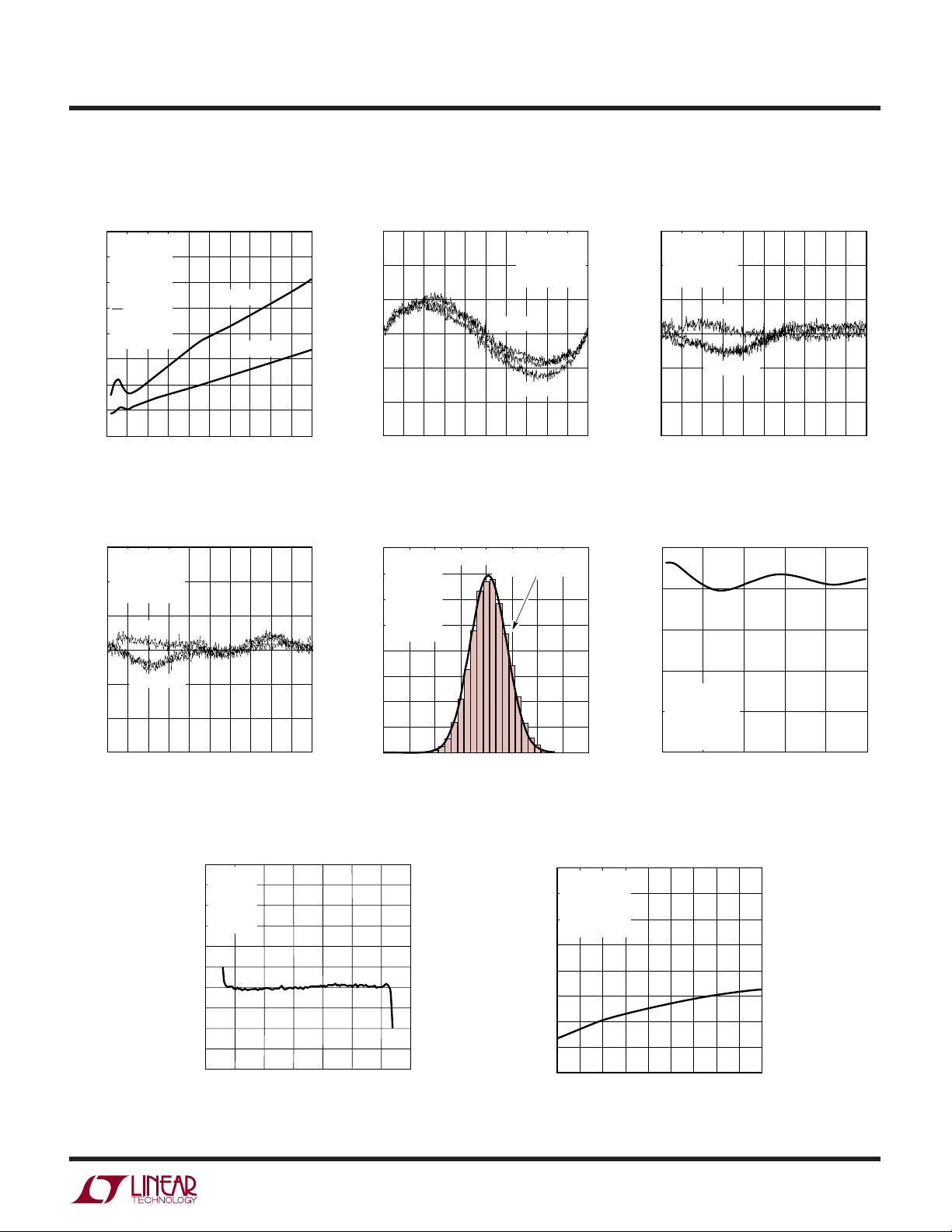
Noise Histogram (6.8sps) Long-Term ADC Readings
14
10,000 CONSECUTIVE
READINGS
12
= 5V
V
CC
= 5V
V
REF
= 0V
V
10
IN
GAIN = 256
= 25°C
T
A
8
6
4
NUMBER OF READINGS (%)
2
0
–3
–1.8 –0.6
–2.4 1.2
–1.2 0 1.8
OUTPUT READING (µV)
RMS = 0.60µV
AVERAGE = –0.69µV
0.6
2480 G07
–4
TUE (ppm OF V
–8
–12
–0.75 –0.25 0.25 0.75
INPUT VOLTAGE (V)
Noise Histogram (7.5sps)
14
10,000 CONSECUTIVE
READINGS
12
= 2.7V
V
CC
= 2.5V
V
REF
= 0V
V
10
IN
GAIN = 256
= 25°C
T
A
8
6
4
NUMBER OF READINGS (%)
2
0
–3
–1.8 –0.6
–2.4 1.2
–1.2 0 1.8
OUTPUT READING (µV)
2480 G02
RMS = 0.59µV
AVERAGE = –0.19µV
0.6
2480 G08
1.25–1.25
5
–1
ADC READING (µV)
–2
–3
–4
–5
VCC = 5V, V
GAIN = 256, T
4
3
2
1
0
0
= 5V, VIN = 0V, V
REF
= 25°C, RMS NOISE = 0.60µV
A
10
20
TIME (HOURS)
30 40
IN(CM)
= 2.5V
50
60
2480 G09
6
2480f
UW
V
REF
(V)
0
–0.3
OFFSET ERROR (ppm OF V
REF
)
–0.2
–0.1
0
0.1
0.2
0.3
1234
2480 G18
5
VCC = 5V
REF
–
= GND
V
IN
= 0V
V
IN(CM)
= GND
GAIN = 256
T
A
= 25°C
TYPICAL PERFOR A CE CHARACTERISTICS
RMS Noise
vs Input Differential Voltage RMS Noise vs V
)
REF
1.0
0.9
0.8
VCC = 5V
= 5V
V
REF
GAIN = 256
= 2.5V
V
IN(CM)
= 25°C
T
A
1.0
0.9
0.8
VCC = 5V
= 5V
V
REF
= 0V
V
IN
V
IN(CM)
GAIN = 256
= 25°C
T
A
= GND
IN(CM)
LTC2480
RMS Noise vs Temperature (TA)
1.0
VCC = 5V
= 5V
V
REF
0.9
= 0V
V
IN
= GND
V
IN(CM)
GAIN = 256
0.8
0.7
0.6
RMS NOISE (ppm OF V
0.5
0.4
–1.5 –0.5 0.5 1.5
INPUT DIFFERENTIAL VOLTAGE (V)
RMS Noise vs V
1.0
V
= 2.5V
REF
= 0V
V
IN
= GND
V
0.9
IN(CM)
GAIN = 256
= 25°C
T
A
0.8
0.7
RMS NOISE (µV)
0.6
0.5
0.4
2.7
3.1 3.5
CC
4.3 5.1 5.5
3.9 4.7
VCC (V)
2480 G10
2480 G13
0.7
RMS NOISE (µV)
0.6
0.5
2.5–2–2.5 –1 0 1 2
0.4
–1
01
RMS Noise vs V
1.0
VCC = 5V
= 0V
V
IN
0.9
V
IN(CM)
GAIN = 256
= 25°C
T
A
0.8
0.7
RMS NOISE (µV)
0.6
0.5
0.4
0
356
24
V
(V)
IN(CM)
2480 G11
REF
= GND
1234
V
(V)
REF
2480 G14
5
0.7
RMS NOISE (µV)
0.6
0.5
0.4
–45
–30 –15 15
0 304560
TEMPERATURE (°C)
Offset Error vs V
0.3
VCC = 5V
= 5V
V
REF
)
REF
–0.1
OFFSET ERROR (ppm OF V
–0.3
0.2
0.1
–0.2
V
GAIN = 256
T
0
–1
= 0V
IN
= 25°C
A
01
75 90
2480 G12
IN(CM)
356
24
V
(V)
IN(CM)
2480 G15
Offset Error vs Temperature
0.3
VCC = 5V
V
0.2
V
)
V
REF
F
0.1
0
–0.1
OFFSET ERROR (ppm OF V
–0.2
–0.3
–45
= 5V
REF
= 0V
IN
= GND
IN(CM)
= GND
O
–30 0
–15
30 90
45
15
TEMPERATURE (°C)
Offset Error vs V
0.3
REF+ = 2.5V
–
= GND
REF
)
REF
OFFSET ERROR (ppm OF V
60
75
2480 G16
0.2
0.1
–0.1
–0.2
–0.3
V
V
GAIN = 256
T
0
2.7
= 0V
IN
IN(CM)
= 25°C
A
3.1 3.5
= GND
CC
4.3 5.1 5.5
3.9 4.7
VCC (V)
2480 G17
Offset Error vs V
REF
2480f
7
LTC2480
TEMPERATURE (°C)
–45 –30
300
FREQUENCY (kHz)
304
310
–15
30
45
2480 G26
302
308
306
150
60 75
90
VCC = 4.1V
V
REF
= 2.5V
V
IN
= 0V
V
IN(CM)
= GND
F
O
= GND
TEMPERATURE (°C)
–45
0
SLEEP MODE CURRENT (µA)
0.2
0.6
0.8
1.0
2.0
1.4
–15
15
30 90
2480 G32
0.4
1.6
1.8
1.2
–30 0
45
60
75
VCC = 5V
VCC = 2.7V
FO = GND
CS = V
CC
SCK = NC
SDO = NC
SDI = GND
UW
TYPICAL PERFOR A CE CHARACTERISTICS
Temperature Sensor
vs Temperature
0.40
VCC = 5V
= 1.4V
V
REF
= GND
F
O
0.35
(V)
REF
0.30
/V
PTAT
V
0.25
0.20
–60
30090–30 60
TEMPERATURE (°C)
On-Chip Oscillator Frequency
vs V
CC
310
308
306
V
REF
V
IN
V
IN(CM)
F
O
= 2.5V
= 0V
= GND
2480 G24
= GND
120
Temperature Sensor Error
vs Temperature
5
VCC = 5V
4
= GND
F
O
3
2
1
0
–1
–2
TEMPERATURE ERROR (°C)
–3
–4
–5
–30
–60
0
TEMPERATURE (°C)
PSRR vs Frequency at V
0
VCC = 4.1V DC
= 2.5V
V
REF
–20
+
= GND
IN
–
= GND
IN
–40
= GND
F
O
= 25°C
T
A
–60
On-Chip Oscillator Frequency
vs Temperature
V
= 1.4V
REF
30
60
90
120
2480 G25
CC
PSRR vs Frequency at V
0
VCC = 4.1V DC ±1.4V
= 2.5V
V
REF
–20
+
= GND
IN
–
= GND
IN
–40
= GND
F
O
= 25°C
T
A
–60
CC
FREQUENCY (kHz)
REJECTION (dB)
8
–100
–120
–140
304
302
300
2.5
3.5 4.0 4.5
3.0
VCC (V)
PSRR vs Frequency at V
0
VCC = 4.1V DC ±0.7V
= 2.5V
V
REF
–20
+
= GND
IN
–
= GND
IN
–40
= GND
F
O
= 25°C
T
A
–60
–80
30600
30650 30700 30800
FREQUENCY AT VCC (Hz)
CC
30750
5.0 5.5
2480 G27
2480 G30
–80
REJECTION (dB)
–100
–120
–140
1
10 100
FREQUENCY AT VCC (Hz)
Conversion Current
vs Temperature
200
FO = GND
CS = GND
SCK = NC
180
SDO = NC
SDI = GND
160
140
CONVERSION CURRENT (µA)
120
100
–30 0
–15
–45
10k 1M
1k 100k
VCC = 5V
VCC = 2.7V
30 90
45
15
TEMPERATURE (°C)
–80
REJECTION (dB)
–100
–120
2480 G28
–140
100
120 160
140
0
60
80
40
20
FREQUENCY AT VCC (Hz)
180
220200
2480 G29
Sleep Mode Current
vs Temperature
60
75
2480 G31
2480f
UW
INPUT VOLTAGE (V)
–3
INL (ppm OF V
REF
)
–1
1
3
–2
0
2
–0.75 –0.25 0.25 0.75
2480 G35
1.25–1.25
VCC = 5V
V
REF
= 2.5V
V
IN(CM)
= 1.25V
F
O
= GND
90°C
–45°C, 25°C
TYPICAL PERFOR A CE CHARACTERISTICS
LTC2480
Conversion Current
vs Output Data Rate
500
V
= V
REF
CC
IN+ = GND
450
–
= GND
IN
SCK = NC
400
SDO = NC
SDI = GND
350
CS GND
= EXT OSC
F
O
300
= 25°C
T
A
250
SUPPLY CURRENT (µA)
200
150
100
0
20 40 60 1007010 30 50 90
OUTPUT DATA RATE (READINGS/SEC)
VCC = 5V
Integral Nonlinearity (2x Speed
Mode; VCC = 2.7V, V
3
VCC = 2.7V
= 2.5V
V
REF
2
)
1
REF
0
–1
INL (ppm OF V
–2
–3
= 1.25V
V
IN(CM)
= GND
F
O
90°C
–45°C, 25°C
–0.75 –0.25 0.25 0.75
INPUT VOLTAGE (V)
REF
VCC = 3V
80
= 2.5V)
2480 G33
2480 G36
Integral Nonlinearity (2x Speed
Mode; V
3
2
)
1
REF
0
–1
INL (ppm OF V
–2
–3
= 5V, V
CC
–1.5 –0.5 0.5 1.5
INPUT VOLTAGE (V)
= 5V)
REF
VCC = 5V
V
REF
V
IN(CM)
F
O
25°C, 90°C
–45°C
= 5V
= GND
= 2.5V
2.5–2–2.5 –1 0 1 2
2480 G34
Noise Histogram
(2x Speed Mode)
16
10,000 CONSECUTIVE
READINGS
14
= 5V
V
CC
= 5V
V
REF
12
= 0V
V
IN
GAIN = 256
10
= 25°C
T
A
8
6
4
NUMBER OF READINGS (%)
2
1.25–1.25
0
179
181.4 183.8 188.6
OUTPUT READING (µV)
RMS = 0.86µV
AVERAGE = 0.184mV
186.2
2480 G37
Integral Nonlinearity (2x Speed
Mode; V
RMS Noise vs V
= 5V, V
CC
REF
REF
(2x Speed Mode)
1.0
0.8
0.6
0.4
RMS NOISE (µV)
VCC = 5V
= 0V
V
IN
0.2
0
0
V
IN(CM)
F
O
T
A
= GND
= 25°C
= GND
1
3
2
V
(V)
REF
= 2.5V)
4
5
2480 G38
200
198
196
194
192
190
188
186
OFFSET ERROR (µV)
184
182
180
–1
Offset Error vs V
(2x Speed Mode)
VCC = 5V
= 5V
V
REF
= 0V
V
IN
= GND
F
O
= 25°C
T
A
2
1
0
V
IN(CM)
IN(CM)
3
(V)
Offset Error vs Temperature
(2x Speed Mode)
240
VCC = 5V
= 5V
V
REF
230
= 0V
V
IN
= GND
V
IN(CM)
220
= GND
F
O
210
200
190
OFFSET ERROR (µV)
180
170
5
6
2480 G39
4
160
–30 90
–45
–15
15
30
0
TEMPERATURE (°C)
75
45
60
2480 G40
2480f
9
LTC2480
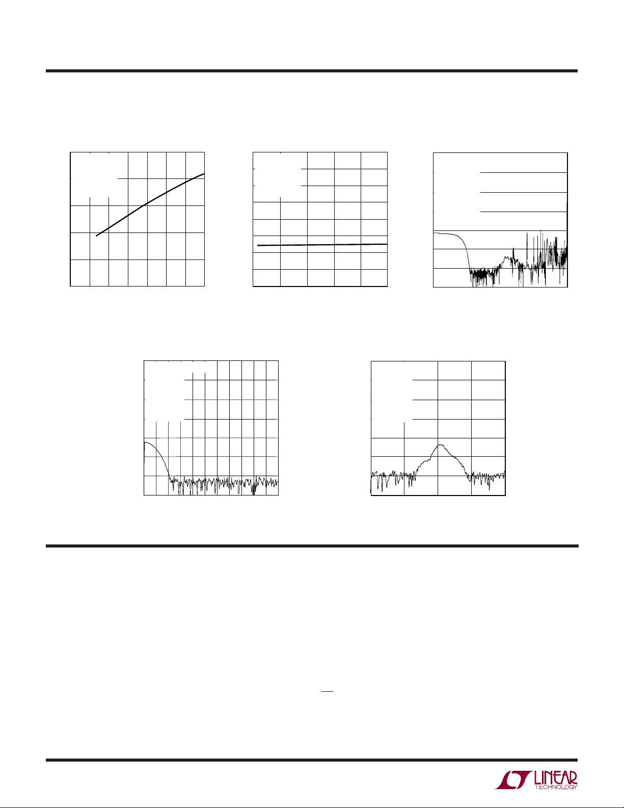
FREQUENCY AT VCC (Hz)
1
0
–20
–40
–60
–80
–100
–120
–140
1k 100k
2480 G43
10 100
10k 1M
REJECTION (dB)
VCC = 4.1V DC
REF
+
= 2.5V
REF
–
= GND
IN
+
= GND
IN
–
= GND
F
O
= GND
T
A
= 25°C
UW
TYPICAL PERFOR A CE CHARACTERISTICS
Offset Error vs V
(2x Speed Mode)
250
V
= 2.5V
REF
= 0V
V
IN
V
IN(CM)
200
= GND
F
O
= 25°C
T
A
150
100
OFFSET ERROR (µV)
50
0
2 2.5
= GND
3
CC
4
3.5
VCC (V)
4.5
5
2480 G41
PSRR vs Frequency at V
(2x Speed Mode)
0
VCC = 4.1V DC ±1.4V
+
= 2.5V
REF
–20
–
= GND
REF
+
= GND
IN
–
–40
= GND
IN
= GND
F
O
= 25°C
T
A
–60
5.5
Offset Error vs V
(2x Speed Mode)
240
VCC = 5V
= 0V
V
IN
230
V
IN(CM)
= GND
F
O
220
= 25°C
T
A
210
200
190
OFFSET ERROR (µV)
180
170
160
0
CC
REF
= GND
12 4
3
V
(V)
REF
2480 G42
PSRR vs Frequency at V
(2x Speed Mode)
0
VCC = 4.1V DC ±0.7V
REF
–20
REF
IN
–40
IN
F
O
T
A
–60
5
+
= 2.5V
–
= GND
+
= GND
–
= GND
= GND
= 25°C
PSRR vs Frequency at V
(2x Speed Mode)
CC
CC
PI FU CTIO S
SDI (Pin 1): Serial Data Input. This pin is used to select the
GAIN, line frequency rejection, input, temperature sensor
and 2x speed mode. Data is shifted into the SDI pin on the
rising edge of serial clock (SCK).
VCC (Pin 2): Positive Supply Voltage. Bypass to GND
(Pin 8) with a 1µF tantalum capacitor in parallel with 0.1µF
ceramic capacitor as close to the part as possible.
V
pin can have any value between 0.1V and VCC. The negative
reference input is GND (Pin 8).
–80
RREJECTION (dB)
–100
–120
–140
0
U
(Pin 3): Positive Reference Input. The voltage on this
REF
60
80
40
20
FREQUENCY AT VCC (Hz)
UU
100
120 160
140
180
220200
2480 G44
–80
REJECTION (dB)
–100
–120
–140
30600
30650 30700 30800
FREQUENCY AT VCC (Hz)
30750
2480 G45
IN+ (Pin 4), IN– (Pin 5): Differential Analog Inputs. The
voltage on these pins can have any value between GND –
0.3V and VCC + 0.3V. Within these limits the converter
bipolar input range (VIN = IN+ – IN–) extends from –0.5 •
V
/GAIN to 0.5 • V
REF
/GAIN. Outside this input range the
REF
converter produces unique overrange and underrange
output codes.
CS (Pin 6): Active LOW Chip Select. A LOW on this pin
enables the digital input/output and wakes up the ADC.
Following each conversion the ADC automatically enters
the Sleep mode and remains in this low power state as long
2480f
10
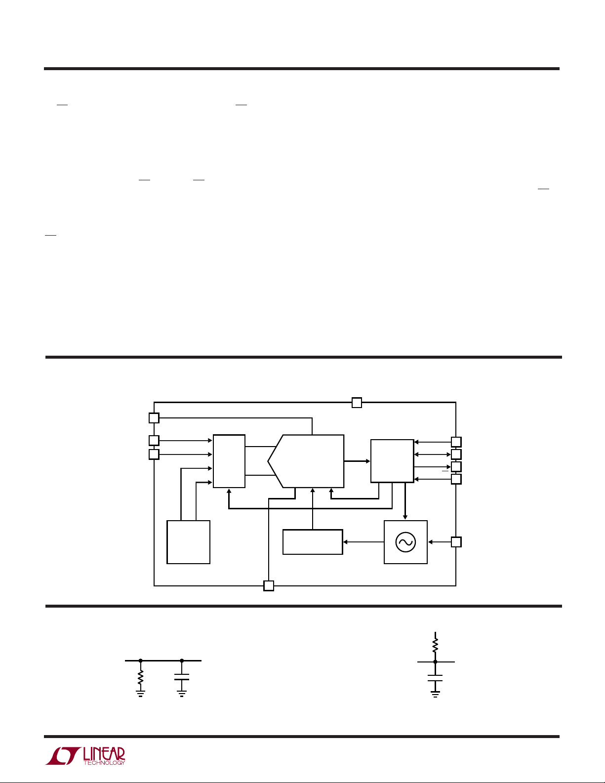
LTC2480
U
UU
PI FU CTIO S
as CS is HIGH. A LOW-to-HIGH transition on CS during the
Data Output transfer aborts the data transfer and starts a
new conversion.
SDO (Pin 7): Three-State Digital Output. During the Data
Output period, this pin is used as the serial data output.
When the chip select CS is HIGH (CS = V
is in a high impedance state. During the Conversion and
Sleep periods, this pin is used as the conversion status
output. The conversion status can be observed by pulling
CS LOW.
GND (Pin 8): Ground. Shared pin for analog ground,
digital ground and reference ground. Should be connected
directly to a ground plane through a minimum impedance.
SCK (Pin 9): Bidirectional Digital Clock Pin. In Internal
Serial Clock Operation mode, SCK is used as the digital
output for the internal serial interface clock during the Data
), the SDO pin
CC
Input/Output period. In External Serial Clock Operation
mode, SCK is used as the digital input for the external
serial interface clock during the Data Output period. A weak
internal pull-up is automatically activated in Internal Serial
Clock Operation mode. The Serial Clock Operation mode is
determined by the logic level applied to the SCK pin at
power up or during the most recent falling edge of CS.
F
(Pin 10): Frequency Control Pin. Digital input that
O
controls the conversion clock. When FO is connected to
GND the converter uses its internal oscillator running at
307.2kHz. The conversion clock may also be overridden
by driving the FO pin with an external clock in order to
change the output rate or the digital filter rejection null.
Exposed Pad (Pin 11): This pin is ground and should be
soldered to the PCB ground plane. For prototyping purposes, this pin may remain floating.
UU
W
FU CTIO AL BLOCK DIAGRA
V
REF
3
+
IN
4
–
IN
5
TEMP
SENSOR
MUX
TEST CIRCUITS
SDO
1.69k
C
LOAD
= 20pF
+
IN
–
IN
REF
AUTOCALIBRATION
GND
8
+
REF
3RD ORDER
∆Σ ADC
(1-256)
–
AND CONTROL
GAIN
2
V
CC
SDI
1
SCK
SERIAL
INTERFACE
INTERNAL
OSCILLATOR
SDO
9
SD0
7
CS
6
F
O
10
2480 FD
V
CC
1.69k
= 20pF
C
LOAD
Hi-Z TO V
VOL TO V
VOH TO Hi-Z
OH
OH
2480 TA02
Hi-Z TO V
VOH TO V
VOL TO Hi-Z
OL
OL
2480 TA03
2480f
11

LTC2480
WUW
TI I G DIAGRA S
CS
Timing Diagram Using Internal SCK
SDO
SCK
SDI
SDO
SCK
SDI
SLEEP
t
1
t
t
3
t
8
t
7
KQMIN
t
KQMAX
t
2
2480 TD1
CONVERSIONDATA IN/OUT
Timing Diagram Using External SCK
CS
SLEEP
t
1
t
5
t
6
t
4
t
8
t
7
t
KQMIN
t
KQMAX
t
2
2480 TD2
CONVERSIONDATA IN/OUT
WUUU
APPLICATIO S I FOR ATIO
CONVERTER OPERATION
Converter Operation Cycle
The LTC2480 is a low power, delta-sigma analog-todigital converter with an easy to use 4-wire serial interface
and automatic differential input current cancellation. Its
operation is made up of three states. The converter operating cycle begins with the conversion, followed by the low
power sleep state and ends with the data output (see
Figure 1). The 4-wire interface consists of serial data
output (SDO), serial clock (SCK), chip select (CS) and
serial data input (SDI).
Initially, the LTC2480 performs a conversion. Once the
conversion is complete, the device enters the sleep state.
12
CONVERT
SLEEP
FALSE
CS = LOW
AND
SCK
TRUE
DATA OUTPUT
CONFIGURATION INPUT
2480 F01
Figure 1. LTC2480 State Transition Diagram
2480f
 Loading...