

Ultra-Tiny, Differential,
16-Bit ΔΣ ADC With
FEATURES DESCRIPTION
■
±VCC Differential Input Range
■
16-Bit Resolution (Including Sign), No Missing
Codes
■
2LSB Offset Error
■
4LSB Full-Scale Error
■
60 Conversions Per Second
■
Single Conversion Settling Time for Multiplexed
Applications
■
Single-Cycle Operation with Auto Shutdown
■
800μA Supply Current
■
0.2μA Sleep Current
■
Internal Oscillator—No External Components
Required
■
2-Wire I2C Interface
■
Ultra-Tiny 8-Pin 3mm × 2mm DFN
and TSOT23 Packages
APPLICATIONS
■
System Monitoring
■
Environmental Monitoring
■
Direct Temperature Measurements
■
Instrumentation
■
Industrial Process Control
■
Data Acquisition
■
Embedded ADC Upgrades
, LT, LTC and LTM are registered trademarks of Linear Technology Corporation.
All other trademarks are the property of their respective owners.
Protected by U.S. Patents, including 6208279, 6411242, 7088280, 7164378.
The LTC®2453 is an ultra-tiny, fully differential, 16-bit,
analog-to-digital converter. The LTC2453 uses a single
2.7V to 5.5V supply and communicates through an I
interface. The ADC is available in an 8-pin, 3mm × 2mm
DFN package or 8-pin, 3mm × 3mm TSOT package. It
includes an integrated oscillator that does not require any
external components. It uses a delta-sigma modulator
as a converter core and has no latency for multiplexed
applications. The LTC2453 includes a proprietary input
sampling scheme that reduces the average input sampling current several orders of magnitude lower than
conventional delta-sigma converters. Additionally, due
to its architecture, there is negligible current leakage
between the input pins.
The LTC2453 can sample at 60 conversions per second,
and due to the very large oversampling ratio, has ex-tremely
relaxed antialiasing requirements. The LTC2453 includes
continuous internal offset and full-scale calibration algorithms which are transparent to the user, ensuring accuracy
over time and over the operating temperature range. The
converter has external REF
input voltage range can extend up to ±(V
Following a single conversion, the LTC2453 can automatically enter a sleep mode and reduce its power to less
than 0.2μA. If the user reads the ADC once a second, the
LTC2453 consumes an average of less than 50μW from
a 2.7V supply.
LTC2453
2
I
C Interface
+
and REF– pins and the differential
REF
+
– V
REF
–
).
2
C
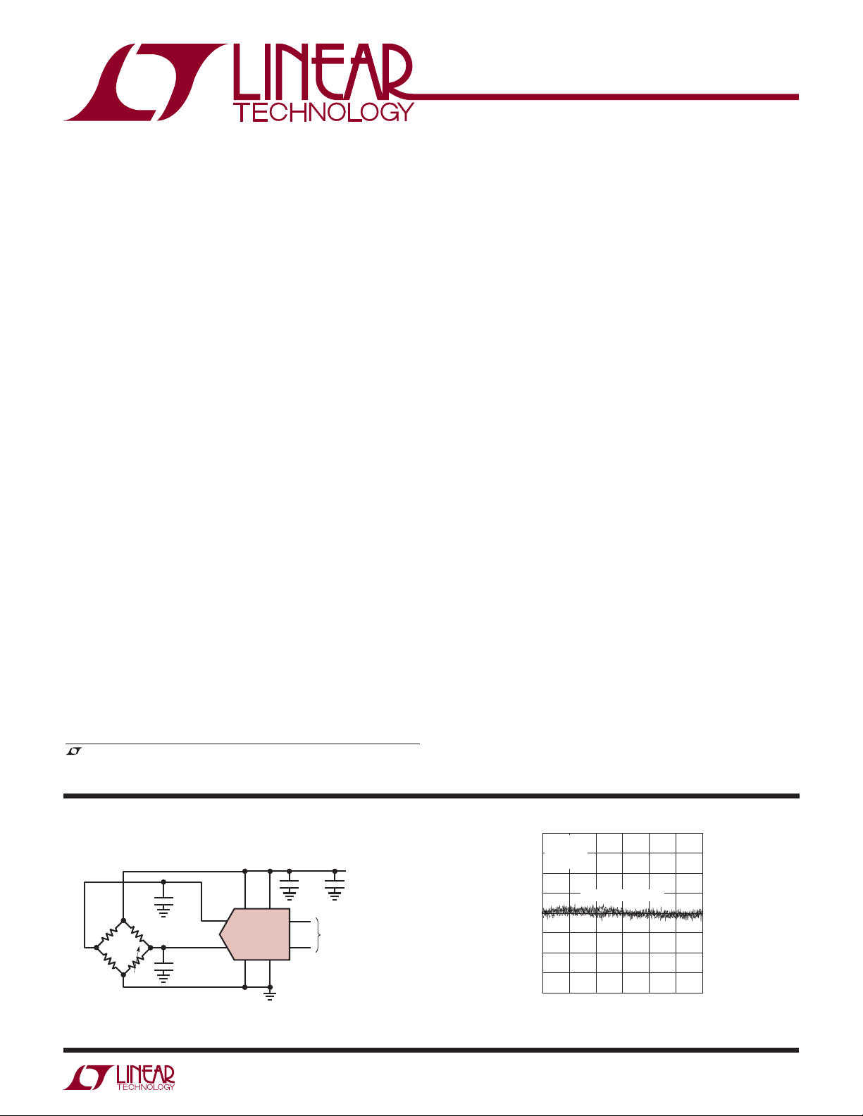
TYPICAL APPLICATION
IN
IN
REF+V
+
–
REF
LTC2453
–
CC
GND
2453 TA01
10k
10k
10k
R
0.1μF
0.1μF
0.1μF 10μF
SCL
2-WIRE I2C
SDA
INTERFACE
2.7V TO 5.5V
Integral Nonlinearity, VCC = 3V
2.0
VCC = 3V
+
= 3V
V
REF
1.5
–
V
= 0V
REF
1.0
0.5
0
INL (LSB)
–0.5
–1.0
–1.5
–2.0
–3
TA = –45°C, 25°C, 90°C
–2 –1 1
DIFFERENTIAL INPUT VOLTAGE (V)
0
2
3
2453fa
1
LTC2453
ABSOLUTE MAXIMUM RATINGS
(Notes 1, 2)
Supply Voltage (VCC) ................................... –0.3V to 6V
+
–
, V
Analog Input Voltage (V
Reference Voltage (V
REF
IN
+
, V
) .. –0.3V to (V
IN
–
) .. –0.3V to (V
REF
Digital Voltage (SDA, SCL) ............ –0.3V to (V
+ 0.3V)
CC
+ 0.3V)
CC
+ 0.3V)
CC
PIN CONFIGURATION
TOP VIEW
Storage Temperature Range ................... –65°C to 150°C
Operating Temperature Range
LTC2453C ................................................ 0°C to 70°C
LTC2453I.............................................. –40°C to 85°C
SDA
1GND
–
REF
2
+
REF
3
V
4
CC
8-LEAD (3mm × 2mm) PLASTIC DFN
C/I GRADE T
EXPOSED PAD (PIN 9) IS GND, MUST BE SOLDERED TO PCB
DDB PACKAGE
JMAX
8
SCL
7
9
= 125°C, θJA = 76°C/W
+
IN
6
–
IN
5
GND 1
REF¯ 2
REF
VCC4
C/I GRADE T
TOP VIEW
8 SDA
+
3
TS8 PACKAGE
8-LEAD PLASTIC TSOT-23
= 125°C, θJA = 140°C/W
JMAX
7 SCL
6 IN
5 IN¯
+
ORDER INFORMATION
Lead Free Finish
TAPE AND REEL (MINI) TAPE AND REEL PART MARKING* PACKAGE DESCRIPTION TEMPERATURE RANGE
LTC2453CDDB#TRMPBF LTC2453CDDB#TRPBF LDBQ
LTC2453IDDB#TRMPBF LTC2453IDDB#TRPBF LDBQ
LTC2453CTS8#TRMPBF LTC2453CTS8#TRPBF LTDCG 8-Lead Plastic TSOT-23 0°C to 70°C
LTC2453ITS8#TRMPBF LTC2453ITS8#TRPBF LTDCG 8-Lead Plastic TSOT-23 –40°C to 85°C
TRM = 500 pieces. *Temperature grades are identifi ed by a label on the shipping container.
Consult LTC Marketing for parts specifi ed with wider operating temperature ranges.
Consult LTC Marketing for information on lead based fi nish parts.
For more information on lead free part marking, go to: http://www.linear.com/leadfree/
For more information on tape and reel specifi cations, go to: http://www.linear.com/tapeandreel/
8-Lead Plastic (3mm × 2mm) DFN
8-Lead Plastic (3mm × 2mm) DFN
0°C to 70°C
–40°C to 85°C
ELECTRICAL CHARACTERISTICS
The l denotes the specifi cations which apply over the full operating
temperature range, otherwise specifi cations are at TA = 25°C. (Note 2)
PARAMETER CONDITIONS MIN TYP MAX UNITS
l
Resolution (No Missing Codes) (Note 3)
Integral Nonlinearity (Note 4)
Offset Error
Offset Error Drift 0.02 LSB/°C
Gain Error
Gain Error Drift 0.02 LSB/°C
Transition Noise 1.4 μV
Power Supply Rejection DC 80 dB
16 Bits
l
l
l
210 LSB
210 LSB
0.01 0.02 % of FS
RMS
2453fa
2

LTC2453
The l denotes the specifi cations which apply over the full
ANALOG INPUTS AND REFERENCES
operating temperature range, otherwise specifi cations are at T
SYMBOL PARAMETER CONDITIONS MIN TYP MAX UNITS
+
V
IN
–
V
IN
+
V
REF
–
V
REF
+
, V
V
OR
UR
–
, V
V
OR
UR
C
IN
I
DC_LEAK(IN+)
+
–
Positive Input Voltage Range
Negative Input Voltage Range
Positive Reference Voltage Range V
Negative Reference Voltage Range V
Overrange/Underrange Voltage, IN
+
V
Overrange/Underrange Voltage, IN– V
IN+, IN– Sampling Capacitance 0.35 pF
IN+ DC Leakage Current VIN = GND (Note 8)
V
I
DC_LEAK(IN–)
IN– DC Leakage Current VIN = GND (Note 8)
V
I
DC_LEAK(REF+, REF–)
I
CONV
POWER REQUIREMENTS
The l denotes the specifi cations which apply over the full operating temperature
REF+, REF– DC Leakage Current V
Input Sampling Current (Note 5) 50 nA
range, otherwise specifi cations are at TA = 25°C.
= 25°C.
A
+
– V
REF
REF
+
– V
REF
REF
= 5V, V
REF
= 5V, V
REF
= V
(Note 8)
IN
CC
= V
(Note 8)
IN
CC
= 3V (Note 8)
REF
l
0V
l
0V
–
≥ 2.5V
–
≥ 2.5V
–
= 2.5V (See Figure 2) 8 LSB
IN
+
= 2.5V (See Figure 2) 8 LSB
IN
l
VCC – 2.5 V
l
0V
l
–10
l
–10
l
–10
l
–10
l
–10 1 10 nA
1
1
1
1
CC
CC
CC
– 2.5 V
CC
10
10
10
10
nA
nA
nA
nA
V
V
V
SYMBOL PARAMETER CONDITIONS MIN TYP MAX UNITS
V
CC
I
CC
Supply Voltage
Supply Current
Conversion
Sleep
I2C INPUTS AND OUTPUTS
The l denotes the specifi cations which apply over the full operating temperature
l
2.7 5.5 V
l
l
800
0.2
1200
0.6
μA
μA
range, otherwise specifi cations are at TA = 25°C. (Notes 2, 7)
SYMBOL PARAMETER CONDITIONS MIN TYP MAX UNITS
V
IH
V
IL
I
I
V
HYS
V
OL
I
IN
C
I
C
B
High Level Input Voltage
Low Level Input Voltage
Digital Input Current
Hysteresis of Schmidt Trigger Inputs (Note 3)
Low Level Output Voltage (SDA) I = 3mA
Input Leakage 0.1VCC ≤ VIN ≤ 0.9V
Capacitance for Each I/O Pin
Capacitance Load for Each Bus Line
CC
l
0.7V
CC
l
l
–10 10 μA
l
0.05V
CC
l
l
l
10 pF
l
0.3V
CC
0.4 V
1μA
400 pF
V
V
V
2453fa
3
LTC2453
2.0
I2C TIMING CHARACTERISTICS
The
temperature range, otherwise specifi cations are at T
= 25°C. (Notes 2, 7)
A
l denotes the specifi cations which apply over the full operating
SYMBOL PARAMETER CONDITIONS MIN TYP MAX UNITS
t
CONV
f
SCL
t
HD(SDA)
t
LOW
t
HIGH
t
SU(STA)
t
HD(DAT)
t
SU(DAT)
t
r
t
f
t
SU(STO)
t
BUF
t
OF
Conversion Time
SCL Clock Frequency
Hold Time (Repeated) START Condition
LOW Period of the SCL Pin
HIGH Period of the SCL Pin
Set-Up Time for a Repeated START Condition
Data Hold Time
Data Set-Up Time
Rise Time for SDA, SCL Signals (Note 6)
Fall Time for SDA, SCL Signals (Note 6)
Set-Up Time for STOP Condition
Bus Free Time Between a Stop and Start Condition
Output Fall Time V
IHMIN
to V
ILMAX
Bus Load CB 10pF to
l
l
l
l
l
l
l
l
l
l
l
l
l
13 16.6 23 ms
0 400 kHz
0.6
1.3
0.6
0.6
0 0.9
100 ns
20 + 0.1C
20 + 0.1C
B
B
0.6
1.3
20 + 0.1C
B
300 ns
300 ns
250 ns
400pF (Note 6)
t
SP
Input Spike Suppression
Note 1: Stresses beyond those listed under Absolute Maximum Ratings
may cause permanent damage to the device. Exposure to any Absolute
Maximum Rating condition for extended periods may affect device
reliability and lifetime.
Note 2. All voltage values are with respect to GND. V
= 2.7V to 5.5V
CC
unless otherwise specifi ed.
+
V
V
REF
IN
= V
= V
–
– V
REF
+
– V
IN
, V
REF
REFCM
–
, –V
IN
≤ VIN ≤ V
REF
= (V
REF
REF
; V
+
+ V
INCM
–
)/2, FS = V
REF
= (V
+
–
– V
REF
;
REF
+
–
+ V
IN
)/2.
IN
Note 4. Integral nonlinearity is defi ned as the deviation of a code from a
straight line passing through the actual endpoints of the transfer curve.
Guaranteed by design and test correlation.
Note 5. Input sampling current is the average input current drawn from
the input sampling network while the LTC2453 is converting.
Note 6. C
= capacitance of one bus line in pF.
B
Note 7. All values refer to V
Note 8. A positive current is fl owing into the DUT pin.
l
IH(MIN
) and V
IL(MAX)
levels.
50 ns
Note 3. Guaranteed by design, not subject to test.
μs
μs
μs
μs
μs
μs
μs
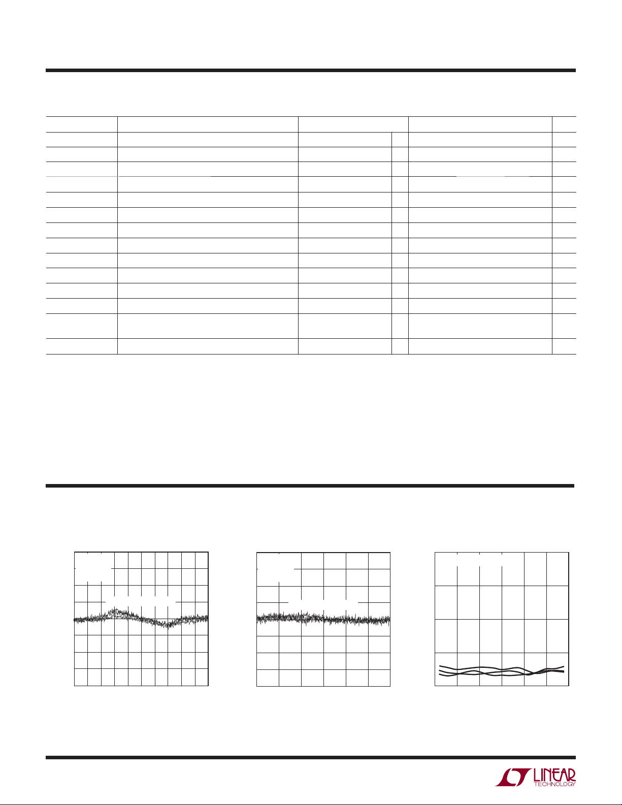
TYPICAL PERFORMANCE CHARACTERISTICS
Integral Nonlinearity, VCC = 5V
2.0
VCC = 5V
+
= 5V
V
1.5
REF
–
= 0V
V
REF
1.0
0.5
0
INL (LSB)
–0.5
–1.0
–1.5
–2.0
–5
TA = –45°C, 25°C, 90°C
–3 –1 1 52–4 –2 0 4
DIFFERENTIAL INPUT VOLTAGE (V)
3
2453 G01
Integral Nonlinearity, VCC = 3V Maximum INL vs Temperature
2.0
VCC = 3V
+
= 3V
V
REF
1.5
1.0
INL (LSB)
–0.5
–1.0
–1.5
–2.0
–
= 0V
V
REF
0.5
0
–3
TA = –45°C, 25°C, 90°C
–2 –1 1
DIFFERENTIAL INPUT VOLTAGE (V)
0
4
(TA = 25°C, unless otherwise noted)
VCC = V
1.5
1.0
INL (LSB)
0.5
0
3
2
2453 G02
–50
+
= 5V, 4.1V, 3V
REF
–25 0 25 50
TEMPERATURE (°C)
75 100
2453 G03
2453fa
LTC2453
8
TYPICAL PERFORMANCE CHARACTERISTICS
Offset Error vs Temperature Gain Error vs Temperature Transition Noise vs Temperature
5
4
3
VCC = V
2
1
OFFSET ERROR (LSB)
VCC = V
0
–1
–50
+
= 3V
REF
VCC = V
+
= 5V
REF
02550
–25
TEMPERATURE (°C)
REF
+
= 4.1V
Transition Noise vs Output Code
3.0
2.5
REF
REF
+
= 3V
+
= 5V
VCC = V
2.0
1.5
VCC = V
1.0
TRANSITION NOISE RMS (μV)
0.5
75 100
2453 G04
5
4
VCC = V
3
2
GAIN ERROR (LSB)
1
VCC = V
0
–50
+
= 3V
REF
VCC = V
+
= 5V
REF
02550
–25
TEMPERATURE (°C)
REF
+
= 4.1V
Conversion Mode Power Supply
Current vs Temperature
1200
60Hz OUTPUT SAMPLE RATE
1000
VCC = 5V
800
600
400
CONVERSION CURRENT (μA)
200
VCC = 3V
VCC = 4.1V
(TA = 25°C, unless otherwise noted)
3.0
2.5
2.0
VCC = 4.1V
VCC = 5V VCC = 3V
0
–50
–25
02550
TEMPERATURE (°C)
75 100
2453 G05
1.5
1.0
TRANSITION NOISE RMS (μV)
0.5
Sleep Mode Power Supply
Current vs Temperature
250
200
150
100
SLEEP CURRENT (nA)
50
VCC = 5V
VCC = 4.1V
VCC = 3V
75 100
2453 G06
0
–32768 3276
–16384 163840
OUTPUT CODE
Average Power Dissipation vs
Temperature, V
10000
1000
100
10
AVERAGE POWER DISSIPATION (μW)
1
–50
25Hz OUTPUT SAMPLE RATE
10Hz OUTPUT SAMPLE RATE
1Hz OUTPUT SAMPLE RATE
–25 0 25 50
= 3V
CC
TEMPERATURE (°C)
75 100
2453 G07
2453 G10
0
–50
02550
–25
TEMPERATURE (°C)
Power Supply Rejection vs
Frequency at V
0
VCC = 4.1V
+
= 2.7V
V
REF
–
= 0V
V
REF
–20
+
= 1V
V
IN
–
= 2V
V
IN
–40
–60
REJECTIOIN (dB)
–80
–100
110
CC
1k
100
FREQUENCY AT VCC (Hz)
10k
100k
75 100
2453 G08
10M
1M
2453 G11
0
–50
02550
–25
TEMPERATURE (°C)
Conversion Time vs Temperature
21
20
VCC = 3V
19
18
VCC = 5V
17
16
CONVERSION TIME (ms)
15
14
–50
–25 0
TEMPERATURE (°C)
VCC = 4.1V
25 75
75 100
2453 G09
50 100
2453 G12
2453fa
5
 Loading...