

advertisement
True Rail-to-Rail, High Input Impedance ADC Simplifi es
Precision Measurements –
Design Note 400
Mark Thoren
Introduction
High input impedance and a wide input range are two
highly desirable features in a precision analog-to-digital
converter, and the LTC
With just a few ex ternal components, the LTC2449 forms
an exceptional measurement system with ver y high input
impedance and an inpu t range that extends 30 0mV beyond
the supply rails.
A designer may trade off the LTC2449’s 200nV resolution
for faster conversion rates, but otherwise the LTC2449
requires few to no performance tradeoffs. It simultaneously achieves 1ppm linearity (Figure 2), 200nV input
resolution and a 5V input span. Ten fi lter oversample
ratios are ava ilable, providing data rate s from 6.8 samples
per second to 3500 samples per second. Normal mode
r e j e c t i o n o f 5 0 H z a n d 6 0 H z i s b e t t e r t h a n 8 7 d B i n t h e 6 . 8 s p s
mode. All DC specifi cations hold for all speeds —only the
resolution changes. Such persistent high performance
simplifi es the design of otherwise challenging applications, such as 6-digit voltmeters, sensor interfaces,
®
2449 delta-sigma ADC has both.
and industrial control. In addition, the LTC2449 digital
interface and timing are extremely simple, and the No
Latency architecture eliminates concerns about fi lter
settling when scanning multiple input channels.
Solving Common Issues
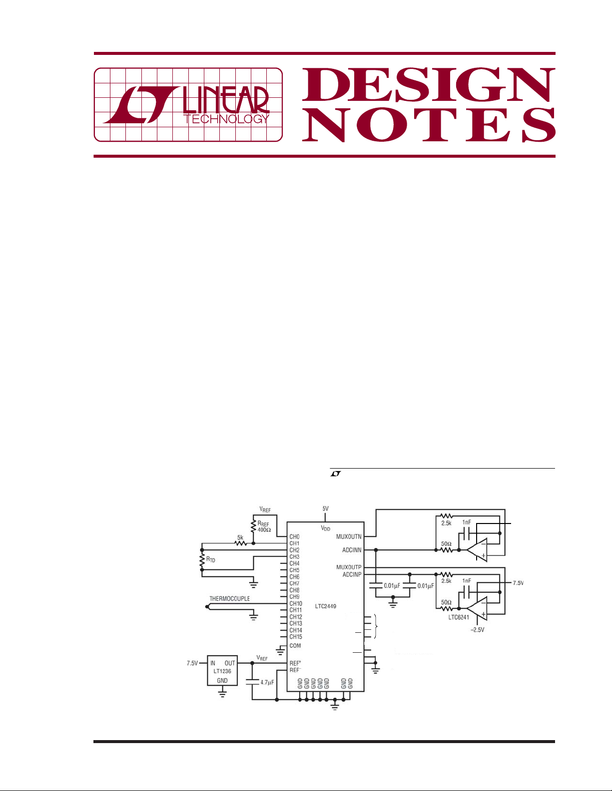
One unique feature of the LTC2449 is that the analog
inputs are routed to the MUXOUT pins, and an external
buffer isolates these signals from the switched capacitor ADC inputs (See Figure 1). The external buffer yields
high impedance through the multiplexer and back to
the analog inputs. This has a distinct advantage over
integrated buffers because the analog inputs are truly
rail-to-rail, and slightly beyond, with appropriate buffer
supply voltages.
The LTC6241 is a precision CMOS amplifi er with 1pA bias
current and impressive DC specifi cations: the maximum
offset is 125μV and the open loop gain is 1.6 million,
, LT, LTC and LTM are registered trademarks of Linear Technology Corporation.
All other trademarks are the property of their respective owners.
10/06/400
SDI
SCK
SPI INTERFACE
SDO
CS
BUSY
EXT
F
–
o
Figure 1. Temperature Sensing Application Example
7.5V
–2.5V
typical. While the offset is not important in this application because it is removed by the LTC2449’s multiplexer
switching technique, the high open loop gain ensures
that the 10ppm typical gain error of the LTC2449 does
not degrade. Figure 1 shows proper interfacing of the
LTC6241 to the LTC2449. The amplifi er’s 0.01μF capacitive
load and compensation network provides the LTC2449
with a charge reservoir to average the ADC’s sampling
current while the 2.5k feedback resistor maintains DC
accuracy.
The LTC6241 has a rail-to-rail output stage, and an
input common mode range from the negative supply to
1.5V lower than the positive supply. Since no rail-to-rail
amplifi er can actually pull its outputs to the rails, an
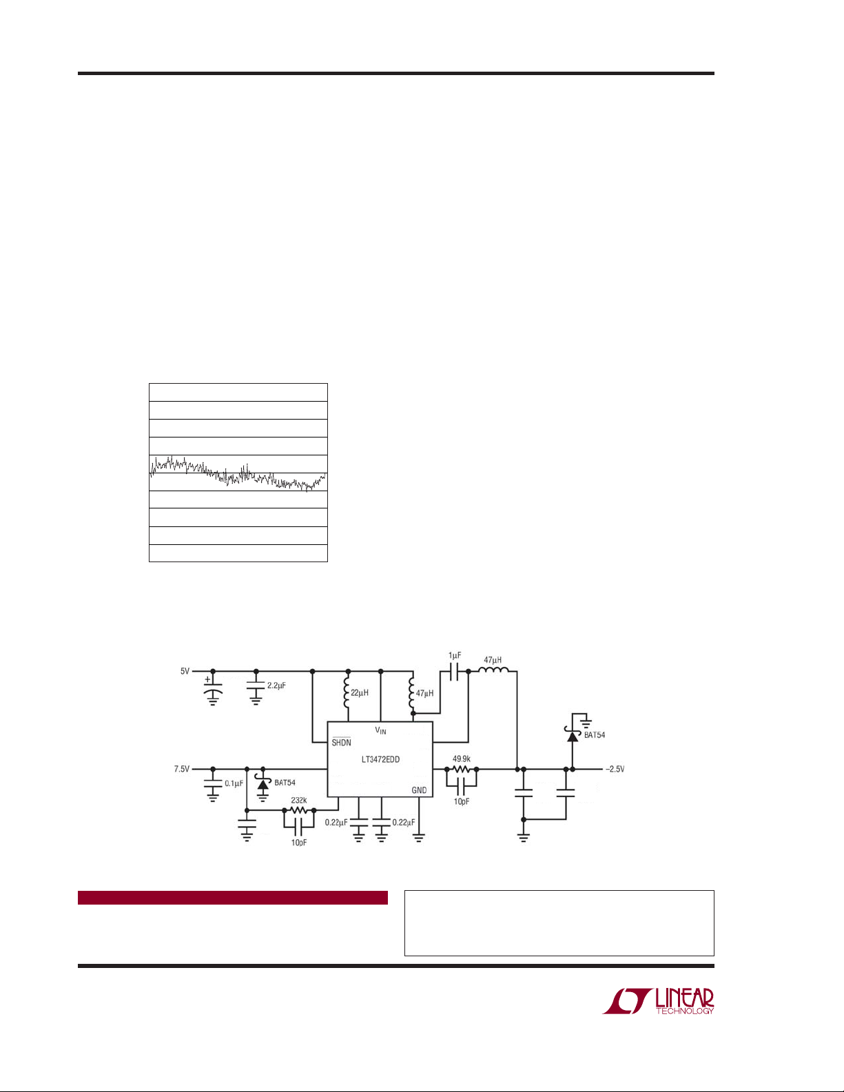
LT3472 boost/inverting regulator is used to create the
5
4
3
2
1
0
-1
-2
LINEARITY ERROR (ppm)
-3
-4
-5
-2.5 -2 -1.5 -1 -0.5 0
VIN (V)
Figure 2. LTC2449 Integral Non-Linearity
1 1.5 2 2.5
0.5
–2.5V and 7.5V op amp supplies from the 5V supply as
shown in Figure 3. This regulator can provide enough
current for several amplifi ers and other circuitry that re-
ally needs to swing to the rails. In addition, the LT3472’s
1.1MHz switching frequency is close to the middle of the
LTC 24 49 di gi t al fi l ter stopband. The center of the s topband
is 900kHz when using the internal conversion clock and
is independent of the selected speed mode.
Applications
T
he LTC2449 is commonly used with thermocouples
and RTDs as shown in Figure 1. Thermocouple outputs
produce very small changes (tens of microvolts per
degree C) and the output will be negative if the thermocouple is colder than the “cold juncti
on” connection
from the thermocouple to the copper traces on the PCB.
The RTD is measured by comparing the voltage across
the RTD to the voltage across a reference resistor. This
provides a very precise resistance comparison and it
does not require a precise current source. Grounding
the sensors as shown is a good fi rst line of defense for
reducing noise pickup; however, the ADC must accommodate input signals that are very close to or slightly
outside the supply rails. The LTC2449 handles these
signals perfectly.
Conclusion
The LTC2449 solves many of the problems that designers encounter when trying to apply delta-sigma ADCs
in demanding applications. High impedance, rail-to-rail
inputs and a very simple serial interface simplify both
hardware and software design.
47µF
47µF
Figure 3. Power Supply for Buffers
Data Sheet Download
www.linear.com
Linear Technology Corporation
1630 McCarthy Blvd., Milpitas, CA 95035-7417
(408) 432-1900
●
FAX: (408) 434-0507 ● www.linear.com
SWP
V
POS
FBP SSP SSN
SWN
DN
FBN
2.2µF 0.1µF
For applications help,
call (408) 432-1900, Ext. 2602
dn400f LT 1006 305K • PRINTED IN THE USA
© LINEAR TECHNOLOGY CORPORATION 2006
 Loading...