

查询LTC2445IUHF供应商
Selectable Multiple Reference Inputs
FEATURES
■
Five Selectable Differential Reference Inputs
■
Four Differential/Eight Single-Ended Inputs
■
4-Way MUX for Multiple Ratiometric
Measurements
■
Up to 8kHz Output Rate
■
Up to 4kHz Multiplexing Rate
■
Selectable Speed/Resolution:
2µV
200nV
Noise at 1.76kHz Output Rate
RMS
Noise at 13.8Hz Output Rate with
RMS
Simultaneous 50/60Hz Rejection
■
Guaranteed Modulator Stability and Lock-Up
Immunity for any Input and Reference Conditions
■
0.0005% INL, No Missing Codes
■
Autosleep Enables 20µA Operation at 6.9Hz
■
<5µV Offset (4.5V < VCC < 5.5V, – 40°C to 85°C)
■
Differential Input and Differential Reference with
GND to V
■
No Latency Mode, Each Conversion is Accurate Even
Common Mode Range
CC
After a New Channel is Selected
■
Internal Oscillator—No External Components
■
LTC2447 Includes MUXOUT/ADCIN for External
Buffering or Gain
■
Tiny QFN 5mm x 7mm Package
U
APPLICATIO S
■
Flow
■
Weight Scales
■
Pressure
■
Direct Temperature Measurement
■
Gas Chromatography
LTC2446/LTC2447
24-Bit High Speed
8-Channel ∆Σ ADCs with
U
DESCRIPTIO
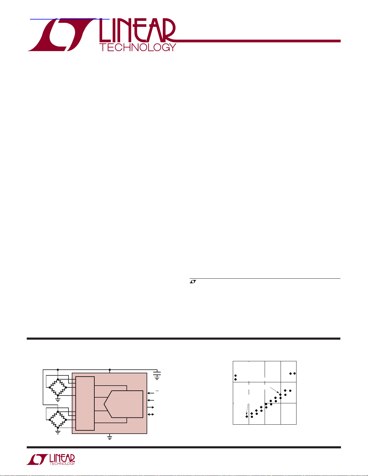
The LTC®2446/LTC2447 4-terminal switching enables
multiplexed ratiometric measurements. Four sets of selectable differential inputs coupled with four sets of differential reference inputs allow multiple RTDs, bridges and
other sensors to be digitized by a single converter. A fifth
differential reference input can be selected for any input
channel not requiring ratiometric measurements (thermocouples, voltages, current sense, etc.). The flexible
input multiplexer allows single-ended or differential inputs coupled with a slaved reference input or a universal
reference input.
A proprietary delta-sigma architecture results in absolute
accuracy (offset, full-scale, linearity) of 15ppm, noise as
low as 200nV
simple 4-wire interface, ten speed/resolution combinations can be selected. The first conversion following a
speed, resolution, channel change or reference change is
valid since there is no settling time between conversions,
enabling scan rates of up to 4kHz. Additionally, a 2x mode
can be selected for any speed-enabling output rates up to
8kHz with one cycle of latency.
, LTC and LT are registered trademarks of Linear Technology Corporation.
Protected by U.S. Patents, including 6140950, 6169506, 6208279, 6411242, 6639526
and speeds as high as 8kHz. Through a
RMS
TYPICAL APPLICATIO
Multiple Ratiometric Measurement System
V
CC
+
REF
+
IN
IN
REF
+
–
–
–
•
19-INPUT
•
4-OUTPUT
•
MUX
U
LTC2446
VARIABLE SPEED/
RESOLUTION 24-BIT
∆Σ ADC
24467 TA01
CS
SDI
SDO
SCK
LTC2446 Speed vs RMS Noise
100
VCC = 5V
= 5V
V
REF
+
–
= V
= 0V
V
IN
IN
2x SPEED MODE
NO LATENCY MODE
10
RMS NOISE (µV)
1
0.1
2.8µV AT 880Hz
280nV AT 6.9Hz
(50/60Hz REJECTION)
1
10 100
CONVERSION RATE (Hz)
1000 10000
24467 TA02
24467fa
1

LTC2446/LTC2447
WW
W
ABSOLUTE AXI U RATI GS
U
(Notes 1, 2)
Supply Voltage (VCC) to GND.......................–0.3V to 6V
Analog Input Pins Voltage
to GND .................................... – 0.3V to (V
+ 0.3V)
CC
Reference Input Pins Voltage
to GND .................................... – 0.3V to (V
Digital Input Voltage to GND ........ –0.3V to (V
+ 0.3V)
CC
+ 0.3V)
CC
UUW
PACKAGE/ORDER I FOR ATIO
TOP VIEW
SCK
SDOCSFOSDI
38 37 36 35 34 33 32
1GND
BUSY
2
EXT
3
GND
4
GND
5
GND
6
COM
7
CH0
8
CH1
9
–
V
10
REF01
+
V
11
REF01
CH2
12
13 14 15 16
–
CH3
REF23
V
38-LEAD (5mm × 7mm) PLASTIC QFN
UHF PACKAGE
T
= 125°C, θJA = 34°C/W
JMAX
EXPOSED PAD (PIN 39) IS GND
MUST BE SOLDERED TO PCB
+
V
REF23
39
CH4
GND
17 18 19
–
CH5
REF45
V
GND
+
REF45
V
31
GND
–
REFG
30
+
REFG
29
V
28
CC
NC
27
NC
26
NC
25
NC
24
+
V
23
REF67
–
22
V
REF67
21
CH7
20
CH6
Digital Output Voltage to GND ..... – 0.3V to (V
+ 0.3V)
CC
Operating Temperature Range
LTC2446C/LTC2447C .............................. 0°C to 70°C
LTC2446I/LTC2447I ........................... – 40°C to 85°C
Storage Temperature Range ................. –65°C to 125°C
TOP VIEW
SCK
SDOCSFOSDI
38 37 36 35 34 33 32
1GND
BUSY
2
EXT
3
GND
4
GND
5
GND
6
COM
7
CH0
8
CH1
9
–
V
10
REF01
+
V
11
REF01
CH2
12
13 14 15 16
_
CH3
REF23
V
38-LEAD (5mm × 7mm) PLASTIC QFN
UHF PACKAGE
T
= 125°C, θJA = 34°C/W
JMAX
EXPOSED PAD (PIN 39) IS GND
MUST BE SOLDERED TO PCB
+
VREF23
39
CH4
GND
17 18 19
–
CH5
REF45
V
+
GND
REF45
V
31
30
29
28
27
26
25
24
23
22
21
20
GND
–
REFG
+
REFG
V
CC
MUXOUTN
ADCINN
ADCINP
MUXOUTP
+
V
REF67
–
V
REF67
CH7
CH6
ORDER PART
NUMBER
LTC2446CUHF
LTC2446IUHF
QFN PART
MARKING*
2446
ORDER PART
NUMBER
LTC2447CUHF
LTC2447IUHF
QFN PART
MARKING*
2447
Order Options Tape and Reel: Add #TR Lead Free: Add #PBF Lead Free Tape and Reel: Add #TRPBF
Lead Free Part Marking: http://www.linear.com/leadfree/
*The temperature grade is identified by a label on the shipping container. Consult LTC Marketing for parts specified with wider operating temperature ranges.
24467fa
2
LTC2446/LTC2447
ELECTRICAL CHARACTERISTICS
temperature range, otherwise specifications are at T
The ● denotes specifications which apply over the full operating
= 25°C. (Notes 3, 4)
A
PARAMETER CONDITIONS MIN TYP MAX UNITS
Resolution (No Missing Codes) 0.1V ≤ V
Integral Nonlinearity VCC = 5V, REF+ = 5V, REF– = GND, V
REF+ = 2.5V, REF– = GND, V
Offset Error 2.5V ≤ REF+ ≤ VCC, REF– = GND,
GND ≤ IN
Offset Error Drift 2.5V ≤ REF+ ≤ VCC, REF– = GND, 20 nV/°C
GND ≤ IN
Positive Full-Scale Error REF+ = 5V, REF– = GND, IN+ = 3.75V, IN– = 1.25V
REF+ = 2.5V, REF– = GND, IN+ = 1.875V, IN– = 0.625V
Positive Full-Scale Error Drift 2.5V ≤ REF+ ≤ VCC, REF– = GND, 0.2 ppm of V
IN
+
Negative Full-Scale Error REF+ = 5V, REF– = GND, IN+ = 1.25V, IN– = 3.75V
REF+ = 2.5V, REF– = GND, IN+ = 0.625V, IN– = 1.875V
Negative Full-Scale Error Drift 2.5V ≤ REF+ ≤ VCC, REF– = GND, 0.2 ppm of V
IN
+
Total Unadjusted Error 5V ≤ VCC ≤ 5.5V, REF+ = 2.5V, REF– = GND, V
5V ≤ VCC ≤ 5.5V, REF+ = 5V, REF– = GND, V
REF+ = 2.5V, REF– = GND, V
Input Common Mode Rejection DC 2.5V ≤ REF+ ≤ VCC, REF– = GND, 120 dB
GND ≤ IN
≤ VCC, –0.5 • V
REF
+
= IN– ≤ VCC (Note 12)
+
= IN– ≤ V
CC
= 0.75REF+, IN– = 0.25 • REF
≤ VIN ≤ 0.5 • V
REF
= 1.25V, (Note 6) 3 ppm of V
INCM
+
= 0.25 • REF+, IN– = 0.75 • REF
= 1.25V, (Note 6) 15 ppm of V
INCM
–
= IN+ ≤ V
CC
= 2.5V, (Note 6)
INCM
+
INCM
, (Note 5)
REF
= 1.25V 15 ppm of V
INCM
●
24 Bits
●
●
●
●
●
●
5 15 ppm of V
2.5 5 µV
10 50 ppm of V
10 50 ppm of V
10 50 ppm of V
10 50 ppm of V
= 2.5V 15 ppm of V
REF
REF
REF
REF
REF
REF
/°C
REF
REF
/°C
REF
REF
REF
UUU
A ALOG I PUT AUD REFERE CE
temperature range, otherwise specifications are at T
SYMBOL PARAMETER CONDITIONS MIN TYP MAX UNITS
+
IN
–
IN
V
IN
+
REF
–
REF
V
REF
C
S(IN+)
C
S(IN–)
C
S(REF+)
C
S(REF–)
I
DC_LEAK(IN+, IN–,
REF+, REF–)
I
SAMPLE(IN+, IN–,
REF+, REF–)
t
OPEN
QIRR MUX Off Isolation VIN = 2V
Absolute/Common Mode IN+ Voltage
Absolute/Common Mode IN– Voltage
Input Differential Voltage Range
+
(IN
– IN–)
Absolute/Common Mode REF+ Voltage
Absolute/Common Mode REF– Voltage
Reference Differential Voltage Range
+
(REF
– REF–)
IN+ Sampling Capacitance 2 pF
IN– Sampling Capacitance 2 pF
REF+ Sampling Capacitance 2 pF
REF– Sampling Capacitance 2 pF
Leakage Current, Inputs and Reference CS = VCC, IN+ = GND, IN– = GND,
Average Input/Reference Current Varies, See Applications Section nA
During Sampling
MUX Break-Before-Make 50 ns
= 25°C. (Note 3)
A
REF+ = 5V, REF– = GND
The ● denotes specifications which apply over the full operating
●
GND – 0.3V VCC + 0.3V V
●
GND – 0.3V VCC + 0.3V V
●
–V
/2 V
REF
●
●
●
●
DC to 1.8MHz 120 dB
P-P
0.1 V
GND VCC – 0.1V V
0.1 V
–15 1 15 nA
/2 V
REF
CC
CC
V
V
24467fa
3
LTC2446/LTC2447
UU
DIGITAL I PUTS A D DIGITAL OUTPUTS
operating temperature range, otherwise specifications are at T
SYMBOL PARAMETER CONDITIONS MIN TYP MAX UNITS
V
IH
V
IL
V
IH
V
IL
I
IN
I
IN
C
IN
C
IN
V
OH
V
OL
V
OH
V
OL
I
OZ
High Level Input Voltage 4.5V ≤ VCC ≤ 5.5V
CS, F
O
Low Level Input Voltage 4.5V ≤ VCC ≤ 5.5V
CS, F
O
High Level Input Voltage 4.5V ≤ VCC ≤ 5.5V (Note 8)
SCK
Low Level Input Voltage 4.5V ≤ VCC ≤ 5.5V (Note 8)
SCK
Digital Input Current 0V ≤ VIN ≤ V
, EXT, SOI
CS, F
O
Digital Input Current 0V ≤ VIN ≤ VCC (Note 8)
SCK
Digital Input Capacitance 10 pF
CS, F
O
Digital Input Capacitance (Note 8) 10 pF
SCK
High Level Output Voltage IO = –800µA
SDO, BUSY
Low Level Output Voltage IO = 1.6mA
SDO, BUSY
High Level Output Voltage IO = –800µA (Note 9)
SCK
Low Level Output Voltage IO = 1.6mA (Note 9)
SCK
Hi-Z Output Leakage
SDO
= 25°C. (Note 3)
A
CC
The ● denotes specifications which apply over the full
●
●
●
●
●
●
●
●
●
●
●
2.5 V
0.8 V
2.5 V
0.8 V
–10 10 µA
–10 10 µA
VCC – 0.5V V
0.4V V
VCC – 0.5V V
0.4V V
–10 10 µA
WU
POWER REQUIRE E TS
otherwise specifications are at T
SYMBOL PARAMETER CONDITIONS MIN TYP MAX UNITS
V
CC
I
CC
Supply Voltage
Supply Current
Conversion Mode CS = 0V (Note 7)
Sleep Mode CS = V
= 25°C. (Note 3)
A
The ● denotes specifications which apply over the full operating temperature range,
(Note 7)
CC
●
●
●
4.5 5.5 V
811 mA
830 µA
UW
TI I G CHARACTERISTICS
range, otherwise specifications are at T
SYMBOL PARAMETER CONDITIONS MIN TYP MAX UNITS
f
EOSC
t
HEO
t
LEO
t
CONV
f
ISCK
External Oscillator Frequency Range
External Oscillator High Period
External Oscillator Low Period
Conversion Time OSR = 256
Internal SCK Frequency Internal Oscillator (Note 9)
= 25°C. (Note 3)
A
The ● denotes specifications which apply over the full operating temperature
●
●
●
●
OSR = 32768
External Oscillator (Notes 10, 13)
External Oscillator (Notes 9, 10) f
●
●
●
0.1 20 MHz
25 10000 ns
25 10000 ns
0.99 1.13 1.33 ms
126 145 170 ms
40 • OSR +170
f
(kHz)
EOSC
0.8 0.9 1 MHz
/10 Hz
EOSC
24467fa
ms
4
LTC2446/LTC2447
WU
TI I G CHARACTERISTICS
range, otherwise specifications are at T
SYMBOL PARAMETER CONDITIONS MIN TYP MAX UNITS
D
ISCK
f
ESCK
t
LESCK
t
HESCK
t
DOUT_ISCK
t
DOUT_ESCK
t
1
t
2
t
3
t
4
t
KQMAX
t
KQMIN
t
5
t
6
t
7
t
8
Note 1: Absolute Maximum Ratings are those values beyond which the life
of the device may be impaired.
Note 2: All voltage values are with respect to GND.
Note 3: V
= REF+ – REF–, V
V
REF
reference input, REF
= (IN+ + IN–)/2.
V
INCM
Note 4: F
= 10MHz unless otherwise specified.
f
EOSC
Note 5: Guaranteed by design, not subject to test.
Note 6: Integral nonlinearity is defined as the deviation of a code from a
straight line passing through the actual endpoints of the transfer curve.
The deviation is measured from the center of the quantization band.
Internal SCK Duty Cycle (Note 9)
External SCK Frequency Range (Note 8)
External SCK Low Period (Note 8)
External SCK High Period (Note 8)
Internal SCK 32-Bit Data Output Time Internal Oscillator (Notes 9, 11)
External SCK 32-Bit Data Output Time (Note 8)
CS ↓ to SDO Low Z (Note 12)
CS ↑ to SDO High Z (Note 12)
CS ↓ to SCK ↓ (Note 9) 5 µs
CS ↓ to SCK ↑ (Notes 8, 12)
SCK ↓ to SDO Valid
SDO Hold After SCK ↓ (Note 5)
SCK Setup Before CS ↓
SCK Hold After CS ↓
SDI Setup Before SCK ↑ (Note 5)
SDI Hold After SCK ↑ (Note 5)
= 4.5V to 5.5V unless otherwise specified.
CC
pin tied to GND or to external conversion clock source with
O
= (REF+ + REF–)/2; REF+ is the positive
REFCM
–
is the negative reference input; VIN = IN+ – IN–,
= 25°C. (Note 3)
A
The ● denotes specifications which apply over the full operating temperature
External Oscillator (Notes 9, 10)
Note 7: The converter uses the internal oscillator.
Note 8: The converter is in external SCK mode of operation such that the
SCK pin is used as a digital input. The frequency of the clock signal driving
SCK during the data output is f
Note 9: The converter is in internal SCK mode of operation such that the
SCK pin is used as a digital output. In this mode of operation, the SCK pin
has a total equivalent load capacitance of C
Note 10: The external oscillator is connected to the F
oscillator frequency, f
Note 11: The converter uses the internal oscillator. F
Note 12: Guaranteed by design and test correlation.
Note 13: There is an internal reset that adds an additional 1µs (typ) to the
conversion time.
●
●
●
●
●
●
●
●
●
●
●
●
●
●
●
●
EOSC
45 55 %
20 MHz
25 ns
25 ns
41.6 35.3 30.9 µs
320/f
EOSC
32/f
ESCK
025ns
025ns
25 ns
25 ns
15 ns
50 ns
50 ns
10 ns
10 ns
and is expressed in Hz.
ESCK
= 20pF.
LOAD
pin. The external
, is expressed in Hz.
O
= 0V.
O
s
s
U
UU
PI FU CTIO S
GND (Pins 1, 4, 5, 6, 31, 32, 33): Ground. Multiple
ground pins internally connected for optimum ground
current flow and VCC decoupling. Connect each one of
these pins to a common ground plane through a low
impedance connection. All seven pins must be connected
to ground for proper operation.
BUSY (Pin 2): Conversion in Progress Indicator. This pin
is HIGH while the conversion is in progress and goes LOW
indicating the conversion is complete and data is ready. It
remains LOW during the sleep and data output states. At
the conclusion of the data output state, it goes HIGH
indicating a new conversion has begun.
EXT (Pin 3): Internal/External SCK Selection Pin. This pin
is used to select internal or external SCK for outputting/
inputting data. If EXT is tied low, the device is in the
external SCK mode and data is shifted out of the device
under the control of a user applied serial clock. If EXT is
tied high, the internal serial clock mode is selected. The
device generates its own SCK signal and outputs this on
the SCK pin. A framing signal BUSY (Pin 2) goes low
indicating data is being output.
COM (Pin 7): The common negative input (IN
–
) for all
single ended multiplexer configurations. The voltage on
CH0-CH7 and COM pins can have any value between GND
24467fa
5

LTC2446/LTC2447
UUU
PI FU CTIO S
– 0.3V to V
inputs (IN
+
– IN–) from –0.5 • V
IN
+ 0.3V. Within these limits, the two selected
CC
+
and IN–) provide a bipolar input range (VIN =
to 0.5 • V
REF
. Outside this input
REF
range, the converter produces unique over-range and
under-range output codes.
CH0 to CH7 (Pins 8, 9, 12, 13, 16, 17, 20, 21): Analog
Inputs. May be programmed for Single-ended or Differential mode.
V
REF01
V
REF23
V
REF67
+
(Pin 11), V
–
(Pin 14), V
+
(Pin 23), V
REF67
–
(Pin 10) V
REF01
+
(Pin 19), V
REF45
–
(Pin 22): Differential Reference
REF23
REF45
+
(Pin 15),
–
(Pin 18),
Inputs. The voltage on these pins can be anywhere
between 0V and V
+
input (V
EF01
, V
the corresponding negative reference input (V
–
V
REF23
, V
REF45
as long as the positive reference
CC
REF23
–
, V
+
, V
REF67
+
, V
REF45
–
) by at least 100mV.
+
) is greater than
REF67
REF01
–
,
NC (Pins 24, 25, 26, 27): LTC2446 No Connect. These
pins can either be tied to ground or left floating.
MUXOUTP (Pin 24): LTC2447 Positive Input Channel
Multiplexer Output. Used to drive the input to an external
buffer/amplifier for the selected positive input signal (IN
+
).
ADCINP (Pin 25): LTC2447 Positive ADC Input. Tie to
output of buffer/amplifier driven by MUXOUTP.
ADCINN (Pin 26): LTC2447 Negative ADC Input. Tie to
output of buffer/amplifier driven by MUXOUTN.
MUXOUTN (Pin 27): LTC2447 Negative Input Channel
Multiplexer Output. Used to drive the input to an external
buffer/amplifier for the selected negative input signal
(IN–).
VCC (Pin 28): Positive Supply Voltage. Bypass to GND with
a 10µF tantalum capacitor in parallel with a 0.1µF ceramic
capacitor as close to the part as possible.
V
REFG
+
(Pin 29), V
–
(Pin 30): Global Reference Input.
REFG
This differential reference input can be used for any input
channel selected through a single bit in the digital input word.
SDI (Pin 34): Serial Data Input. This pin is used to select
the speed, 1x or 2x mode, resolution, input channel and
reference input for the next conversion cycle. At initial
power-up, the default mode of operation is CH0-CH1,
, OSR of 256, and 1x mode. The serial data input
V
REF01
contains an enable bit which determines if a new channel/
speed is selected. If this bit is low the following conversion
remains at the same speed and selected channel. The
serial data input is applied to the device under control of
the serial clock (SCK) during the data output cycle. The
first conversion following a new channel/speed is valid.
FO (Pin 35): Frequency Control Pin. Digital input that
controls the internal conversion clock. When F
nected to V
or GND, the converter uses its internal
CC
is con-
O
oscillator running at 9MHz. The conversion rate is determined by the selected OSR such that t
OSR + 170)/f
at 8/t
CONV
(kHz). The first digital filter null is located
OSC
, 7kHz at OSR = 256 and 55Hz (Simultaneous 50/
(ms) = (40 •
CONV
60Hz) at OSR = 32768. This pin may be driven with a
maximum external clock of 10.24MHz resulting in a maximum 8kHz output rate (OSR = 64, 2x Mode).
CS (Pin 36): Active Low Chip Select. A LOW on this pin
enables the SDO digital output and wakes up the ADC.
Following each conversion the ADC automatically enters
the sleep mode and remains in this low power state as long
as CS is HIGH. A LOW-to-HIGH transition on CS during the
Data Output aborts the data transfer and starts a new
conversion.
SDO (Pin 37): Three-State Digital Output. During the data
output period, this pin is used as serial data output. When
the chip select CS is HIGH (CS = V
) the SDO pin is in a
CC
high impedance state. During the conversion and sleep
periods, this pin is used as the conversion status output.
The conversion status can be observed by pulling CS
LOW. This signal is HIGH while the conversion is in
progress and goes LOW once the conversion is complete.
SCK (Pin 38): Bidirectional Digital Clock Pin. In internal
serial clock operation mode, SCK is used as a digital output
for the internal serial interface clock during the data output
period. In the external serial clock operation mode, SCK is
used as the digital input for the external serial interface
clock during the data output period. The serial clock
operation mode is determined by the logic level applied to
the EXT pin.
Exposed Pad (Pin 39): Ground. The exposed pad on the
bottom of the package must be soldered to the PCB ground.
For Prototyping purposes, this pin may remain floating.
24467fa
6
LTC2446/LTC2447
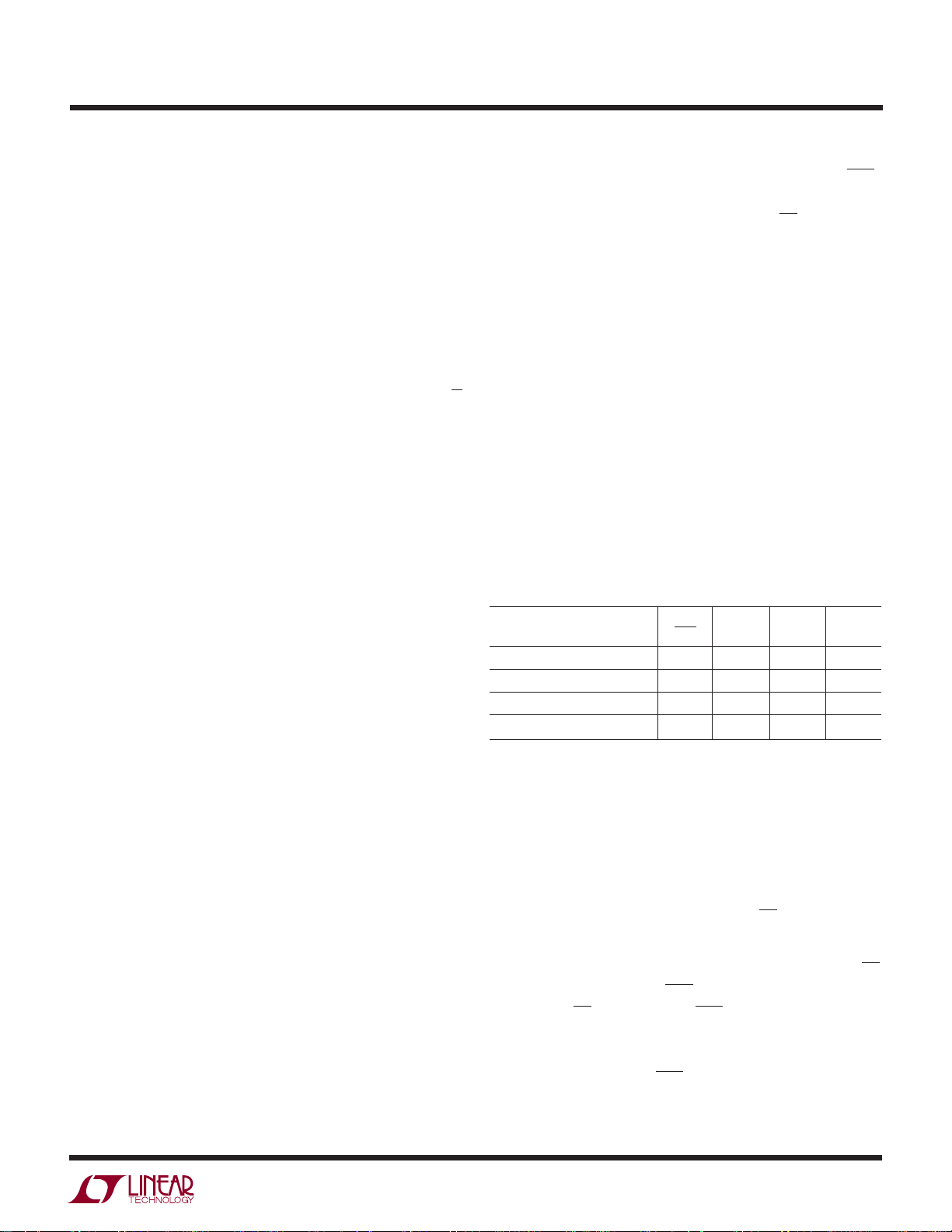
1.69k
SDO
24467 TA04
Hi-Z TO V
OL
VOH TO V
OL
VOL TO Hi-Z
C
LOAD
= 20pF
V
CC
UU
W
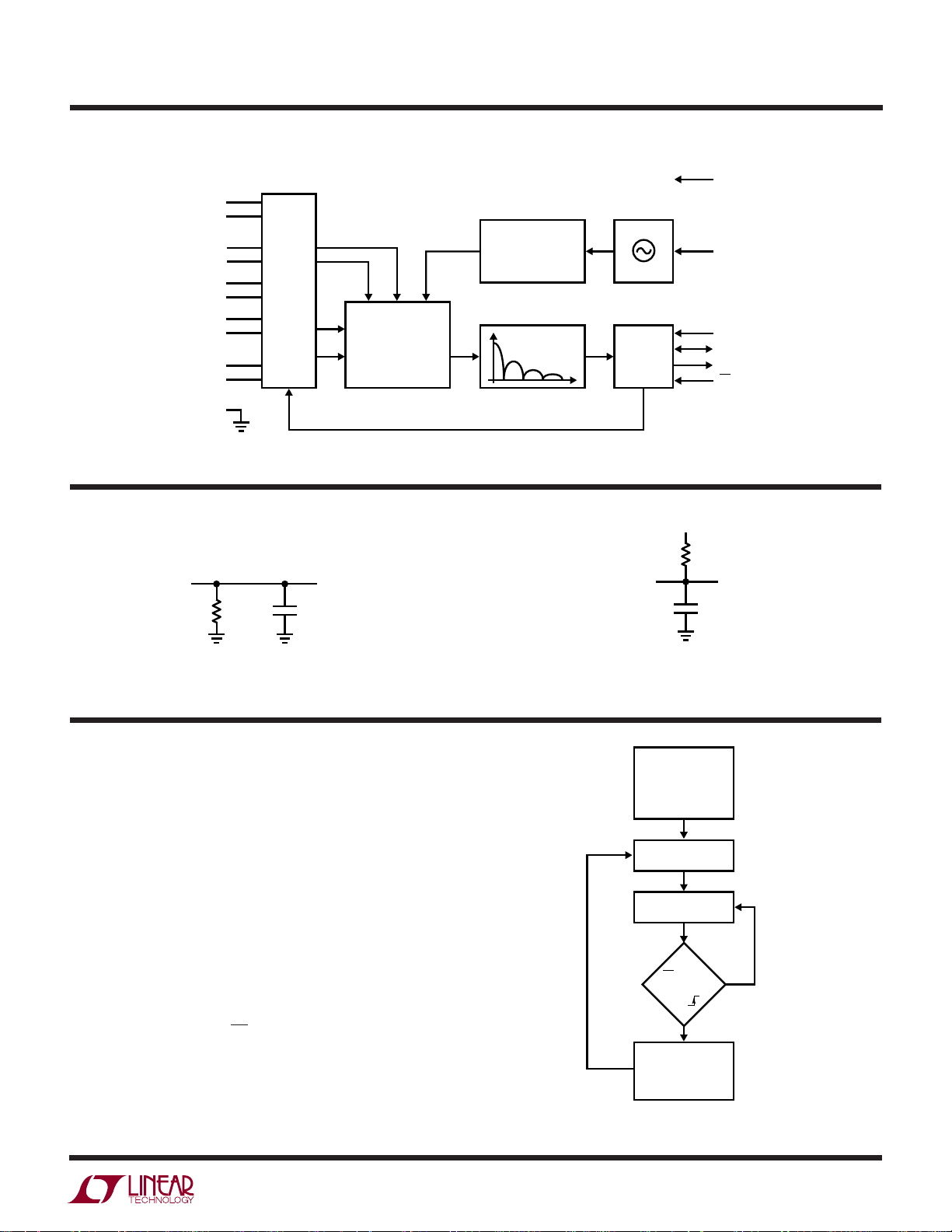
FU CTIO AL BLOCK DIAGRA
+
V
REF01
–
V
REF01
V
REF67
V
REF67
V
V
REFG
REFG
CH0
CH1
CH7
COM
GND
•
•
•
+
–
+
–
•
•
•
+
REF
–
REF
+
IN
INPUT/REFERENCE MUX
IN
–
∆Σ MODULATOR
DIFFERENTIAL
3RD ORDER
Figure 1. Functional Block Diagram
TEST CIRCUITS
AUTOCALIBRATION
AND CONTROL
DECIMATING FIR
ADDRESS
INTERNAL
OSCILLATOR
SERIAL
INTERFACE
24467 F01
V
CC
F
O
(INT/EXT)
SDI
SCK
SDO
CS
SDO
1.69k
Hi-Z TO V
VOL TO V
VOH TO Hi-Z
OH
OH
U
C
LOAD
= 20pF
24467 TA03
WUU
APPLICATIO S I FOR ATIO
CONVERTER OPERATION
Converter Operation Cycle
The LTC2446/LTC2447 are multichannel, multireference
high speed, delta-sigma analog-to-digital converters with
an easy to use 3- or 4-wire serial interface (see Figure 1).
Their operation is made up of three states. The converter
operating cycle begins with the conversion, followed by
the low power sleep state and ends with the data output/
input (see Figure 2). The 4-wire interface consists of serial
data input (SDI), serial data output (SDO), serial clock
(SCK) and chip select (CS). The interface, timing, operation cycle and data out format is compatible with Linear’s
entire family of ∆Σ converters.
Initially, the LTC2446/LTC2447 perform a conversion.
Once the conversion is complete, the device enters the
POWER UP
+
=CH0, IN–=CH1
IN
+
REF
REF
OSR=256,1X MODE
CONVERT
CS = LOW
AND
CHANNEL SELECT
REFERENCE SELECT
SPEED SELECT
DATA OUTPUT
= V
–
= V
SLEEP
SCK
REFO1
REF01
YES
+
,
–
24467 F02
NO
Figure 2. LTC2446/LTC2447 State Transition Diagram
24467fa
7

LTC2446/LTC2447
U
WUU
APPLICATIO S I FOR ATIO
sleep state. While in this sleep state, power consumption
is reduced below 10µA. The part remains in the sleep state
as long as CS is HIGH. The conversion result is held
indefinitely in a static shift register while the converter is
in the sleep state.
Once CS is pulled LOW, the device begins outputting the
conversion result. There is no latency in the conversion
result while operating in the 1x mode. The data output corresponds to the conversion just performed. This result is
shifted out on the serial data out pin (SDO) under the control of the serial clock (SCK). Data is updated on the falling
edge of SCK allowing the user to reliably latch data on the
rising edge of SCK (see Figure 3). The data output state is
concluded once 32 bits are read out of the ADC or when CS
is brought HIGH. The device automatically initiates a new
conversion and the cycle repeats.
Through timing control of the CS, SCK and EXT pins, the
LTC2446/LTC2447 offer several flexible modes of operation (internal or external SCK). These various modes do
not require programming configuration registers; moreover, they do not disturb the cyclic operation described
above. These modes of operation are described in detail in
the Serial Interface Timing Modes section.
Ease of Use
The LTC2446/LTC2447 data output has no latency, filter
settling delay or redundant data associated with the
conversion cycle while operating in the 1x mode. There
is a one-to-one correspondence between the conversion
and the output data. Therefore, multiplexing multiple
analog voltages and references is easy. Speed/resolution
adjustments may be made seamlessly between two
conversions without settling errors.
The LTC2446/LTC2447 perform offset and full-scale calibrations every conversion cycle. This calibration is transparent to the user and has no effect on the cyclic operation
described above. The advantage of continuous calibration
is extreme stability of offset and full-scale readings with respect to time, supply voltage change and temperature drift.
Power-Up Sequence
The LTC2446/LTC2447 automatically enter an internal
reset state when the power supply voltage V
drops
CC
below approximately 2.2V. This feature guarantees the
integrity of the conversion result and of the serial interface mode selection.
When the VCC voltage rises above this critical threshold,
the converter creates an internal power-on-reset (POR)
signal with a duration of approximately 0.5ms. The POR
signal clears all internal registers. The conversion immediately following a POR is performed on the input channel
+
IN
= CH0, IN– = CH1, REF+ = V
REF01
+
, REF– V
REF01
–
at an
OSR = 256 in the 1x mode. Following the POR signal, the
LTC2446/LTC2447 start a normal conversion cycle and
follow the succession of states described above. The first
conversion result following POR is accurate within the
specifications of the device if the power supply voltage is
restored within the operating range (4.5V to 5.5V) before
the end of the POR time interval.
Reference Voltage Range
These converters accept truly differential external reference voltages. Each set of five reference inputs may be
independently driven to any common mode voltage over
the entire supply range of the device (GND to V
CC
). For
correct converter operation, each positive reference pin
REF
+
(V
REF01
+
, V
REF23
+
, V
REF45
+
, V
REF67
+
, V
REFG
+
) must
be more positive than its corresponding negative reference pin REF
–
V
) by at least 100mV.
REFG
–
(V
REF01
–
, V
REF23
–
, V
REF45
–
, V
REF67
–
,
The LTC2446/LTC2447 can accept a differential reference
from 0.1V to V
on each set of reference input pins. The
CC
converter output noise is determined by the thermal noise
of the front-end circuits, and as such, its value in microvolts is nearly constant with reference voltage. A decrease
in reference voltage will not significantly improve the
converter’s effective resolution. On the other hand, a
reduced reference voltage will improve the converter’s
overall INL performance.
Input Voltage Range
The analog input is truly differential with an absolute/
common mode range for the CH0-CH7 and COM input
pins extending from GND – 0.3V to V
+ 0.3V. Outside
CC
these limits, the ESD protection devices begin to turn on
and the errors due to input leakage current increase
rapidly. Within these limits, the LTC2446/LTC2447
24467fa
8
LTC2446/LTC2447
U
WUU
APPLICATIO S I FOR ATIO
c
onvert the bipolar differential input signal, VIN = IN+ –
–
(where IN+ and IN– are the selected input channels),
IN
from –FS = –0.5 • V
+
REF
– REF– (REF+ and REF– are the selected references).
Outside this range, the converter indicates the overrange
or the underrange condition using distinct output codes.
MUXOUT/ADCIN
There are two differences between the LTC2446 and the
LTC2447. The first is the RMS noise performance. For a
given OSR, the LTC2447 noise level is approximately √2
times lower (0.5 effective bits)than that of the LTC2446.
The second difference is the LTC2447 includes MUXOUT/
ADCIN pins. These pins enable an external buffer or gain
block to be inserted between the selected input channel of
the multiplexer and the input to the ADC. Since the buffer
is driven by the output of the multiplexer, only one circuit
is required for all 8 input channels. Additionally, the
transparent calibration feature of the LTC244X family
automatically removes the offset errors of the external
buffer.
In order to achieve optimum performance, the MUXOUT
and ADCIN pins should not be shorted together. In applications where the MUXOUT and ADCIN need to be shorted
together, the LTC2446 should be used because the
MUXOUT and ADCIN are internally connected for optimum performance.
to +FS = 0.5 • V
REF
where V
REF
REF
=
Bit 31 (first output bit) is the end of conversion (EOC)
indicator. This bit is available at the SDO pin during the
conversion and sleep states whenever the CS pin is LOW.
This bit is HIGH during the conversion and goes LOW
when the conversion is complete.
Bit 30 (second output bit) is a dummy bit (DMY) and is
always LOW.
Bit 29 (third output bit) is the conversion result sign indicator (SIG). If V
is >0, this bit is HIGH. If VIN is <0, this
IN
bit is LOW.
Bit 28 (fourth output bit) is the most significant bit (MSB)
of the result. This bit in conjunction with Bit 29 also
provides the underrange or overrange indication. If both
Bit 29 and Bit 28 are HIGH, the differential input voltage is
above +FS. If both Bit 29 and Bit 28 are LOW, the
differential input voltage is below –FS.
The function of these bits is summarized in Table 1.
Table 1. LTC2446/LTC2447 Status Bits
BIT 31 BIT 30 BIT 29 BIT 28
INPUT RANGE EOC DMY SIG MSB
VIN ≥ 0.5 • V
0V ≤ VIN < 0.5 • V
–0.5 • V
VIN < – 0.5 • V
REF
≤ VIN < 0V 0001
REF
REF
REF
0011
0010
0000
Bits 28-5 are the 24-bit conversion result MSB first.
Output Data Format
The LTC2446/LTC2447 serial output data stream is 32 bits
long. The first 3 bits represent status information indicating the sign and conversion state. The next 24 bits are the
conversion result, MSB first. The remaining 5 bits are sub
LSBs beyond the 24-bit level that may be included in
averaging or discarded without loss of resolution. In the
case of ultrahigh resolution modes, more than 24 effective
bits of performance are possible (see Table 4). Under
these conditions, sub LSBs are included in the conversion
result and represent useful information beyond the 24-bit
level. The third and fourth bit together are also used to
indicate an underrange condition (the differential input
voltage is below –FS) or an overrange condition (the
differential input voltage is above +FS).
Bit 5 is the least significant bit (LSB).
Bits 4-0 are sub LSBs below the 24-bit level. Bits 4-0 may
be included in averaging or discarded without loss of
resolution.
Data is shifted out of the SDO pin under control of the serial
clock (SCK), see Figure 3. Whenever CS is HIGH, SDO
remains high impedance and SCK is ignored.
In order to shift the conversion result out of the device, CS
must first be driven LOW. EOC is seen at the SDO pin of the
device once CS is pulled LOW. EOC changes real time from
HIGH to LOW at the completion of a conversion. This
signal may be used as an interrupt for an external
microcontroller. Bit 31 (EOC) can be captured on the first
24467fa
9
 Loading...