

查询LTC2435-1CGN供应商
LTC2435/LTC2435-1
ADCs with Differential Input and
FEATURES
■
××
2
× Speed Up Version of the LTC2430: 15Hz Output
××
Rate, 60Hz Notch—LTC2435; 13.75Hz Output Rate,
Simultaneous 50Hz/60Hz Notch—LTC2435-1
■
Differential Input and Differential Reference with
GND to VCC Common Mode Range
■
3ppm INL, No Missing Codes
■
10ppm Gain Error
■
0.8ppm Noise
■
Single Conversion Settling Time for Multiplexed
Applications
■
Internal Oscillator—No External Components
Required
■
Single Supply 2.7V to 5.5V Operation
■
Low Supply Current (200µA,4µA in Auto Sleep)
■
20-Bit ADC in Narrow SSOP-16 Package
(SO-8 Footprint)
U
APPLICATIO S
■
Direct Sensor Digitizer
■
Weight Scales
■
Direct Temperature Measurement
■
Gas Analyzers
■
Strain Gage Transducers
■
Instrumentation
■
Data Acquisition
■
Industrial Process Control
■
6-Digit DVMs
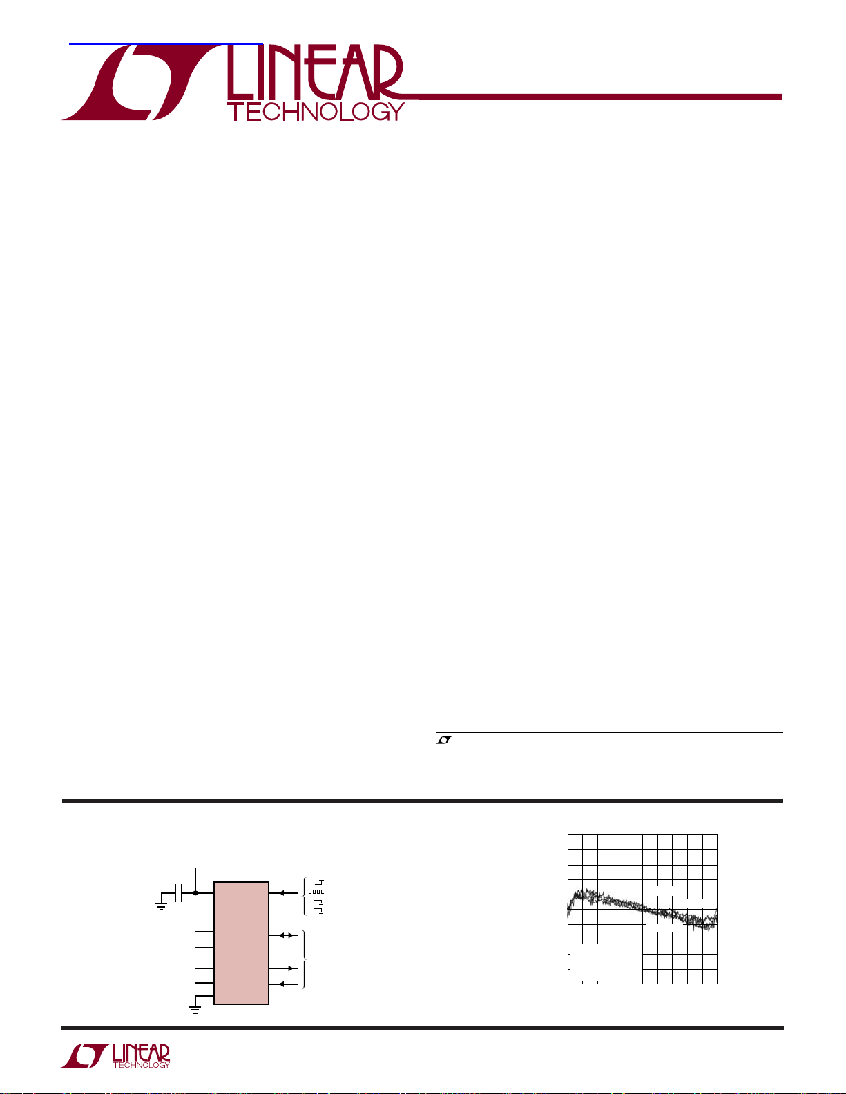
20-Bit No Latency ∆Σ
TM
Differential Reference
U
DESCRIPTIO
The LTC®2435/2435-1 are 2.7V to 5.5V micropower
20-bit differential ∆Σ analog to digital converters with
integrated oscillator, 3ppm INL and 0.8ppm RMS noise.
They use delta-sigma technology and provide single cycle
settling time for multiplexed applications. Through a
single pin, the LTC2435 can be configured for better than
110dB input differential mode rejection at 50Hz or 60Hz
±2%, or it can be driven by an external oscillator for a user
defined rejection frequency. The LTC2435-1 can be configured for better than 87dB input differential mode rejection over the range of 49Hz to 61.2Hz (50Hz and 60Hz
±2% simultaneously). The internal oscillator requires no
external frequency setting components.
The converters accept any external differential reference
voltage from 0.1V to VCC for flexible ratiometric and
remote sensing measurement configurations. The fullscale differential input range is from –0.5V
The reference common mode voltage, V
input common mode voltage, V
, may be indepen-
INCM
dently set anywhere within the GND to VCC range of the
LTC2435/LTC2435-1. The DC common mode input rejection is better than 120dB.
The LTC2435/LTC2435-1 communicate through a flexible
3-wire digital interface which is compatible with SPI and
MICROWIRETM protocols.
, LTC and LT are registered trademarks of Linear Technology Corporation.
No Latency ∆Σ is a trademark of Linear Technology Corporation.
MICROWIRE is a trademark of National Semiconductor Corporation.
Protected by U.S. Patents including 6140950, 6169506.
to 0.5V
REF
REFCM
REF
, and the
.
U
TYPICAL APPLICATIO S
2.7V TO 5.5V
1µF
214
V
F
CC
O
LTC2435/
LTC2435-1
3
+
REFERENCE
VOLTAGE
0.1V TO V
ANALOG INPUT RANGE
TO 0.5V
–0.5V
REF
1, 7, 8, 9, 10, 15, 16
REF
4
REF
CC
5
+
IN
REF
6
–
IN
GND
13
SCK
–
12
SDO
11
CS
V
CC
= INTERNAL OSC/50Hz REJECTION (LTC2435)
= EXTERNAL CLOCK SOURCE
= INTERNAL OSC/60Hz REJECTION (LTC2435)
= INTERNAL 50Hz/60Hz REJECTION (LTC2435-1)
3-WIRE
SPI INTERFACE
2435 TA01
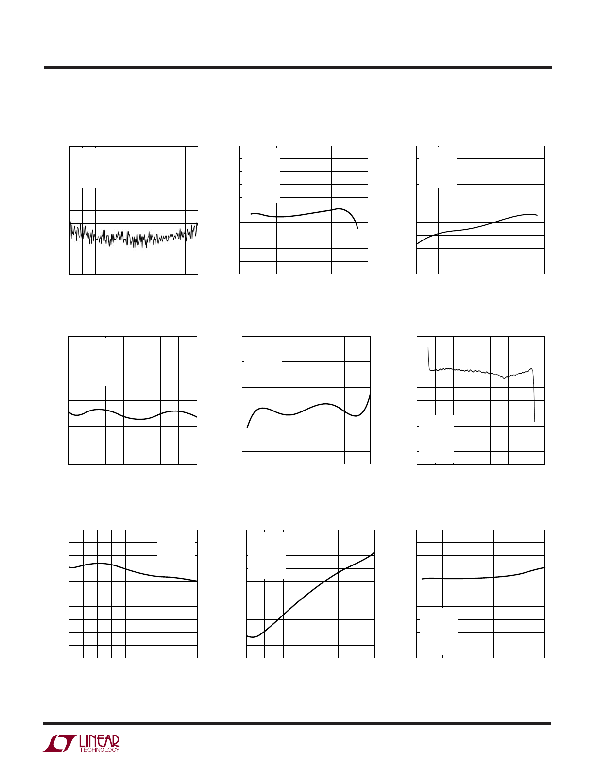
Integral Nonlinearity vs Input
10
8
6
4
)
REF
2
0
–2
INL (ppm OF V
–4
FO = GND
–6
= 5V
V
CC
= 5V
V
REF
–8
= V
V
INCM
–10
–2.5 –1.5 – 0.5 0.5 1.5
INCM
TA = 25°C
TA = 85°C
TA = –45°C
= 2.5V
INPUT VOLTAGE (V)
2435 G04
2.5
24351fa
1
LTC2435/LTC2435-1
WW
W
ABSOLUTE AXI U RATI GS
U
UUW
PACKAGE/ORDER I FOR ATIO
(Notes 1, 2)
Supply Voltage (VCC) to GND....................... –0.3V to 7V
Analog Input Pins Voltage
to GND .................................... –0.3V to (V
+ 0.3V)
CC
Reference Input Pins Voltage
to GND .................................... –0.3V to (VCC + 0.3V)
Digital Input Voltage to GND ........ –0.3V to (VCC + 0.3V)
Digital Output Voltage to GND ..... – 0.3V to (VCC + 0.3V)
Operating Temperature Range
LTC2435C/LTC2435-1C........................... 0°C to 70°C
LTC2435I/LTC2435-1I ........................ –40°C to 85°C
Storage Temperature Range ................. –65°C to 150°C
Lead Temperature (Soldering, 10 sec).................. 300°C
ELECTRICAL CHARACTERISTICS
The ● denotes specifications which apply over the full operating
TOP VIEW
1
GND
2
V
CC
+
3
REF
–
4
REF
+
5
IN
–
6
IN
7
GND
8
GND
GN PACKAGE
16-LEAD PLASTIC SSOP
T
= 125°C, θJA = 95°C/W
JMAX
Consult LTC Marketing for parts specified with wider operating temperature ranges.
16
GND
15
GND
14
F
O
13
SCK
12
SDO
11
CS
10
GND
9
GND
ORDER PART NUMBER
LTC2435CGN
LTC2435IGN
LTC2435-1CGN
LTC2435-1IGN
GN PART MARKING
2435
2435I
24351
24351I
temperature range, otherwise specifications are at TA = 25°C. (Notes 3, 4)
PARAMETER CONDITIONS MIN TYP MAX UNITS
Resolution (No Missing Codes) 0.1V ≤ V
Integral Nonlinearity 5V ≤ VCC ≤ 5.5V, REF+ = 2.5V, REF– = GND, V
5V ≤ VCC ≤ 5.5V, REF+ = 5V, REF– = GND, V
2.7V ≤ VCC ≤ 5.5V, REF+ = 2.5V, REF– = GND, V
Offset Error 2.5V ≤ REF+ ≤ VCC, REF– = GND, ● 25 mV
GND ≤ IN
Offset Error Drift 2.5V ≤ REF+ ≤ VCC, REF– = GND, 100 nV/°C
GND ≤ IN
Positive Gain Error 2.5V ≤ REF+ ≤ VCC, REF– = GND, ● 10 25 ppm of V
IN+ = 0.75REF+, IN– = 0.25 • REF
Positive Gain Error Drift 2.5V ≤ REF+ ≤ VCC, REF– = GND, 0.1 ppm of V
Negative Gain Error 2.5V ≤ REF+ ≤ VCC, REF– = GND, ● 10 25 ppm of V
Negative Gain Error Drift 2.5V ≤ REF+ ≤ VCC, REF– = GND, 0.1 ppm of V
Output Noise 5V ≤ VCC ≤ 5.5V, REF+ = 5V, REF– = GND, 4 µV
+
IN
IN+ = 0.25 • REF+, IN– = 0.75 • REF
+
IN
GND ≤ IN– = IN+ ≤ VCC, (Note 13)
≤ VCC, –0.5 • V
REF
+
= IN– ≤ VCC, (Note 14)
+
= IN– ≤ V
= 0.75REF+, IN– = 0.25 • REF
= 0.25 • REF+, IN– = 0.75 • REF
CC
≤ VIN ≤ 0.5 • V
REF
+
+
, (Note 5) ● 20 Bits
REF
= 1.25V, (Note 6) 2 ppm of V
INCM
= 2.5V, (Note 6) ● 3 20 ppm of V
INCM
= 1.25V, (Note 6) 10 ppm of V
INCM
+
+
REF
REF
REF
REF
REF
REF
/°C
REF
/°C
RMS
U
CO VERTER CHARACTERISTICS
temperature range, otherwise specifications are at TA = 25°C. (Notes 3, 4)
PARAMETER CONDITIONS MIN TYP MAX UNITS
Input Common Mode Rejection DC 2.5V ≤ REF+ ≤ VCC, REF– = GND, ● 110 120 dB
GND ≤ IN
–
= IN+ ≤ VCC (Note 5)
The ● denotes specifications which apply over the full operating
24351fa
2
LTC2435/LTC2435-1
U
CO VERTER CHARACTERISTICS
temperature range, otherwise specifications are at TA = 25°C. (Notes 3, 4)
PARAMETER CONDITIONS MIN TYP MAX UNITS
Input Common Mode Rejection 2.5V ≤ REF+ ≤ VCC, REF– = GND, ● 140 dB
60Hz ±2% (LTC2435) GND ≤ IN
Input Common Mode Rejection 2.5V ≤ REF+ ≤ VCC, REF– = GND, ● 140 dB
50Hz ±2% (LTC2435) GND ≤ IN
Input Normal Mode Rejection (Notes 5, 7) ● 110 120 dB
60Hz ±2% (LTC2435)
Input Normal Mode Rejection (Notes 5, 8) ● 110 120 dB
50Hz ±2% (LTC2435)
Input Common Mode Rejection 2.5V ≤ REF+ ≤ VCC, REF– = GND, ● 120 dB
49Hz to 61.2Hz (LTC2435-1) GND ≤ IN
Input Normal Mode Rejection FO = GND (Note 5) ● 87 dB
49Hz to 61.2Hz (LTC2435-1)
Input Normal Mode Rejection External Oscillator (Note 5) ● 87 dB
External Clock f
Input Normal Mode Rejection External Oscillator (Note 5) ● 110 120 dB
External Clock f
Reference Common Mode 2.5V ≤ REF+ ≤ VCC, GND ≤ REF– ≤ 2.5V, ● 130 140 dB
Rejection DC V
Power Supply Rejection, DC REF+ = VCC, REF– = GND, IN– = IN+ = GND 100 dB
Power Supply Rejection, 60Hz ±2% REF+ = 2.5V, REF– = GND, IN– = IN+ = GND, (Note 7) 120 dB
Power Supply Rejection, 50Hz ±2% REF+ = 2.5V, REF– = GND, IN– = IN+ = GND, (Note 8) 120 dB
/2560 ±14%
EOSC
/2560 ±4%
EOSC
–
= IN+ ≤ VCC, (Notes 5, 7)
–
= IN+ ≤ VCC, (Notes 5, 8)
–
= IN+ ≤ VCC, (Notes 5, 7)
= 2.5V, IN– = IN+ = GND (Note 5)
REF
The ● denotes specifications which apply over the full operating
UUU
A ALOG I PUT AUD REFERE CE
temperature range, otherwise specifications are at TA = 25°C. (Note 3)
SYMBOL PARAMETER CONDITIONS MIN TYP MAX UNITS
+
IN
–
IN
V
IN
+
REF
–
REF
V
REF
CS (IN+)IN
CS (IN–)IN
CS (REF+)REF
CS (REF–)REF
I
I
I
I
(IN+)IN+ DC Leakage Current CS = VCC, IN+ = GND ● –10 1 10 nA
DC_LEAK
(IN–)IN– DC Leakage Current CS = VCC, IN– = V
DC_LEAK
(REF+)REF+ DC Leakage Current CS = VCC, REF+ = V
DC_LEAK
(REF–)REF– DC Leakage Current CS = VCC, REF– = GND ● –10 1 10 nA
DC_LEAK
Absolute/Common Mode IN+ Voltage ● GND – 0.3V VCC + 0.3V V
Absolute/Common Mode IN– Voltage ● GND – 0.3V VCC + 0.3V V
Input Differential Voltage Range ● –V
+
(IN
– IN–)
Absolute/Common Mode REF+ Voltage ● 0.1 V
Absolute/Common Mode REF– Voltage ● GND VCC – 0.1V V
Reference Differential Voltage Range ● 0.1 V
+
(REF
– REF–)
+
Sampling Capacitance 1.5 pF
–
Sampling Capacitance 1.5 pF
+
Sampling Capacitance 1.5 pF
–
Sampling Capacitance 1.5 pF
The ● denotes specifications which apply over the full operating
CC
CC
/2 V
REF
● –10 1 10 nA
● –10 1 10 nA
/2 V
REF
CC
CC
V
V
24351fa
3
LTC2435/LTC2435-1
UU
DIGITAL I PUTS A D DIGITAL OUTPUTS
operating temperature range, otherwise specifications are at T
SYMBOL PARAMETER CONDITIONS MIN TYP MAX UNITS
V
IH
V
IL
V
IH
V
IL
I
IN
I
IN
C
IN
C
IN
V
OH
V
OL
V
OH
V
OL
I
OZ
High Level Input Voltage 2.7V ≤ VCC ≤ 5.5V ● 2.5 V
CS, F
O
Low Level Input Voltage 4.5V ≤ VCC ≤ 5.5V ● 0.8 V
CS, F
O
High Level Input Voltage 2.7V ≤ VCC ≤ 5.5V (Note 9) ● 2.5 V
SCK 2.7V ≤ V
Low Level Input Voltage 4.5V ≤ VCC ≤ 5.5V (Note 9) ● 0.8 V
SCK 2.7V ≤ V
Digital Input Current 0V ≤ VIN ≤ V
CS, F
O
Digital Input Current 0V ≤ VIN ≤ VCC (Note 9) ● –10 10 µA
SCK
Digital Input Capacitance 10 pF
CS, F
O
Digital Input Capacitance (Note 9) 10 pF
SCK
High Level Output Voltage IO = –800µA ● VCC – 0.5 V
SDO
Low Level Output Voltage IO = 1.6mA ● 0.4 V
SDO
High Level Output Voltage IO = –800µA (Note 10) ● VCC – 0.5 V
SCK
Low Level Output Voltage IO = 1.6mA (Note 10) ● 0.4 V
SCK
Hi-Z Output Leakage ● –10 10 µA
SDO
2.7V ≤ VCC ≤ 3.3V 2.0 V
2.7V ≤ VCC ≤ 5.5V 0.6 V
= 25°C. (Note 3)
A
≤ 3.3V (Note 9) 2.0 V
CC
≤ 5.5V (Note 9) 0.6 V
CC
CC
The ● denotes specifications which apply over the full
● –10 10 µA
WU
POWER REQUIRE E TS
otherwise specifications are at TA = 25°C. (Note 3)
SYMBOL PARAMETER CONDITIONS MIN TYP MAX UNITS
V
CC
I
CC
Supply Voltage ● 2.7 5.5 V
Supply Current
Conversion Mode CS = 0V (Note 12)
Sleep Mode CS = V
Sleep Mode CS = V
The ● denotes specifications which apply over the full operating temperature range,
● 200 300 µA
(Note 12) ● 410 µA
CC
, 2.7V ≤ VCC ≤ 3.3V (Note 12) ● 2 µA
CC
24351fa
4
LTC2435/LTC2435-1
WU
TI I G CHARACTERISTICS
range, otherwise specifications are at T
SYMBOL PARAMETER CONDITIONS MIN TYP MAX UNITS
f
EOSC
t
HEO
t
LEO
t
CONV
f
ISCK
D
ISCK
f
ESCK
t
LESCK
t
HESCK
t
DOUT_ISCK
t
DOUT_ESCK
t
1
t2 CS ↑ to SDO High Z ● 0 200 ns
t3 CS ↓ to SCK ↓ (Note 10) ● 0 200 ns
t4 CS ↓ to SCK ↑ (Note 9) ● 50 ns
t
KQMAX
t
KQMIN
t
5
t
6
Note 1: Absolute Maximum Ratings are those values beyond which the
life of the device may be impaired.
Note 2: All voltage values are with respect to GND.
Note 3: VCC = 2.7 to 5.5V unless otherwise specified.
V
= REF+ – REF–, V
REF
= IN+ – IN–, V
V
IN
Note 4: FO pin tied to GND or to VCC or to external conversion clock
source with f
Note 5: Guaranteed by design, not subject to test.
Note 6: Integral nonlinearity is defined as the deviation of a code from
a straight line passing through the actual endpoints of the transfer
curve. The deviation is measured from the center of the quantization
band.
Note 7: FO = 0V (internal oscillator) or f
(external oscillator) for the LTC2435 or f
LTC2435-1.
External Oscillator Frequency Range ● 5 2000 kHz
External Oscillator High Period ● 0.25 200 µs
External Oscillator Low Period ● 0.25 200 µs
Conversion Time (LTC2435) FO = 0V ● 65.6 66.9 68.3 ms
Conversion Time (LTC2435-1) FO = 0V ● 72 73.5 75 ms
Internal SCK Frequency Internal Oscillator (Note 10), LTC2435 19.2 kHz
Internal SCK Duty Cycle (Note 10) ● 45 55 %
External SCK Frequency Range (Note 9) ● 2000 kHz
External SCK Low Period (Note 9) ● 250 ns
External SCK High Period (Note 9) ● 250 ns
Internal SCK 24-Bit Data Output Time Internal Oscillator (Notes 10, 12), LTC2435 ● 1.22 1.25 1.28 ms
External SCK 24-Bit Data Output Time (Note 9) ● 24/f
CS ↓ to SDO Low Z ● 0 200 ns
SCK ↓ to SDO Valid ● 220 ns
SDO Hold After SCK ↓ (Note 5) ● 15 ns
SCK Set-Up Before CS ↓ ● 50 ns
SCK Hold After CS ↓ ● 50 ns
= (REF+ + REF–)/2;
REFCM
= (IN+ + IN–)/2.
INCM
= 153600Hz unless otherwise specified.
EOSC
= 25°C. (Note 3)
A
= 153600Hz ±2%
EOSC
= 139800Hz ±2% for the
EOSC
The ● denotes specifications which apply over the full operating temperature
F
= V
O
CC
External Oscillator (Note 11)
External Oscillator (Note 11)
Internal Oscillator (Note 10), LTC2435-1 17.5 kHz
External Oscillator (Notes 10, 11) f
Internal Oscillator (Notes 10, 12), LTC2435-1
External Oscillator (Notes 10, 11)
Note 8: FO = VCC (internal oscillator) or f
(external oscillator).
Note 9: The converter is in external SCK mode of operation such that
the SCK pin is used as digital input. The frequency of the clock signal
driving SCK during the data output is f
Note 10: The converter is in internal SCK mode of operation such that
the SCK pin is used as digital output. In this mode of operation the
SCK pin has a total equivalent load capacitance C
Note 11: The external oscillator is connected to the FO pin. The external
oscillator frequency, f
Note 12: The converter uses the internal oscillator.
= 0V or FO = VCC.
F
O
Note 13: The output noise includes the contribution of the internal
calibration operations.
Note 14: Refer to Offset Accuracy and Drift in the Applications
Information section.
● 78.7 80.3 81.9 ms
● 10278/f
● 10278/f
● 1.34 1.37 1.40 ms
● 192/f
ESCK
, is expressed in kHz.
EOSC
(in kHz) ms
EOSC
(in kHz) ms
EOSC
/8 kHz
EOSC
(in kHz) ms
EOSC
(in kHz) ms
ESCK
= 128000Hz ±2%
EOSC
and is expressed in kHz.
= 20pF.
LOAD
24351fa
5

LTC2435/LTC2435-1
–320
–330
–340
–350
–360
TUE (ppm OF V
REF
)
FO = GND
V
CC
= 2.7V
V
REF
= 2.5V
V
INCM
= V
INCM
= 1.25V
INPUT VOLTAGE (V)
–1.25 – 0.75 –0.25 0.25 0.75
2435 G03
1.25
TA = –45°C
TA = 25°C
TA = 85°C
UW
TYPICAL PERFOR A CE CHARACTERISTICS
Total Unadjusted Error (V
V
= 5V)
REF
–340
FO = GND
V
= 5V
CC
= 5V
V
REF
= V
V
INCM
–345
)
REF
–350
TUE (ppm OF V
–355
–360
–2.5
= 2.5V
INCM
TA = 85°C
–1.5
–0.5
INPUT VOLTAGE (V)
Integral Nonlinearity (V
V
= 5V)
REF
10
8
6
4
)
REF
2
0
–2
INL (ppm OF V
–4
FO = GND
–6
= 5V
V
CC
= 5V
V
REF
–8
–10
= V
V
INCM
–2.5 –1.5 –0.5 0.5 1.5
= 2.5V
INCM
INPUT VOLTAGE (V)
30
25
20
15
10
NUMBER OF READINGS (%)
5
0
–330
= 5V,
CC
–680
–685
)
–690
REF
–695
–700
TUE (ppm OF V
–705
–710
–1.25
Integral Nonlinearity (V
TA = 25°C
0.5
TA = –45°C
1.5
= 5V,
CC
2.5
2435 G01
V
3
2
)
TA = 25°C
TA = 85°C
TA = –45°C
2.5
2435 G04
1
REF
0
–1
INL (ppm OF V
–2
–3
–1.25 –0.75 –0.25 0.25 0.75
Noise Histogram (Output Rate =
15Hz, VCC = 5V, V
10,000 CONSECUTIVE READINGS
= 5V
V
CC
= 5V
V
REF
= 0V
V
IN
= 2.5V
V
INCM
= GND
F
O
= 25°C
T
A
–329 –327
–328
OUTPUT CODE(ppm OF V
= 5V)
REF
GAUSSIAN
DISTRIBUTION
m = –325.4ppm
σ = 0.79ppm
–324
–323
REF
–325 –321
–326
–322
)
2435 G07
Total Unadjusted Error (V
V
= 2.5V)
REF
FO = GND
= 5V
V
CC
= 2.5V
V
REF
= V
V
INCM
REF
FO = GND
= 5V
V
CC
V
REF
V
INCM
= 1.25V
INCM
TA = 25°C
TA = 85°C
–0.75 –0.25 0.25 0.75
INPUT VOLTAGE (V)
CC
= 2.5V)
TA = –45°C
TA = 85°C
TA = 25°C
= 2.5V
= V
= 1.25V
INCM
INPUT VOLTAGE (V)
NUMBER OF READINGS (%)
= 5V,
CC
TA = –45°C
2435 G02
= 5V,
2435 G05
1.25
1.25
Total Unadjusted Error (V
V
= 2.5V)
REF
Integral Nonlinearity (V
V
= 2.5V)
REF
10
FO = GND
= 2.7V
V
8
CC
= 2.5V
V
REF
6
= V
V
INCM
4
)
REF
2
0
–2
INL (ppm of V
–4
–6
–8
–10
–1.25 – 0.75 –0.25 0.25 0.75
INCM
Noise Histogram (Output Rate =
15Hz, VCC = 2.7V, V
14
10,000 CONSECUTIVE READINGS
= 2.7V
V
CC
12
= 2.5V
V
REF
= 0V
V
IN
= 2.5V
V
10
INCM
= GND
F
O
= 25°C
T
A
8
6
4
2
0
–372 –370 –368 –366 –364 –362 –360 –358
OUTPUT CODE (ppm OF V
= 2.5V)
REF
GAUSSIAN
DISTRIBUTION
m = –365ppm
σ = 1.55ppm
= 1.25V
TA = –45°C
INPUT VOLTAGE (V)
)
REF
2435 G08
CC
= 2.7V,
CC
TA = 25°C
= 2.7V,
TA = 85°C
1.25
2435 G06
24351fa
6
UW
TEMPERATURE (°C)
–50
RMS NOISE (µV)
5.0
4.8
4.6
4.4
4.2
4.0
3.8
3.6
3.4
3.2
3.0
0
50
75
2435 G12
–25
25
100
FO = GND
V
CC
= 5V
V
REF
= 5V
V
IN
= 0V
V
INCM
= GND
TYPICAL PERFOR A CE CHARACTERISTICS
LTC2435/LTC2435-1
RMS Noise vs Input Differential
Voltage
1.5
VCC = 5V
= 5V
V
1.4
REF
V
= 2.5V
INCM
1.3
)
RMS NOISE (ppm OF V
= GND
F
O
REF
= 25°C
T
A
1.2
1.1
1.0
0.9
0.8
0.7
0.6
0.5
–2.5 –2 –1.5 –1
INPUT DIFFERENTIAL VOLTAGE (V)
RMS Noise vs V
5.0
FO = GND
+
4.8
= V
REF
REF– = GND
4.6
= 25°C
T
A
= 0V
V
IN
4.4
4.2
4.0
3.8
RMS NOISE (µV)
3.6
3.4
3.2
3.0
2.7
V
INCM
= GND
3.1
–0.5
0.5 1 1.5 2 2.5
0
= V
CC
CC
4.3
3.9
3.5
VCC (V)
REF
4.7
5.1
2435 G10
2435 G13
5.5
RMS Noise vs V
5.0
FO = GND
+
4.8
= 5V
REF
–
= GND
REF
4.6
= 25°C
T
A
= 5V
V
CC
4.4
V
= 0V
IN
4.2
V
INCM
4.0
3.8
RMS NOISE (µV)
3.6
3.4
3.2
3.0
–1
0
RMS Noise vs V
5.0
FO = GND
–
4.8
REF
= 25°C
T
A
4.6
= 5V
V
CC
= 0V
V
IN
4.4
V
INCM
4.2
4.0
3.8
RMS NOISE (µV)
3.6
3.4
3.2
3.0
0
= GND
= GND
= GND
1
INCM
1
V
INCM
4
(V)
3
2
5
6
2435 G11
REF
4
3
2
V
(V)
REF
5
2435 G14
RMS Noise vs Temperature (TA)
Offset Error vs V
–320
–322
)
–324
REF
–326
–328
–330
–332
VCC = 5V
–1
REF
REF
V
F
T
IN
O
A
+
= 5V
–
= GND
= 0V
= GND
= 25°C
0
–334
–336
OFFSET ERROR (ppm OF V
–338
–340
INCM
3
2
1
V
(V)
INCM
5
6
2435 G15
4
Offset Error vs Temperature Offset Error vs V
–320
–322
)
–324
REF
–326
–328
–330
–332
–334
–336
OFFSET ERROR (ppm OF V
–338
–340
–45 –15
–30 0
TEMPERATURE (°C)
15
VCC = 5V
= 5V
V
REF
= 0V
V
IN
= GND
V
INCM
= GND
F
O
60
30 90
45
75
2435 G16
–320
REF+ = V
–322
)
–324
REF
–326
–328
–330
–332
–334
–336
OFFSET ERROR (ppm OF V
–338
–340
2.7
CC
REF– = GND
= 0V
V
IN
= GND
V
INCM
= GND
F
O
= 25°C
T
A
3.1
3.5
= V
CC
REF
4.7
3.9 5.5
4.3
V
(V)
CC
5.1
2435 G17
Offset Error vs V
–1.60
–1.61
–1.62
–1.63
–1.64
–1.65
–1.66
FO = GND
0
REF
T
V
V
V
A
CC
IN
INCM
–
= GND
= 25°C
= 5V
= 0V
= GND
1
–1.67
OFFSET ERROR (mV)
–1.68
–1.69
–1.70
REF
2
V
(V)
REF
5
2435 G18
24351fa
4
3
7
LTC2435/LTC2435-1
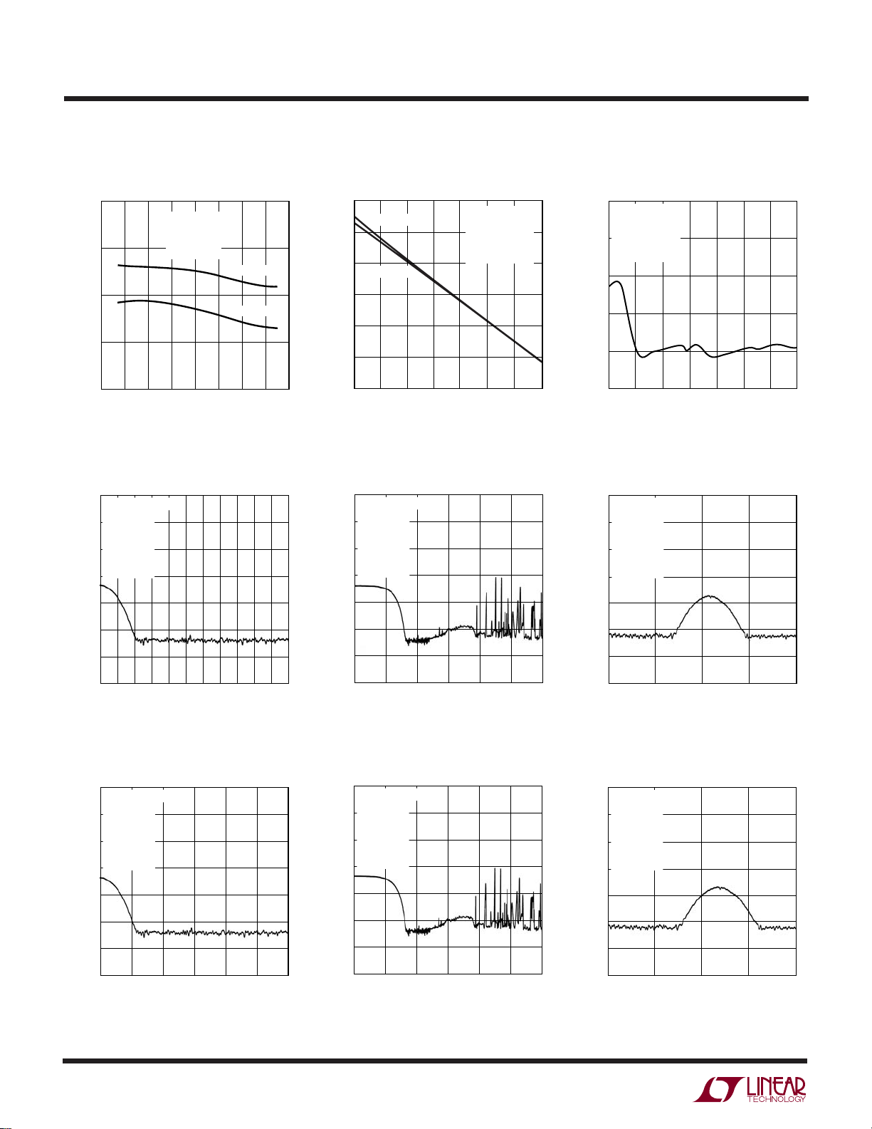
REJECTION (dB)
0
–20
–40
–60
–80
–100
–120
–140
FREQUENCY AT V
CC
(Hz)
13800 13950
2435 G24
13850 13900 14000
VCC = 4.1V
DC
±0.7V
REF+ = 2.5V
REF
–
= GND
IN
+
= GND
IN
–
= GND
F
O
= GND
T
A
= 25°C
UW
TYPICAL PERFOR A CE CHARACTERISTICS
Full-Scale Error vs Temperature Full-Scale Error vs V
–330
)
REF
–340
–350
–360
FULL-SCALE ERROR (ppm OF V
–370
–60 100
PSRR vs Frequency at V
FO = GND
= 5V
V
CC
= 5V
V
REF
= 2.5V
V
INCM
–20
20
TEMPERATURE (°C)
+FS ERROR
–FS ERROR
60–40 0 40
CC
(LTC2435-1)
0
–20
–40
–60
VCC = 4.1V
REF
REF
+
IN
–
IN
= GND
F
O
= 25°C
T
A
+
= 2.5V
–
= GND
= GND
= GND
DC
±1.4V
80
2435 G19
–300
)
–400
REF
–500
–600
–700
–800
FULL-SCALE ERROR(ppm OF V
–900
+FS ERROR
–FS ERROR
2.7
3.1 3.5
PSRR vs Frequency at V
(LTC2435-1)
0
VCC = 4.1V
DC
REF+ = 2.5V
–
–20
–40
–60
REF
IN
IN
F
O
T
+
–
A
= GND
= GND
= GND
= GND
= 25°C
CC
V
REF
–
REF
V
INCM
FO = GND
= 25°C
T
A
4.3 5.1 5.5
3.9 4.7
VCC (V)
= 2.5V
= GND
= 0.5V
CC
REF
2435 G20
+Full-Scale Gain Error vs V
20
V
= 2.5V
REF
–
= GND
REF
)
REF
+FS GAIN ERROR (ppm OF V
15
10
5
0
–5
V
INCM
FO = GND
T
A
2.7
= 0.5V
= 25°C
3.1
REF
3.9 5.5
3.5
V
CC
PSRR vs Frequency at V
(LTC2435-1)
(V)
4.3
4.7
CC
5.1
2435 G21
CC
REJECTION (dB)
REJECTION (dB)
–80
–100
–120
–140
0
60 80
40
20
FREQUENCY AT VCC (Hz)
PSRR vs Frequency at V
(LTC2435)
0
–20
–40
–60
–80
–100
–120
–140
VCC = 4.1V
REF
REF
+
IN
–
IN
= GND
F
O
= 25°C
T
A
0
±1.4V
DC
+
= 2.5V
–
= GND
= GND
= GND
80 120 160 200 240
40
FREQUENCY AT V
–80
REJECTION (dB)
–100
–120
–140
200 220180160140120100
2435 G22
CC
1
PSRR vs Frequency at V
(LTC2435)
0
VCC = 4.1V
REF+ = 2.5V
–20
REF
IN
IN
–40
F
O
T
A
–60
–80
REJECTION (dB)
–100
–120
–140
1
(Hz)
CC
2435 G25
100 1000 10000 1000001000000
10
FREQUENCY AT VCC (Hz)
DC
–
= GND
+
= GND
–
= GND
= GND
= 25°C
100 1000 10000 1000001000000
10
FREQUENCY AT VCC (Hz)
CC
2435 G23
2435 G26
PSRR vs Frequency at V
(LTC2435)
0
VCC = 4.1V
REF+ = 2.5V
–20
REF
+
IN
–
IN
–40
= GND
F
O
= 25°C
T
A
–60
–80
REJECTION (dB)
–100
–120
–140
15250 15400
±0.7V
DC
–
= GND
= GND
= GND
15300 15350 15450
FREQUENCY AT V
CC
(Hz)
CC
2435 G27
24351fa
8
UW
TYPICAL PERFOR A CE CHARACTERISTICS
LTC2435/LTC2435-1
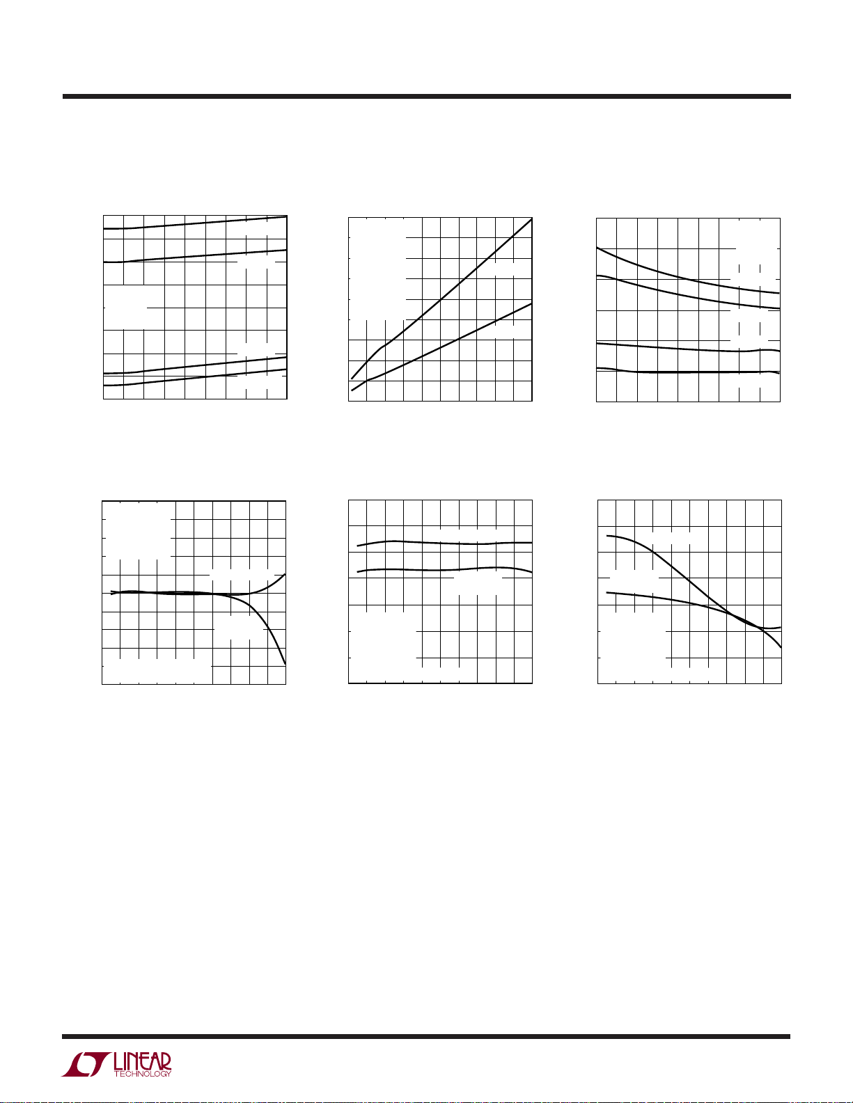
Conversion Current vs
Temperature
240
230
220
210
FO = GND
CS = GND
200
SCK = NC
SDO = NC
190
180
CONVERSION CURRENT (µA)
170
160
–45
–30 –15
TEMPERATURE (°C)
Offset Change* vs Output Data
Rate
50
V
= V
INCM
REFCM
VIN = 0V
40
)
REF
OFFSET CHANGE* (ppm OF V
–
= GND
REF
30
= EXT OSC
F
O
= 25°C
T
A
20
10
0
–10
–20
–30
* RELATIVE TO OFFSET AT
–40
NORMAL OUTPUT RATE
–50
0 204060
OUTPUT DATA RATE (READINGS/SEC)
80
VCC = V
120 140 160 180 200
100
VCC = 5.5V
VCC = 5V
VCC = 3V
VCC = 2.7V
45 60 75 9030150
REF
VCC = 2.7V
= 2.5V
V
REF
= 5V
2435 G28
2435 G31
Conversion Current vs
Output Data Rate
1000
V
= V
REF
CC
IN+ = GND
900
–
= GND
IN
SCK = NC
800
SDO = NC
700
SDI = GND
CS = GND
600
= EXT OSC
F
O
= 25°C
T
A
500
400
SUPPLY CURRENT (µA)
300
200
100
0102030
OUTPUT DATA RATE (READINGS/SEC)
Resolution (Noise
Output Data Rate
22
21
20
19
18
V
= V
INCM
RESOLUTION (BITS)
17
16
15
0 204060
REFCM
VIN = 0V
–
= GND
REF
= EXT OSC
F
O
= 25°C
T
A
RES = LOG
2
OUTPUT DATA RATE (READINGS/SEC)
Sleep-Mode Current vs
Temperature
40
60 70 80 90 100
50
RMS
VCC = 5V
VCC = 3V
2435 G29
≤ 1LSB) vs
6
5
4
3
2
SLEEP-MODE CURRENT (µA)
1
0
–45
–30 –15
Resolution (INL
TEMPERATURE (°C)
MAX
FO = GND
CS = V
SCK = NC
SDO = NC
VCC = 5.5V
VCC = 5V
VCC = 3V
VCC = 2.7V
45 60 75 9030150
≤ 1LSB) vs
CC
2435 G30
Output Data Rate
21
VCC = V
(V
/NOISE
REF
80
100
= 5V
REF
VCC = 2.7V
= 2.5V
V
REF
)
RMS
120 140 160 180 200
2435 G32
20
19
18
17
V
RESOLUTION (BITS)
VIN = 0V
16
REF
F
15
T
RES = LOG
14
0 204060
VCC = V
VCC = 2.7V
= 2.5V
V
REF
= V
INCM
REFCM
–
= GND
= EXT OSC
O
= 25°C
A
(V
/INL
2
REF
80
OUTPUT DATA RATE (READINGS/SEC)
= 5V
REF
)
MAX
120 140 160 180 200
100
2435 G33
24351fa
9

LTC2435/LTC2435-1
UUU
PI FU CTIO S
GND (Pins 1, 7, 8, 9, 10, 15, 16): Ground. Multiple ground
pins internally connected for optimum ground current flow
and V
ground plane through a low impedance connection. All seven
pins must be connected to ground for proper operation.
VCC (Pin 2): Positive Supply Voltage. Bypass to GND
(Pin 1) with a 10µF tantalum capacitor in parallel with
0.1µF ceramic capacitor as close to the part as possible.
REF+ (Pin 3), REF– (Pin 4): Differential Reference Input.
The voltage on these pins can have any value between GND
and V
maintained more positive than the reference negative
input, REF–, by at least 0.1V.
IN+ (Pin 5), IN– (Pin 6): Differential Analog Input. The
voltage on these pins can have any value between
GND – 0.3V and VCC + 0.3V. Within these limits the
converter bipolar input range (VIN = IN+ – IN–) extends
from – 0.5 • (V
the converter produces unique overrange and underrange
output codes.
CS (Pin 11): Active LOW Digital Input. A LOW on this pin
enables the SDO digital output and wakes up the ADC.
Following each conversion, the ADC automatically enters
the Sleep mode and remains in this low power state as
long as CS is HIGH. A LOW-to-HIGH transition on CS
during the Data Output transfer aborts the data transfer
and starts a new conversion.
decoupling. Connect each one of these pins to a
CC
as long as the reference positive input, REF+, is
CC
) to 0.5 • (V
REF
). Outside this input range
REF
SDO (Pin 12): Three-State Digital Output. During the Data
Output period, this pin is used as serial data output. When
the chip select CS is HIGH (CS = V
high impedance state. During the Conversion and Sleep
periods, this pin is used as the conversion status output.
The conversion status can be observed by pulling CS LOW.
SCK (Pin 13): Bidirectional Digital Clock Pin. In Internal
Serial Clock Operation mode, SCK is used as digital output
for the internal serial interface clock during the Data
Output period. In External Serial Clock Operation mode,
SCK is used as digital input for the external serial interface
clock during the Data Output period. A weak internal pullup is automatically activated in Internal Serial Clock Operation mode. The Serial Clock Operation mode is determined by the logic level applied to the SCK pin at power up
or during the most recent falling edge of CS.
F
(Pin 14): Frequency Control Pin. Digital input that
O
controls the ADC’s notch frequencies and conversion
time. When the FO pin is connected to VCC (LTC2435 only),
the converter uses its internal oscillator and the digital
filter first null is located at 50Hz. When the FO pin is
connected to GND (FO = OV), the converter uses its internal
oscillator and the digital filter first null is located at 60Hz
(LTC2435) or simultaneous 50Hz/60Hz (LTC2435-1).
When FO is driven by an external clock signal with a
frequency f
system clock and the digital filter first null is located at a
frequency f
, the converter uses this signal as its
EOSC
/2560.
EOSC
) the SDO pin is in a
CC
10
24351fa
LTC2435/LTC2435-1
1.69k
SDO
2435 TA04
Hi-Z TO V
OL
VOH TO V
OL
VOL TO Hi-Z
C
LOAD
= 20pF
V
CC
UU
W
FU CTIO AL BLOCK DIAGRA
V
CC
GND
+
REF
REF
IN
–
IN
+
–
+
–
∫∫∫
∑
–+
DAC
ADC
AUTOCALIBRATION
AND CONTROL
DECIMATING FIR
INTERNAL
OSCILLATOR
SERIAL
INTERFACE
(INT/EXT)
F
O
SDO
SCK
CS
2435 F01
TEST CIRCUITS
SDO
1.69k
Hi-Z TO V
VOL TO V
OH
VOH TO Hi-Z
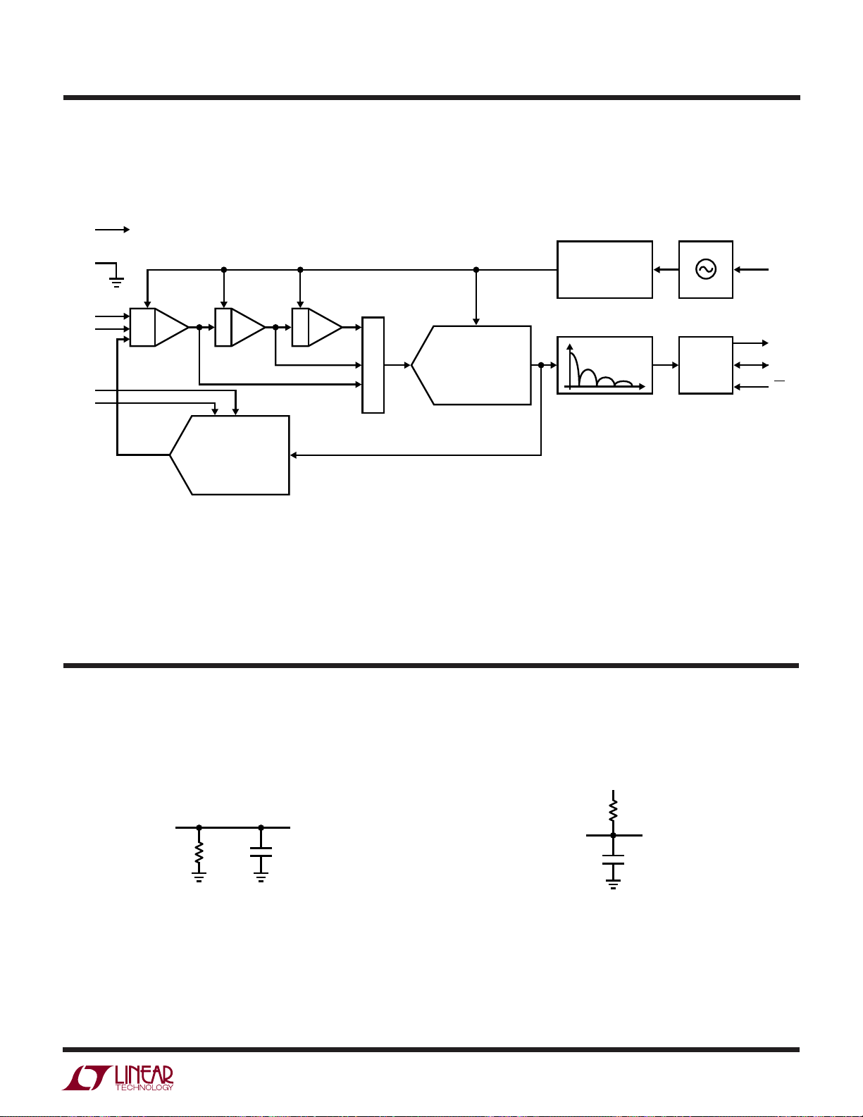
Figure 1. Functional Block Diagram
= 20pF
C
LOAD
OH
2435 TA03
24351fa
11
LTC2435/LTC2435-1
U
WUU
APPLICATIO S I FOR ATIO
CONVERTER OPERATION
Converter Operation Cycle
The LTC2435/LTC2435-1 are low power, delta-sigma analog-to-digital converters with an easy to use 3-wire serial
interface (see Figure 1). Their operation is made up of
three states. The converter operating cycle begins with the
conversion, followed by the sleep state and ends with the
data output (see Figure 2). The 3-wire interface consists of
serial data output (SDO), serial clock (SCK) and chip select
(CS).
CONVERT
SLEEP
There is no latency in the conversion result. The data
output corresponds to the conversion just performed.
This result is shifted out on the serial data out pin (SDO)
under the control of the serial clock (SCK). Data is updated
on the falling edge of SCK allowing the user to reliably latch
data on the rising edge of SCK (see Figure 3). The data
output state is concluded once 24 bits are read out of the
ADC or when CS is brought HIGH. The device automatically initiates a new conversion and the cycle repeats.
Through timing control of the CS and SCK pins, the
LTC2435/LTC2435-1 offer several flexible modes of operation (internal or external SCK and free-running conversion modes). These various modes do not require programming configuration registers; moreover, they do not
disturb the cyclic operation described above. These modes
of operation are described in detail in the Serial Interface
Timing Modes section.
FALSE
CS = LOW
AND
SCK
TRUE
DATA OUTPUT
2435 F02
Figure 2. LTC2435 State Transition Diagram
Initially, the LTC2435/LTC2435-1 perform a conversion.
Once the conversion is complete, the device enters the
sleep state. While in this sleep state, power consumption
is reduced by an order of magnitude if CS is HIGH. The part
remains in the sleep state as long as CS is HIGH. The
conversion result is held indefinitely in a static shift
register while the converter is in the sleep state.
Once CS is pulled LOW, the device exits the low power
sleep mode and enters the data output state. If CS is pulled
HIGH before the first rising edge of SCK, the device returns
to the sleep mode and the conversion result is still held in
the internal static shift register. If CS remains LOW after
the first rising edge of SCK, the device begins outputting
the conversion result. Taking CS HIGH at this point will
terminate the data output state and start a new conversion.
Conversion Clock
A major advantage the delta-sigma converter offers over
conventional type converters is an on-chip digital filter
(commonly implemented as a Sinc or Comb filter). For
high resolution, low frequency applications, this filter is
typically designed to reject line frequencies of 50Hz or
60Hz plus their harmonics. The filter rejection performance is directly related to the accuracy of the converter
system clock. The LTC2435/LTC2435-1 incorporate a
highly accurate on-chip oscillator. This eliminates the
need for external frequency setting components such as
crystals or oscillators. Clocked by the on-chip oscillator,
the LTC2435 achieves a minimum of 110dB rejection at
the line frequency (50Hz or 60Hz ±2%), while the
LTC2435-1 achieves a minimum of 87db rejection at 50Hz
±2% and 60Hz ±2% simultaneously.
Ease of Use
The
LTC2435/LTC2435-1
data output has no latency,
filter settling delay or redundant data associated with the
conversion cycle. There is a one-to-one correspondence
between the conversion and the output data. Therefore,
multiplexing multiple analog voltages is easy.
12
24351fa

LTC2435/LTC2435-1
U
WUU
APPLICATIO S I FOR ATIO
The LTC2435/LTC2435-1 perform a full-scale calibration
every conversion cycle. This calibration is transparent to
the user and has no effect on the cyclic operation described above. The advantage of continuous calibration is
extreme stability of full-scale readings with respect to time,
supply voltage change and temperature drift.
Unlike the LTC2430, the LTC2435 and LTC2435-1 do not
perform an offset calibration every conversion cycle. This
enables the LTC2435/LTC2435-1 to double their output
rate while maintaining line frequency rejection. The initial
offset of the LTC2435/LTC2435-1 is within 5mV independent of V
lator architecture, the temperature drift of the offset is less
than 100nV/°C. More information on the LTC2435/
LTC2435-1 offset is described in the Offset Accuracy and
Drift section of this data sheet.
Power-Up Sequence
The LTC2435/LTC2435-1 automatically enter an internal
reset state when the power supply voltage VCC drops
below approximately 2.2V. This feature guarantees the
integrity of the conversion result and of the serial interface
mode selection. (See the 2-wire I/O sections in the Serial
Interface Timing Modes section.)
When the VCC voltage rises above this critical threshold,
the converter creates an internal power-on-reset (POR)
signal with a duration of approximately 1ms. The POR
signal clears all internal registers. Following the POR
signal, the LTC2435/LTC2435-1 start a normal conversion
cycle and follow the succession of states described above.
The first conversion result following POR is accurate
within the specifications of the device if the power supply
voltage is restored within the operating range (2.7V to
5.5V) before the end of the POR time interval.
Reference Voltage Range
These converters accept a truly differential external reference voltage. The absolute/common mode voltage specification for the REF+ and REF– pins covers the entire range
from GND to VCC. For correct converter operation, the
REF+ pin must always be more positive than the REF– pin.
. Based on the LTC2435/LTC2435-1 new modu-
REF
The LTC2435/LTC2435-1 can accept a differential reference voltage from 0.1V to VCC. The converter output noise
is determined by the thermal noise of the front-end circuits, and as such, its value is nearly constant with
reference voltage. A decrease in reference voltage will not
significantly improve the converter’s effective resolution.
On the other hand, a reduced reference voltage will improve the converter’s overall INL performance. A reduced
reference voltage will also improve the converter performance when operated with an external conversion clock
(external FO signal) at substantially higher output data
rates (see the Output Data Rate section).
Input Voltage Range
The analog input is truly differential with an absolute/
common mode range for the IN+ and IN– input pins
extending from GND – 0.3V to VCC + 0.3V. Outside
these limits, the ESD protection devices begin to turn on
and the errors due to input leakage current increase
rapidly. Within these limits, the LTC2435/LTC2435-1 convert the bipolar differential input signal, VIN = IN+ – IN–,
from –FS = – 0.5 • V
REF+ – REF–. Outside this range, the converters indicate
the overrange or the underrange condition using distinct
output codes.
Input signals applied to IN+ and IN– pins may extend by
300mV below ground and above VCC. In order to limit any
fault current, resistors of up to 5k may be added in series
with the IN+ and IN– pins without affecting the performance of the device. In the physical layout, it is important
to maintain the parasitic capacitance of the connection
between these series resistors and the corresponding pins
as low as possible; therefore, the resistors should be
located as close as practical to the pins. The effect of the
series resistance on the converter accuracy can be evaluated from the curves presented in the Input Current/
Reference Current sections. In addition, series resistors
will introduce a temperature dependent offset error due to
the input leakage current. A 1nA input leakage current will
develop a 1ppm offset error on a 5k resistor if V
This error has a very strong temperature dependency.
to +FS = 0.5 • V
REF
where V
REF
REF
=
REF
= 5V.
24351fa
13

LTC2435/LTC2435-1
U
WUU
APPLICATIO S I FOR ATIO
Output Data Format
The LTC2435/LTC2435-1 serial output data stream is 24
bits long. The first 3 bits represent status information
indicating the sign and conversion state. The next 21 bits
are the conversion result, MSB first. The third and fourth
bit together are also used to indicate an underrange
condition (the differential input voltage is below –FS) or an
overrange condition (the differential input voltage is above
+FS).
Bit 23 (first output bit) is the end of conversion (EOC)
indicator. This bit is available at the SDO pin during the
conversion and sleep states whenever the CS pin is LOW.
This bit is HIGH during the conversion and goes LOW
when the conversion is complete.
Bit 22 (second output bit) is a dummy bit (DMY) and is
always LOW.
Bit 21 (third output bit) is the conversion result sign indicator (SIG). If VIN is >0, this bit is HIGH. If VIN is <0, this
bit is LOW.
Bit 20 (fourth output bit) is the most significant bit (MSB)
of the result. This bit in conjunction with Bit 21 also
provides the underrange or overrange indication. If both
Bit 21 and Bit 20 are HIGH, the differential input voltage is
above +FS. If both are LOW, the differential input voltage
is below –FS.
The function of these bits is summarized in Table 1.
Table 1. LTC2435/LTC2435-1 Status Bits
Bit 23 Bit 22 Bit 21 Bit 20
Input Range EOC DMY SIG MSB
VIN ≥ 0.5 • V
0V ≤ VIN < 0.5 • V
–0.5 • V
VIN < –0.5 • V
REF
REF
≤ VIN < 0V 0 0 0 1
REF
REF
Bits 20-0 are the 21-bit conversion result MSB first.
0011
0010
0000
SCK clock pulses are ignored by the internal data out shift
register.
In order to shift the conversion result out of the device, CS
must first be driven LOW. EOC is seen at the SDO pin of the
device once CS is pulled LOW. EOC changes real time from
HIGH to LOW at the completion of a conversion. This
signal may be used as an interrupt for an external
microcontroller. Bit 23 (EOC) can be captured on the first
rising edge of SCK. Bit 22 is shifted out of the device on the
first falling edge of SCK. The final data bit (Bit 0) is shifted
out on the falling edge of the 23rd SCK and may be latched
on the rising edge of the 24th SCK pulse. On the falling
edge of the 24th SCK pulse, SDO goes HIGH indicating the
initiation of a new conversion cycle. This bit serves as EOC
(Bit 23) for the next conversion cycle. Table 2 summarizes
the output data format.
As long as the voltage on the IN+ and IN– pins is maintained
within the –0.3V to (VCC + 0.3V) absolute maximum
operating range, a conversion result is generated for any
differential input voltage VIN from –FS = –0.5 • V
+FS = 0.5 • V
. For differential input voltages greater
REF
REF
to
than +FS, the conversion result is clamped to the value
corresponding to the +FS. For differential input voltages
below –FS, the conversion result is clamped to the value
corresponding to –FS – 1LSB.
Offset Accuracy and Drift
Unlike the LTC2430 and most of the LTC2400 family, the
LTC2435/LTC2435-1 do not perform an offset calibration
every cycle. The reason for this is to increase the data output
rate while maintaining line frequency rejection.
While the initial accuracy of the LTC2435/LTC2435-1
offset is within 5mV (see Figure 4), several unique properties of the LTC2435/LTC2435-1 architecture nearly eliminate the drift of the offset error with respect to temperature
and supply.
Bit 0 is the least significant bit (LSB).
Data is shifted out of the SDO pin under control of the serial
clock (SCK), see Figure 3. Whenever CS is HIGH, SDO
remains high impedance and any externally generated
14
As shown in Figure 5, the offset variation with temperature
is less than 3ppm over the complete temperature range of
–50°C to 100°C. This corresponds to a temperature drift
of 0.022ppm/°C.
While the variation in offset with supply voltage is propor-
24351fa

LTC2435/LTC2435-1
VCC and V
REF
(V)
2.5 3.0
OFFSET ERROR (ppm OF V
REF
)
3.5 4.54.0
5.0
5.5
2435 F06
–300
–305
–310
–315
–320
–325
–330
–335
–340
–345
–350
REF+ = V
CC
REF– = GND
V
IN
= 0V
V
INCM
= GND
F
O
= GND
T
A
= 25°C
–
U
WUU
APPLICATIO S I FOR ATIO
tional to VCC (see Figure 4), several characteristics of this
variation can be used to eliminate the effects. First, the
variation with respect to supply voltage is linear. Second,
the magnitude of the offset error decreases with decreased supply voltage. Third, the offset error in microvolts is almost independent with reference and therefore
Table 2. LTC2435/LTC2435-1 Output Data Format
Differential Input Voltage Bit 23 Bit 22 Bit 21 Bit 20 Bit 19 Bit 18 Bit 17 … Bit 0
* EOC DMY SIG MSB
V
IN
VIN* ≥ 0.5 • V
0.5 • V
REF
0.25 • V
0.25 • V
0 00100 0 0…0
–1LSB 0 0011 1 1…1
–0.25 • V
–0.25 • V
–0.5 • V
VIN* < –0.5 • V
*The differential input voltage VIN = IN+ – IN–. **The differential reference voltage V
** 0 0110 0 0…0
REF
** – 1LSB 0 0101 1 1…1
** 0 0101 0 0…0
REF
** – 1LSB 0 0100 1 1…1
REF
** 0 0011 0 0…0
REF
** – 1LSB 00010 1 1…1
REF
** 0 0010 0 0…0
REF
** 00001 1 1…1
REF
the offset in ppm is inverse proportional to reference
voltage. As a result, by tying VCC to V
, the variation with
REF
supply can be reduced, see Figure 6. The variation with
supply is less than 15ppm over the entire 2.7V to 5.5V
supply range.
Frequency Rejection Selection LTC2435 (FO)
= REF+ – REF–.
REF
–350
–400
)
REF
–450
–500
–550
–600
–650
OFFSET ERROR (ppm OF V
–700
–750
2.5 3.0
CS
BIT 23
SDO
Hi-Z
SCK
SLEEP DATA OUTPUT CONVERSION
EOC
BIT 20BIT 21BIT 22
MSBSIG“0”
BIT 0BIT 19 BIT 5
LSB
Figure 3. Output Data Timing
3.5 4.54.0
VCC (V)
Figure 4. Offset vs V
REF+ = 2.5V
–
= GND
REF
= 0V
V
IN
= GND
V
INCM
= GND
F
O
= 25°C
T
A
5.0
CC
2435 F04
–324
–325
)
REF
–326
–327
–328
OFFSET ERROR (ppm OF V
–329
5.5
–330
–15 15 30 90
–45 –30 0
TEMPERATURE (°C)
Figure 5. Offset vs Temperature Figure 6. Offset vs VCC (V
VCC = 5V
= 5V
V
REF
= 0V
V
IN
= GND
V
INCM
= GND
F
O
45 60 75
2435 F05
2435 F03
REF
= VCC)
24351fa
15

LTC2435/LTC2435-1
U
WUU
APPLICATIO S I FOR ATIO
The LTC2435 internal oscillator provides better than 110dB
normal mode rejection at the line frequency and its harmonics for 50Hz ±2% or 60Hz ±2%. For 60Hz rejection, F
should be connected to GND while for 50Hz rejection the F
pin should be connected to VCC.
The selection of 50Hz or 60Hz rejection can also be made by
driving FO to an appropriate logic level. A selection change
during the sleep or data output states will not disturb the
converter operation. If the selection is made during the
conversion state, the result of the conversion in progress
may be outside specifications but the following conversions will not be affected.
When a fundamental rejection frequency different from
50Hz or 60Hz is required or when the converter must be
synchronized with an outside source, the LTC2435 can
operate with an external conversion clock. The converter
automatically detects the presence of an external clock
signal at the FO pin and turns off the internal oscillator. The
frequency f
to be detected. The external clock signal duty cycle is not
significant as long as the minimum and maximum specifications for the high and low periods t
observed.
While operating with an external conversion clock of a
frequency f
normal mode rejection in a frequency range f
±4% and its harmonics. The normal mode rejection as a
function of the input frequency deviation from f
is shown in Figure 7a.
Whenever an external clock is not present at the FO pin, the
converter automatically activates its internal oscillator and
enters the Internal Conversion Clock mode. The LTC2435
operation will not be disturbed if the change of conversion
clock source occurs during the sleep state or during the
data output state while the converter uses an external serial
clock. If the change occurs during the conversion state, the
result of the conversion in progress may be outside specifications but the following conversions will not be affected.
of the external signal must be at least 5kHz
EOSC
and t
HEO
, the LTC2435 provides better than 110dB
EOSC
EOSC
EOSC
LEO
/2560
/2560
O
O
are
If the change occurs during the data output state and the
converter is in the Internal SCK mode, the serial clock duty
cycle may be affected but the serial data stream will remain
valid.
Table 3a summarizes the duration of each state and the
achievable output data rate as a function of FO.
Frequency Rejection Selection LTC2435-1 (FO)
The LTC2435-1 internal oscillator provides better than
87dB normal mode rejection over the range of 49Hz to
61.2Hz as shown in Figure 7b. For simultaneous 50Hz/60Hz
rejection, F
In order to achieve 87dB normal mode rejection of 50Hz
±2% and 60Hz ±2%, two consecutive conversions must be
averaged. By performing a continuous running average of
the two most current results, both simultaneous rejection
is achieved and a nearly 2× increase in throughput is
realized relative to the LTC2430 (see Normal Mode Rejection, Ouput Rate and Running Averages sections of this
data sheet).
When a fundamental rejection frequency different from
the range 49Hz to 61.2Hz is required or when the converter
must be synchronized with an outside source, the
LTC2435-1 can operate with an external conversion clock.
The performance of the LTC2435-1 is the same as the
LTC2435 when driven by an external conversion clock at
the FO pin.
Table 3b summarizes the duration of each state and the
achievable output data rate as a function of FO.
Serial Interface Pins
The LTC2435/LTC2435-1 transmit the conversion results
and receive the start of conversion command through a
synchronous 3-wire interface. During the conversion and
sleep states, this interface can be used to assess the
converter status and during the data output state it is used
to read the conversion result.
should be connected to GND.
O
16
24351fa

LTC2435/LTC2435-1
U
WUU
APPLICATIO S I FOR ATIO
–60
–70
–80
–90
–100
–110
REJECTION (dB)
–120
–130
–140
–12–8–404812
INPUT FREQUENCY DEVIATION FROM NOTCH FREQUENCY (%)
2435 F07a
Figure 7a. LTC2435/LTC2435-1 Normal Mode
Rejection When Using an External Oscillator
of Frequency f
without Running Averages
EOSC
–80
–90
–100
–100
–120
–130
NORMAL MODE REECTION RATIO (dB)
–140
48 50 52 54 56 58 60 62
DIFFERENTIAL INPUT SIGNAL FREQUENCY (Hz)
2435 F07b
Figure 7b. LTC2435-1 Normal Mode
Rejection When Using an Internal
Oscillator with Running Averages
–80
–85
–90
–95
–100
–105
–110
–115
–120
–125
NORMAL MODE REJECTION (dB)
–130
–135
–140
–12 –8 –4 0 4 8 12
DIFFERENTIAL INPUT SIGNAL FREQUENCY
DEVIATION FROM NOTCH FREQUENCY f
Figure 7c. LTC2435/LTC2435-1
Normal Mode Rejection When Using
an External Oscillator of Frequency
f
with Running Averages
EOSC
EOSC
/2560(%)
2435 F07c
Table 3a. LTC2435 State Duration
State Operating Mode Duration
CONVERT Internal Oscillator FO = LOW, (60Hz Rejection) 67ms, Output Data Rate ≤ 15 Readings/s
FO = HIGH, (50Hz Rejection) 80ms, Output Data Rate ≤ 12.4 Readings/s
External Oscillator FO = External Oscillator with Frequency 10278/f
f
EOSC
kHz (f
/2560 Rejection)
EOSC
s, Output Data Rate ≤ f
EOSC
/10278 Readings/s
EOSC
SLEEP As Long As CS = HIGH
DATA OUTPUT Internal Serial Clock FO = LOW/HIGH, (Internal Oscillator) As Long As CS = LOW But Not Longer Than 1.25ms (24 SCK cycles)
FO = External Oscillator with As Long As CS = LOW But Not Longer Than 192/f
Frequency f
EOSC
External Serial Clock with Frequency f
kHz
kHz As Long As CS = LOW But Not Longer Than 24/f
SCK
ms (24 SCK cycles)
EOSC
ms (24 SCK cycles)
SCK
Table 3b. LTC2435-1 State Duration
State Operating Mode Duration
CONVERT Internal Oscillator FO = LOW 73ms, Output Data Rate ≤ 14 Readings/s
Simultaneous 50Hz/60Hz Rejection
External Oscillator FO = External Oscillator with Frequency 10278/f
f
EOSC
kHz (f
/2560 Rejection)
EOSC
SLEEP As Long As CS = HIGH
DATA OUTPUT Internal Serial Clock FO = LOW (Internal Oscillator) As Long As CS = LOW But Not Longer Than 1.4ms (24 SCK cycles)
FO = External Oscillator with As Long As CS = LOW But Not Longer Than 192/f
Frequency f
External Serial Clock with Frequency f
kHz
EOSC
kHz As Long As CS = LOW But Not Longer Than 24/f
SCK
s, Output Data Rate ≤ f
EOSC
/10278 Readings/s
EOSC
ms (24 SCK cycles)
EOSC
ms (24 SCK cycles)
SCK
24351fa
17

LTC2435/LTC2435-1
U
WUU
APPLICATIO S I FOR ATIO
Serial Clock Input/Output (SCK)
The serial clock signal present on SCK (Pin 13) is used to
synchronize the data transfer. Each bit of data is shifted out
the SDO pin on the falling edge of the serial clock.
In the Internal SCK mode of operation, the SCK pin is an
output and the LTC2435/LTC2435-1 create their own serial clock by dividing the internal conversion clock by 8. In
the External SCK mode of operation, the SCK pin is used
as input. The internal or external SCK mode is selected on
power-up and then reselected every time a HIGH-to-LOW
transition is detected at the CS pin. If SCK is HIGH or floating at power-up or during this transition, the converter
enters the internal SCK mode. If SCK is LOW at power-up
or during this transition, the converter enters the external
SCK mode.
Serial Data Output (SDO)
Chip Select Input (CS)
The active LOW chip select, CS (Pin 11), is used to test the
conversion status and to enable the data output transfer as
described in the previous sections.
In addition, the CS signal can be used to trigger a new
conversion cycle before the entire serial data transfer has
been completed. The LTC2435/LTC2435-1 will abort any
serial data transfer in progress and start a new conversion
cycle anytime a LOW-to-HIGH transition is detected at the
CS pin after the converter has entered the data output state
(i.e., after the first rising edge of SCK occurs with
CS=LOW).
Finally, CS can be used to control the free-running modes
of operation, see Serial Interface Timing Modes section.
Grounding CS will force the ADC to continuously convert
at the maximum output rate selected by FO.
The serial data output pin, SDO (Pin 12), provides the
result of the last conversion as a serial bit stream (MSB
first) during the data output state. In addition, the SDO pin
is used as an end of conversion indicator during the
conversion and sleep states.
When CS (Pin 11) is HIGH, the SDO driver is switched to
a high impedance state. This allows sharing the serial
interface with other devices. If CS is LOW during the
convert or sleep state, SDO will output EOC. If CS is LOW
during the conversion phase, the EOC bit appears HIGH on
the SDO pin. Once the conversion is complete, EOC goes
LOW.
Table 4. LTC2435/LTC2435-1 Interface Timing Modes
SCK Cycle Output and
Configuration Source Control Control Waveforms
External SCK, Single Cycle Conversion External CS and SCK CS and SCK Figures 8, 9
External SCK, 2-Wire I/O External SCK SCK Figure 10
Internal SCK, Single Cycle Conversion Internal CS ↓ CS ↓ Figures 11, 12
Internal SCK, 2-Wire I/O, Continuous Conversion Internal Continuous Internal Figure 13
SERIAL INTERFACE TIMING MODES
The LTC2435/LTC2435-1 3-wire interface is SPI and
MICROWIRE compatible. This interface offers several
flexible modes of operation. These include internal/external serial clock, 2- or 3-wire I/O, single cycle conversion
and autostart. The following sections describe each of
these serial interface timing modes in detail. In all these
cases, the converter can use the internal oscillator (FO =
LOW or FO = HIGH) or an external oscillator connected to
the FO pin. Refer to Table 4 for a summary.
Conversion Data Connection
18
24351fa

LTC2435/LTC2435-1
U
WUU
APPLICATIO S I FOR ATIO
External Serial Clock, Single Cycle Operation
(SPI/MICROWIRE Compatible)
This timing mode uses an external serial clock to shift out
the conversion result and a CS signal to monitor and
control the state of the conversion cycle, see Figure 8.
The serial clock mode is selected on the falling edge of CS.
To select the external serial clock mode, the serial clock pin
(SCK) must be LOW during each CS falling edge.
The serial data output pin (SDO) is Hi-Z as long as CS is
HIGH. At any time during the conversion cycle, CS may be
pulled LOW in order to monitor the state of the converter.
While CS is pulled LOW, EOC is output to the SDO pin.
EOC = 1 while a conversion is in progress and EOC = 0 if
the conversion is over. With CS HIGH, the device automatically enters the sleep state once the conversion is
complete.
When CS is low, the devcice enters the data output mode.
The result is held in the internal static shift register until
the first SCK rising edge is seen while CS is LOW. Data is
shifted out the SDO pin on each falling edge of SCK. This
enables external circuitry to latch the output on the rising
edge of SCK. EOC can be latched on the first rising edge
of SCK and the last bit of the conversion result can be
latched on the 24th rising edge of SCK. On the 24th falling
edge of SCK, the device begins a new conversion. SDO
goes HIGH (EOC = 1) indicating a conversion is in progress.
At the conclusion of the data cycle, CS may remain LOW
and EOC monitored as an end-of-conversion interrupt.
Alternatively, CS may be driven HIGH setting SDO to Hi-Z.
As described above, CS may be pulled LOW at any time in
order to monitor the conversion status.
Typically, CS remains LOW during the data output state.
However, the data output state may be aborted by pulling
CS HIGH anytime between the first rising edge and the
24th falling edge of SCK, see Figure 9. On the rising edge
of CS, the device aborts the data output state and immediately initiates a new conversion. This is useful for systems not requiring all 24 bits of output data, aborting an
invalid conversion cycle or synchronizing the start of a
conversion.
External Serial Clock, 2-Wire I/O
This timing mode utilizes a 2-wire serial I/O interface. The
conversion result is shifted out of the device by an externally generated serial clock (SCK) signal, see Figure 10. CS
may be permanently tied to ground, simplifying the user
interface or isolation barrier.
SDO
SCK
(EXTERNAL)
CS
TEST EOC
CONVERSION
SLEEP
SLEEP
TEST EOC
BIT 23
EOC
2.7V TO 5.5V
1µF
REFERENCE
VOLTAGE
0.1V TO V
ANALOG INPUT RANGE
TO 0.5V
–0.5V
REF
1, 7, 8, 9, 10, 15, 16
214
V
F
CC
O
LTC2435/
LTC2435-1
3
+
REF
4
REF
CC
5
+
IN
REF
6
–
IN
GND
13
SCK
–
12
SDO
11
CS
DATA OUTPUT CONVERSION
V
CC
= 50Hz REJECTION (LTC2435)
= EXTERNAL OSCILLATOR
= 60Hz REJECTION (LTC2435)
= 50Hz/60Hz REJECTION (LTC2435-1)
3-WIRE
SPI INTERFACE
Figure 8. External Serial Clock, Single Cycle Operation
BIT 0BIT 5BIT 19 BIT 18BIT 20BIT 21BIT 22
LSBMSBSIG
TEST EOC
Hi-ZHi-ZHi-Z
2435 F08
24351fa
19
LTC2435/LTC2435-1
U
WUU
APPLICATIO S I FOR ATIO
ANALOG INPUT RANGE
–0.5V
REF
1, 7, 8, 9, 10, 15, 16
CS
TEST EOC
SDO
SCK
(EXTERNAL)
DATA OUTPUT
EOC
CONVERSIONSLEEP
SLEEP
TEST EOC
Hi-Z
Hi-Z Hi-ZHi-Z
2.7V TO 5.5V
1µF
REFERENCE
VOLTAGE
0.1V TO V
TO 0.5V
BIT 23BIT 0
EOC
SLEEP
214
REF
V
3
REF
4
REF
CC
5
IN
6
IN
GND
CC
LTC2435/
LTC2435-1
+
–
+
–
SCK
SDO
F
O
13
12
11
CS
3-WIRE
SPI INTERFACE
MSBSIG
DATA OUTPUT
V
CC
= 50Hz REJECTION (LTC2435)
= EXTERNAL OSCILLATOR
= 60Hz REJECTION (LTC2435)
= 50Hz/60Hz REJECTION (LTC2435-1)
BIT 8BIT 19 BIT 9BIT 20BIT 21BIT 22
TEST EOC
CONVERSION
2435 F09
Figure 9. External Serial Clock, Reduced Data Output Length
The external serial clock mode is selected at the end of the
power-on reset (POR) cycle. The POR cycle is concluded
approximately 1ms after VCC exceeds 2.2V. The level
applied to SCK at this time determines if SCK is internal or
external. SCK must be driven LOW prior to the end of POR
in order to enter the external serial clock timing mode.
Since CS is tied LOW, the end-of-conversion (EOC) can be
continuously monitored at the SDO pin during the convert
and sleep states. EOC may be used as an interrupt to an
external controller indicating the conversion result is
ready. EOC = 1 while the conversion is in progress and
EOC = 0 once the conversion is over. On the falling edge of
EOC, the conversion result is loaded into an internal static
shift register. Data is shifted out the SDO pin on each
falling edge of SCK enabling external circuitry to latch data
on the rising edge of SCK. EOC can be latched on the first
rising edge of SCK. On the 24th falling edge of SCK, SDO
goes HIGH (EOC = 1) indicating a new conversion has
begun.
Internal Serial Clock, Single Cycle Operation
This timing mode uses an internal serial clock to shift out
the conversion result and a CS signal to monitor and
control the state of the conversion cycle, see Figure 11.
In order to select the internal serial clock timing mode, the
serial clock pin (SCK) must be floating (Hi-Z) or pulled
HIGH prior to the falling edge of CS. The device will not
enter the internal serial clock mode if SCK is driven LOW
on the falling edge of CS. An internal weak pull-up resistor
is active on the SCK pin during the falling edge of CS;
therefore, the internal serial clock timing mode is automatically selected if SCK is not externally driven.
The serial data output pin (SDO) is Hi-Z as long as CS is
HIGH. At any time during the conversion cycle, CS may be
pulled LOW in order to monitor the state of the converter.
Once CS is pulled LOW, SCK goes LOW and EOC is output
to the SDO pin. EOC = 1 while a conversion is in progress
and EOC = 0 if the conversion is over.
20
24351fa

LTC2435/LTC2435-1
U
WUU
APPLICATIO S I FOR ATIO
When testing EOC, if the conversion is complete (EOC = 0),
the device will exit the sleep state and enter the data output
state. In order to allow the device to return to the sleep
state, CS must be pulled HIGH before the first rising edge
of SCK. In the internal SCK timing mode, SCK goes HIGH
2.7V TO 5.5V
1µF
214
3
4
CC
5
REF
6
MSB LSBSIG
SDO
REFERENCE
VOLTAGE
0.1V TO V
ANALOG INPUT RANGE
TO 0.5V
–0.5V
REF
1, 7, 8, 9, 10, 15, 16
CS
BIT 23
EOC
and the device begins outputting data at time t
the falling edge of CS (if EOC = 0) or t
after EOC goes
EOCtest
EOCtest
after
LOW (if CS is LOW during the falling edge of EOC). The
value of t
is 23µs (LTC2435), 26µs (LTC2435-1) if
EOCtest
the device is using its internal oscillator (F0 = logic LOW or
V
CC
= 50Hz REJECTION (LTC2435)
V
CC
LTC2435/
LTC2435-1
+
REF
–
REF
+
IN
–
IN
GND
SCK
SDO
F
O
13
12
11
CS
= EXTERNAL OSCILLATOR
= 60Hz REJECTION (LTC2435)
= 50Hz/60Hz REJECTION (LTC2435-1)
2-WIRE
INTERFACE
BIT 0BIT 5BIT 19 BIT 18BIT 20BIT 21BIT 22
SCK
(EXTERNAL)
SDO
SCK
(INTERNAL)
CS
CONVERSION
DATA OUTPUT CONVERSION
Figure 10. External Serial Clock, CS = 0 Operation (2-Wire)
2.7V TO 5.5V
1µF
214
V
REFERENCE
VOLTAGE
0.1V TO V
ANALOG INPUT RANGE
TO 0.5V
–0.5V
REF
1, 7, 8, 9, 10, 15, 16
<t
EOCtest
BIT 23
Hi-Z Hi-Z Hi-Z Hi-Z
SLEEP
EOC
SLEEP
TEST EOC
3
REF
4
REF
CC
5
IN
REF
6
IN
GND
MSB LSBSIG
CC
LTC2435/
LTC2435-1
+
–
+
–
BIT 19 BIT 18BIT 20BIT 21BIT 22
SCK
SDO
F
O
13
12
11
CS
DATA OUTPUT CONVERSIONCONVERSION
V
CC
= 50Hz REJECTION (LTC2435)
= EXTERNAL OSCILLATOR
= 60Hz REJECTION (LTC2435)
= 50Hz/60Hz REJECTION (LTC2435-1)
3-WIRE
SPI INTERFACE
V
CC
10k
BIT 0BIT 5
Figure 11. Internal Serial Clock, Single Cycle Operation
2435 F10
TEST EOC
2435 F11
24351fa
21

LTC2435/LTC2435-1
U
WUU
APPLICATIO S I FOR ATIO
HIGH). If FO is driven by an external oscillator of frequency
f
, then t
EOSC
time t
EOCtest
conversion result is held in the internal static shift register.
If CS remains LOW longer than t
edge of SCK will occur and the conversion result is serially
shifted out of the SDO pin. The data output cycle begins on
this first rising edge of SCK and concludes after the 24th
rising edge. Data is shifted out the SDO pin on each falling
edge of SCK. The internally generated serial clock is output
to the SCK pin. This signal may be used to shift the
conversion result into external circuitry. EOC can be
latched on the first rising edge of SCK and the last bit of the
conversion result on the 24th rising edge of SCK. After the
24th rising edge, SDO goes HIGH (EOC = 1), SCK stays
HIGH and a new conversion starts.
Typically, CS remains LOW during the data output state.
However, the data output state may be aborted by pulling
CS HIGH anytime between the first and 24th rising edge of
SCK, see Figure 12. On the rising edge of CS, the device
aborts the data output state and immediately initiates a
EOCtest
is 3.6/f
. If CS is pulled HIGH before
EOSC
, the device returns to the sleep state. The
, the first rising
EOCtest
new conversion. This is useful for systems not requiring
all 24 bits of output data, aborting an invalid conversion
cycle, or synchronizing the start of a conversion. If CS is
pulled HIGH while the converter is driving SCK LOW, the
internal pull-up is not available to restore SCK to a logic
HIGH state. This will cause the device to exit the internal
serial clock mode on the next falling edge of CS. This can
be avoided by adding an external 10k pull-up resistor to
the SCK pin or by never pulling CS HIGH when SCK is LOW.
Whenever SCK is LOW, the LTC2435/LTC2435-1 internal
pull-up at pin SCK is disabled. Normally, SCK is not
externally driven if the device is in the internal SCK timing
mode. However, certain applications may require an external driver on SCK. If this driver goes Hi-Z after outputting
a LOW signal, the LTC2435/LTC2435-1 internal pull-up
remains disabled. Hence, SCK remains LOW. On the next
falling edge of CS, the device is switched to the external
SCK timing mode. By adding an external 10k pull-up
resistor to SCK, this pin goes HIGH once the external driver
goes Hi-Z. On the next CS falling edge, the device will
remain in the internal SCK timing mode.
SDO
SCK
(INTERNAL)
DATA OUTPUT
2.7V TO 5.5V
1µF
214
V
REF
3
REF
4
REF
CC
5
IN
6
IN
GND
REFERENCE
VOLTAGE
0.1V TO V
ANALOG INPUT RANGE
TO 0.5V
–0.5V
REF
1, 7, 8, 9, 10, 15, 16
>t
EOCtest
CS
BIT 0
EOC
Hi-Z Hi-Z Hi-Z Hi-Z Hi-Z
TEST EOC
SLEEP
SLEEP
<t
EOCtest
BIT 23
EOC
TEST EOC
CC
LTC2435/
LTC2435-1
+
–
+
–
SCK
SDO
F
O
CS
13
12
11
DATA OUTPUT
MSBSIG
V
CC
= 50Hz REJECTION (LTC2435)
= EXTERNAL OSCILLATOR
= 60Hz REJECTION (LTC2435)
= 50Hz/60Hz REJECTION (LTC2435-1)
3-WIRE
SPI INTERFACE
BIT 19 BIT 18BIT 20BIT 21BIT 22
BIT 8
Figure 12. Internal Serial Clock, Reduced Data Output Length
V
CONVERSIONCONVERSIONSLEEP
CC
10k
TEST EOC
2435 F12
24351fa
22

LTC2435/LTC2435-1
U
WUU
APPLICATIO S I FOR ATIO
A similar situation may occur during the sleep state when
CS is pulsed HIGH-LOW-HIGH in order to test the conversion status. If the device is in the sleep state (EOC = 0), SCK
will go LOW. Once CS goes HIGH (within the time period
defined above as t
For a heavy capacitive load on the SCK pin, the internal
pull-up may not be adequate to return SCK to a HIGH level
before CS goes low again. This is not a concern under
normal conditions where CS remains LOW after detecting
EOC = 0. This situation is easily overcome by adding an
external 10k pull-up resistor to the SCK pin.
Internal Serial Clock, 2-Wire I/O,
Continuous Conversion
This timing mode uses a 2-wire, all output (SCK and SDO)
interface. The conversion result is shifted out of the device
by an internally generated serial clock (SCK) signal, see
Figure 13. CS may be permanently tied to ground, simplifying the user interface or isolation barrier.
The internal serial clock mode is selected at the end of the
power-on reset (POR) cycle. The POR cycle is concluded
), the internal pull-up is activated.
EOCtest
approximately 1ms after VCC exceeds 2.2V. An internal
weak pull-up is active during the POR cycle; therefore, the
internal serial clock timing mode is automatically selected
if SCK is not externally driven LOW (if SCK is loaded such
that the internal pull-up cannot pull the pin HIGH, the
external SCK mode will be selected).
During the conversion, the SCK and the serial data output
pin (SDO) are HIGH (EOC = 1). Once the conversion is
complete, SCK and SDO go LOW (EOC = 0) indicating the
conversion has finished. The data output cycle begins on
the first rising edge of SCK and ends after the 24th rising
edge. Data is shifted out the SDO pin on each falling edge
of SCK. The internally generated serial clock is output to
the SCK pin. This signal may be used to shift the conversion result into external circuitry. EOC can be latched on
the first rising edge of SCK and the last bit of the
conversion result can be latched on the 24th rising edge
of SCK. After the 24th rising edge, SDO goes HIGH (EOC
= 1) indicating a new conversion is in progress. SCK
remains HIGH during the conversion.
SDO
SCK
(INTERNAL)
2.7V TO 5.5V
1µF
214
V
CC
REF
3
REF
4
REF
CC
5
IN
6
IN
GND
REFERENCE
VOLTAGE
0.1V TO V
ANALOG INPUT RANGE
CS
BIT 23
EOC
TO 0.5V
–0.5V
REF
1, 7, 8, 9, 10, 15, 16
LTC2435/
LTC2435-1
+
–
+
–
DATA OUTPUT CONVERSIONCONVERSION
SCK
SDO
F
O
13
12
11
CS
V
CC
= 50Hz REJECTION (LTC2435)
= EXTERNAL OSCILLATOR
= 60Hz REJECTION (LTC2435)
= 50Hz/60Hz REJECTION (LTC2435-1)
2-WIRE
INTERFACE
BIT 5 BIT 0BIT 19 BIT 18BIT 20BIT 21BIT 22
LSBMSBSIG
2435 F13
Figure 13. Internal Serial Clock, Continuous Operation
24351fa
23

LTC2435/LTC2435-1
U
WUU
APPLICATIO S I FOR ATIO
PRESERVING THE CONVERTER ACCURACY
The LTC2435/LTC2435-1 are designed to reduce as much
as possible conversion result sensitivity to device
decoupling, PCB layout, antialiasing circuits, line frequency perturbations and so on. Nevertheless, in order to
preserve the extreme accuracy capability of this part,
some simple precautions are desirable.
Digital Signal Levels
The LTC2435/LTC2435-1 digital interface is easy to use.
Its digital inputs (FO, CS and SCK in External SCK mode of
operation) accept standard TTL/CMOS logic levels and the
internal hysteresis receivers can tolerate edge rates as slow
as 100µs. However, some considerations are required to
take advantage of the exceptional accuracy and low supply
current of this converter.
The digital output signals (SDO and SCK in Internal SCK
mode of operation) are less of a concern because they are
not generally active during conversion.
While a digital input signal is in the range 0.5V to
(VCC– 0.5V), the CMOS input receiver draws additional
current from the power supply. It should be noted that,
when any one of the digital input signals (FO, CS and SCK
in External SCK mode of operation) is within this range, the
LTC2435/LTC2435-1 power supply current may increase
even if the signal in question is at a valid logic level. For
micropower operation, it is recommended to drive all
digital input signals to full CMOS levels [VIL < 0.4V and
VOH > (VCC – 0.4V)].
During the conversion period, the undershoot and/or
overshoot of a fast digital signal connected to the LTC2435/
LTC2435-1 pins may severely disturb the analog to digital
conversion process. Undershoot and overshoot can occur because of the impedance mismatch at the converter
pin when the transition time of an external control signal
is less than twice the propagation delay from the driver to
LTC2435/LTC2435-1. For reference, on a regular FR-4
board, signal propagation velocity is approximately
183ps/inch for internal traces and 170ps/inch for surface
traces. Thus, a driver generating a control signal with a
minimum transition time of 1ns must be connected to the
converter pin through a trace shorter than 2.5 inches. This
problem becomes particularly difficult when shared control lines are used and multiple reflections may occur. The
solution is to carefully terminate all transmission lines
close to their characteristic impedance.
Parallel termination near the
will eliminate this problem but will increase the driver
power dissipation. A series resistor between 27Ω and 56Ω
placed near the driver or near the
pins will also eliminate this problem without additional
power dissipation. The actual resistor value depends upon
the trace impedance and connection topology.
An alternate solution is to reduce the edge rate of the
control signals. It should be noted that using very slow
edges will increase the converter power supply current
during the transition time. The multiple ground pins used
in this package configuration, as well as the differential
input and reference architecture, reduce substantially the
converter’s sensitivity to ground currents.
Particular attention must be given to the connection of the
FO signal when the
external conversion clock. This clock is active during the
conversion time and the normal mode rejection provided
by the internal digital filter is not very high at this frequency. A normal mode signal of this frequency at the
converter reference terminals may result in DC gain and
INL errors. A normal mode signal of this frequency at the
converter input terminals may result in a DC offset error.
Such perturbations may occur due to asymmetric capacitive coupling between the FO signal trace and the converter
input and/or reference connection traces. An immediate
solution is to maintain maximum possible separation
between the FO signal trace and the input/reference signals. When the FO signal is parallel terminated near the
converter, substantial AC current is flowing in the loop
formed by the FO connection trace, the termination and the
ground return path. Thus, perturbation signals may be
inductively coupled into the converter input and/or reference. In this situation, the user must reduce to a minimum
the loop area for the FO signal as well as the loop area for
the differential input and reference connections.
LTC2435/LTC2435-1
LTC2435/LTC2435-1
LTC2435/LTC2435-1
are used with an
pins
24
24351fa

LTC2435/LTC2435-1
U
WUU
APPLICATIO S I FOR ATIO
Driving the Input and Reference
The input and reference pins of the
converters are directly connected to a network of sampling
capacitors. Depending upon the relation between the
differential input voltage and the differential reference
voltage, these capacitors are switching between these
four pins transferring small amounts of charge in the
process. A simplified equivalent circuit is shown in
Figure 14.
For a simple approximation, the source impedance R
driving an analog input pin (IN+, IN–, REF+ or REF–) can be
considered to form, together with RSW and CEQ (see
Figure 14), a first order passive network with a time
constant τ = (RS + RSW) • CEQ. The converter is able to
sample the input signal with better than 1ppm accuracy if
the sampling period is at least 14 times greater than the
input circuit time constant τ. The sampling process on the
four input analog pins is quasi-independent so each time
constant should be considered by itself and, under worstcase circumstances, the errors may add.
When using the internal oscillator (FO = LOW or HIGH), the
LTC2435’s front-end switched-capacitor network is clocked
at 76800Hz corresponding to a 13µs sampling period and
the LTC2435-1’s front end is clocked at 69900Hz corresponding to 14.2µs. Thus, for settling errors of less than
1ppm, the driving source impedance should be chosen
such that τ ≤ 13µs/14 = 920ns (LTC2435) and τ <14.2µs/
14 = 1.01µs (LTC2435-1). When an external oscillator of
frequency f
and, for a settling error of less than 1ppm, τ ≤ 0.14/f
Input Current
If complete settling occurs on the input, conversion results will be unaffected by the dynamic input current. An
incomplete settling of the input signal sampling process
may result in gain and offset errors, but it will not degrade
the INL performance of the converter. Figure 14 shows the
mathematical expressions for the average bias currents
flowing through the IN+ and IN– pins as a result of the
sampling charge transfers when integrated over a substantial time period (longer than 64 internal clock cycles).
is used, the sampling period is 2/f
EOSC
LTC2435/LTC2435-1
S
EOSC
EOSC
.
The effect of this input dynamic current can be analyzed
using the test circuit of Figure 15. The C
includes the LTC2435/LTC2435-1 pin capacitance (5pF
typical) plus the capacitance of the test fixture used to
obtain the results shown in Figures 16 and 17. A careful
implementation can bring the total input capacitance (C
+ C
than the one predicted by Figures 16 and 17. For simplicity, two distinct situations can be considered.
For relatively small values of input capacitance (CIN <
0.01µF), the voltage on the sampling capacitor settles
almost completely and relatively large values for the
source impedance result in only small errors. Such values
for C
performance without significant benefits of signal filtering
and the user is advised to avoid them. Nevertheless, when
small values of CIN are unavoidably present as parasitics
of input multiplexers, wires, connectors or sensors, the
LTC2435/LTC2435-1 can maintain their exceptional accuracy while operating with relative large values of source
resistance as shown in Figures 16 and 17. These measured results may be slightly different from the first order
approximation suggested earlier because they include the
effect of the actual second order input network together
with the nonlinear settling process of the input amplifiers.
For small CIN values, the settling on IN+ and IN– occurs
almost independently and there is little benefit in trying to
match the source impedance for the two pins.
Larger values of input capacitors (CIN > 0.01µF) may be
required in certain configurations for antialiasing or general input signal filtering. Such capacitors will average the
input sampling charge and the external source resistance
will see a quasi constant input differential impedance.
When FO = LOW (internal oscillator and 60Hz notch), the
typical differential input resistance is 22MΩ (LTC2435) or
24MΩ (LTC2435-1) which will generate a +FS gain error
of approximately 0.023ppm (LTC2435) or 0.021ppm
(LTC2435-1) for each ohm of source resistance driving
IN+ or IN–. For the LTC2435, when FO = HIGH (internal
oscillator and 50Hz notch), the typical differential input
resistance is 26MΩ which will generate a +FS gain error of
approximately 0.019ppm for each ohm of source resis-
) closer to 5pF thus achieving better performance
PAR
will deteriorate the converter offset and gain
IN
capacitor
PAR
IN
24351fa
25

LTC2435/LTC2435-1
U
WUU
APPLICATIO S I FOR ATIO
V
CC
I
+
V
VIN+
VIN–
I
V
REF
REF
IIN+
IIN–
REF
REF
I
LEAK
+
I
LEAK
V
CC
V
CC
I
LEAK
I
LEAK
V
–
–
CC
I
LEAK
I
LEAK
I
LEAK
I
LEAK
RSW (TYP)
20k
RSW (TYP)
20k
RSW (TYP)
20k
RSW (TYP)
20k
C
EQ
18pF
(TYP)
SWITCHING FREQUENCY
= 76800Hz INTERNAL
f
SW
OSCILLATOR (LTC2435)
= LOW OR HIGH)
(F
O
= 69900Hz INTERNAL
f
SW
OSCILLATOR (LTC2435-1)
= LOW)
(F
O
f
SW
= 0.5 • f
EXTERNAL OSCILLATOR
EOSC
Figure 14. LTC2435/LTC2435-1 Equivalent Analog Input Circuit
2435 F18
VV V
+ −
IN INCM REFCM
+
IIN
=
()
AVG
−
IIN
()
AVG
+
I REF
()
−
I REF
()
::
where
V REF REF
= −
REF
V
REFCM
VININ
= −
IN
V
=
INCM
R
= 43.2MΩ INTERNAL OSCILLATOR 60Hz NOTCH (FO = LOW) LTC2435
EQ
R
= 52MΩ INTERNAL OSCILLATOR 50Hz NOTCH (FO = HIGH) LTC2435
EQ
R
= 48MΩ INTERNAL OSCILLATOR 50Hz/60Hz NOTCH (FO = LOW) LTC2435-1
EQ
R
= (6.7 • 1012)/f
EQ
05
− + −
VV V
IN INCM REFCM
=
• − +
15
.
=
AVG
− • − +
15
.
=
AVG
+ −
+ −
⎛
REF REF
+
=
⎜
2
⎝
+ −
+ −
⎛
IN IN
−
⎜
2
⎝
EOSC
R
•
.
EQ
•
05
R
.
EQ
VV V
REF INCM REFCM
05
R
.
•
EQ
VV V
REF INCM REFCM
•
05
R
.
EQ
⎞
⎟
⎠
⎞
⎟
⎠
EXTERNAL OSCILLATOR
2
V
IN
−
•
VR
REF EQ
V
+
VR
REF EQ
2
IN
•
10
0
–10
–20
–30
–40
–50
V
= 5V
CC
–60
–70
+FS ERROR VARIATION (ppm)
–80
–90
–100
+
= 5V
V
REF
–
= GND
V
REF
+
= 3.75V
V
IN
–
= 1.25V
V
IN
= GND
F
O
= 25°C
T
A
10
1
CIN = 0pF
CIN = 0.01µF
CIN = 0.001µF
CIN = 100pF
100
R
SOURCE
1000
(W)
R
SOURCE
V
V
INCM
INCM
+ 0.5V
– 0.5V
IN
R
SOURCE
IN
C
IN
C
IN
Figure 15. An RC Network at IN+ and IN
10000
100000
2435 F16
+
IN
C
PAR
≅20pF
C
≅20pF
PAR
LTC2435/
LTC2435-1
–
IN
2435 F19
–
100
V
CC
90
V
REF
V
REF
80
V
IN
70
V
IN
= GND
F
O
60
= 25°C
T
A
50
40
30
20
–FS ERROR VARIATION (ppm)
10
0
–10
1
= 5V
+
= 5V
–
= GND
+
= 1.25V
–
= 3.75V
10
CIN = 0.01µF
CIN = 100pF
CIN = 0.001µF
CIN = 0pF
100
R
SOURCE
1000
(W)
10000
100000
2435 F17
Figure 16. +FS Error vs R
26
at IN+ or IN– (Small CIN)
SOURCE
Figure 17. –FS Error vs R
at IN+ or IN– (Small CIN)
SOURCE
24351fa

LTC2435/LTC2435-1
U
WUU
APPLICATIO S I FOR ATIO
tance driving IN+ or IN–. When FO is driven by an external
oscillator with a frequency f
clock operation), the typical differential input resistance is
3.3 • 1012/f
Ω and each ohm of source resistance
EOSC
driving IN+ or IN– will result in 0.15 • 10–6 • f
gain error. The effect of the source resistance on the two
input pins is additive with respect to this gain error. The
typical +FS and –FS errors as a function of the sum of the
source resistance seen by IN
C
are shown in Figures 18 and 19.
IN
In addition to this gain error, an offset error term may also
appear. The offset error is proportional to the mismatch
between the source impedance driving the two input pins
IN+ and IN– and with the difference between the input and
reference common mode voltages. While the input drive
circuit nonzero source impedance combined with the
converter average input current will not degrade the INL
performance, indirect distortion may result from the modulation of the offset error by the common mode component
of the input signal. Thus, when using large CIN capacitor
values, it is advisable to carefully match the source impedance seen by the IN+ and IN– pins. When FO = LOW
(internal oscillator and 60Hz notch), every 1Ω mismatch
in source impedance transforms a full-scale common
mode input signal into a differential mode input signal of
0.023ppm. When FO = HIGH (internal oscillator and 50Hz
(external conversion
EOSC
ppm +FS
EOSC
+
and IN– for large values of
notch), every 1Ω mismatch in source impedance transforms a full-scale common mode input signal into a
differential mode input signal of 0.02ppm. When F
driven by an external oscillator with a frequency f
is
O
EOSC
,
every 1Ω mismatch in source impedance transforms a
full-scale common mode input signal into a differential
mode input signal of 0.15 • 10–6 • f
ppm. Figure 20
EOSC
shows the typical offset error due to input common mode
voltage for various values of source resistance imbalance
between the IN+ and IN– pins when large CIN values are
used.
If possible, it is desirable to operate with the input signal
common mode voltage very close to the reference signal
common mode voltage as is the case in the ratiometric
measurement of a symmetric bridge. This configuration
eliminates the offset error caused by mismatched source
impedances.
The magnitude of the dynamic input current depends upon
the size of the very stable internal sampling capacitors and
upon the accuracy of the converter sampling clock. The
accuracy of the internal clock over the entire temperature
and power supply range is typical better than 0.5%. Such
a specification can also be easily achieved by an external
clock. When relatively stable resistors (50ppm/°C) are
used for the external source impedance seen by IN+ and
IN–, the expected drift of the dynamic current, offset and
0
–10
–20
–30
–40
–50
V
= 5V
CC
–60
–70
–80
+FS ERROR VARIATION (ppm)
–90
–100
+
= 5V
V
REF
–
= GND
V
REF
+
= 3.75V
V
IN
–
= 1.25V
V
IN
= GND
F
O
= 25°C
T
A
0 400
CIN = 1µF, 10µF
800
R
SOURCE
Figure 18. +FS Error vs R
at IN+ or IN– (Large CIN)
CIN = 0.01µF
CIN = 0.1µF
1200 1600 2000
(Ω)
2435 F18
SOURCE
100
V
= 5V
CC
+
90
= 5V
V
REF
–
= GND
V
REF
80
+
= 1.25V
V
IN
–
= 3.75V
V
IN
70
= GND
F
O
60
= 25°C
T
A
50
40
30
20
–FS ERROR VARIATION (ppm)
10
0
0 400
CIN = 1µF, 10µF
800
R
SOURCE
Figure 19. –FS Error vs R
at IN+ or IN– (Large CIN)
CIN = 0.1µF
CIN = 0.01µF
1200 1600 2000
(Ω)
2435 F19
SOURCE
–310
–320
–330
–340
–350
–360
OFFSET ERROR (ppm)
–370
–380
0
A: ∆RIN = 1k
B: ∆R
C: ∆R
D: ∆R
0.5
1.0
IN
IN
IN
V
CC
V
REF
V
REF
V
IN
1.5
Figure 20. Offset Error vs Common Mode
Voltage (V
INCM
= 500Ω
= 200Ω
= 0Ω
= 5V
+
= 5V
–
= GND
+
= V
2.0
= V
IN
V
INCM
IN
–
= V
2.5
+
E: ∆R
F: ∆R
G: ∆R
(V)
= V
= –200Ω
IN
= –500Ω
IN
= –1k
IN
FO = GND
= 25°C
T
A
= 10µF
C
IN
INCM
3.5 4.5
3.0 4.0
–
) and Input
IN
A
B
C
D
E
F
G
5.0
2435 F20
Source Resistance Imbalance (∆RIN =
R
SOURCEIN
+ – R
SOURCEIN
–) for Large C
IN
Values (CIN ≥ 1µF)
24351fa
27

LTC2435/LTC2435-1
U
WUU
APPLICATIO S I FOR ATIO
gain errors will be insignificant (about 1% of their respective values over the entire temperature and voltage range).
Even for the most stringent applications, a one-time
calibration operation may be sufficient.
In addition to the input sampling charge, the input ESD
protection diodes have a temperature dependent leakage
current. This current, nominally 1nA (±10nA max), results
in a small offset shift. A 100Ω source resistance will create
a 0.1µV typical and 1µV maximum offset voltage.
Reference Current
In a similar fashion, the LTC2435/LTC2435-1 sample the
differential reference pins REF+ and REF– transferring
small amount of charge to and from the external driving
circuits thus producing a dynamic reference current. This
current does not change the converter offset, but it may
degrade the gain and INL performance. The effect of this
current can be analyzed in the same two distinct situations.
For relatively small values of the external reference capacitors (C
settles almost completely and relatively large values for
the source impedance result in only small errors. Such
values for C
gain performance without significant benefits of reference
filtering and the user is advised to avoid them.
< 0.01µF), the voltage on the sampling capacitor
REF
will deteriorate the converter offset and
REF
Larger values of reference capacitors (C
> 0.01µF) may
REF
be required as reference filters in certain configurations.
Such capacitors will average the reference sampling charge
and the external source resistance will see a quasi constant reference differential impedance. For the LTC2435,
when F
= LOW (internal oscillator and 60Hz notch), the
O
typical differential reference resistance is 15.6MΩ which
will generate a +FS gain error of approximately 0.032ppm
for each ohm of source resistance driving REF+ or REF–.
When F
= HIGH (internal oscillator and 50Hz notch), the
O
typical differential reference resistance is 18.7MΩ which
will generate a +FS gain error of approximately 0.027ppm
for each ohm of source resistance driving REF+ or REF–.
For the LTC2435-1, the typical differential reference resistance is 17.1MΩ which will generate a +FS gain error of
approximately 0.029ppm for each ohm of source resistance driving REF+ or REF–. When FO is driven by an
external oscillator with a frequency f
(external conver-
EOSC
sion clock operation), the typical differential reference
resistance is 2.4 • 1012/f
Ω and each ohm of source
EOSC
resistance driving REF+ or REF– will result in
0.21 • 10–6 • f
ppm +FS gain error. The effect of the
EOSC
source resistance on the two reference pins is additive
with respect to this gain error. The typical +FS and –FS
errors for various combinations of source resistance seen
by the REF+ and REF– pins and external capacitance C
REF
connected to these pins are shown in Figures 21, 22, 23
and 24.
100
V
CC
90
V
REF
V
REF
80
+
V
IN
–
70
V
IN
= GND
F
O
60
= 25°C
T
A
50
40
30
20
+FS ERROR VARIATION (ppm)
10
0
–10
1
Figure 21. +FS Error vs R
28
= 5V
+
= 5V
–
= GND
= 3.75V
= 1.25V
10
CIN = 0.01µF
CIN = 100pF
CIN = 0.001µF
CIN = 0pF
1000
10000
100
R
(Ω)
SOURCE
at REF+ or REF– (Small CIN) Figure 22. – FS Error vs R
SOURCE
100000
2435 F21
10
0
= 5V
+
= 5V
–
= GND
+
= 1.25V
–
= 3.75V
= GND
= 25°C
10
CIN = 0.01µF
CIN = 0.001µF
CIN = 100pF
100
R
SOURCE
SOURCE
–10
–20
–30
–40
–50
V
CC
–60
V
REF
V
REF
–70
V
IN
–FS ERROR VARIATION (ppm)
–80
V
IN
F
O
–90
T
A
–100
1
CIN = 0pF
1000
10000
100000
(Ω)
2435 F22
at REF+ or REF– (Small CIN)
24351fa

LTC2435/LTC2435-1
U
WUU
APPLICATIO S I FOR ATIO
100
V
= 5V
CC
+
90
= 5V
V
REF
–
= GND
V
REF
80
+
= 3.75V
V
IN
–
= 1.25V
V
IN
70
= GND
F
O
60
T
= 25°C
A
50
40
30
20
+FS ERROR VARIATION (ppm)
10
0
0 400
Figure 23. +FS Error vs R
SOURCE
In addition to this gain error, the converter INL performance is degraded by the reference source impedance.
When FO = LOW (internal oscillator and 60Hz notch), every
100Ω of source resistance driving REF+ or REF– translates
into about 0.11ppm additional INL error. For the LTC2435,
when FO = HIGH (internal oscillator and 50Hz notch), every
100Ω of source resistance driving REF+ or REF– translates
into about 0.092ppm additional INL error; and for the
LTC2435-1 operating with simultaneous 50Hz/60Hz rejection, every 100Ω of source resistance leads to an
additional 0.10ppm of additional INL error. When FO is
driven by an external oscillator with a frequency f
every 100Ω of source resistance driving REF+ or REF
translates into about 0.73 • 10–6 • f
error. Figure 25 shows the typical INL error due to the
source resistance driving the REF+ or REF– pins when
large C
values are used. The effect of the source
REF
resistance on the two reference pins is additive with
respect to this INL error. In general, matching of source
impedance for the REF+ and REF– pins does not help the
gain or the INL error. The user is thus advised to minimize
the combined source impedance driving the REF+ and
REF– pins rather than to try to match it.
The magnitude of the dynamic reference current depends
upon the size of the very stable internal sampling capacitors and upon the accuracy of the converter sampling
clock. The accuracy of the internal clock over the entire
temperature and power supply range is typical better than
0.5%. Such a specification can also be easily achieved by
CIN = 1µF, 10µF
CIN = 0.1µF
CIN = 0.01µF
800
1200 1600 2000
R
(Ω)
SOURCE
2435 F23
at REF+ and REF– (Large C
ppm additional INL
EOSC
REF
EOSC
)
,
–
0
–10
–20
–30
–40
–50
V
= 5V
CC
–60
–70
–80
–FS ERROR VARIATION (ppm)
–90
–100
+
= 5V
V
REF
–
= GND
V
REF
+
= 1.25V
V
IN
–
= 3.75V
V
IN
= GND
F
O
= 25°C
T
A
0 400
Figure 24. –FS Error vs R
CIN = 1µF, 10µF
800
R
SOURCE
SOURCE
CIN = 0.01µF
CIN = 0.1µF
1200 1600 2000
(Ω)
2435 F24
at REF+ and REF– (Large C
REF
)
an external clock. When relatively stable resistors
(50ppm/°C) are used for the external source impedance
seen by REF+ and REF–, the expected drift of the dynamic
current gain error will be insignificant (about 1% of its
value over the entire temperature and voltage range). Even
for the most stringent applications a one-time calibration
operation may be sufficient.
In addition to the reference sampling charge, the reference
pins ESD protection diodes have a temperature dependent
leakage current. This leakage current, nominally 1nA
(±10nA max), results in a small gain error. A 100Ω source
resistance will create a 0.05µV typical and 0.5µV maxi-
mum full-scale error.
15
V
= 0.5 • (IN+ + IN–) = 2.5V
INCM
= 5V
V
12
CC
REF+ = 5V
9
REF– = GND
= GND
F
O
)
6
= 10µF
C
REF
REF
3
= 25°C
T
A
0
R
= 1k
SOURCE
–3
INL (ppm OF V
Figure 25. INL vs Differential Input Voltage (VIN = IN+ – IN–)
and Reference Source Resistance (R
REF– for Large C
–12
–15
R
= 5k
SOURCE
–6
–9
R
= 10k
SOURCE
0 0.1–0.1 0.2–0.2 0.3–0.3 0.4–0.4 0.5–0.5
Values (C
REF
V
INDIF/VREFDIF
REF
(V)
SOURCE
≥ 1µF)
2435 F25
at REF+ and
24351fa
29

LTC2435/LTC2435-1
U
WUU
APPLICATIO S I FOR ATIO
Output Data Rate
When using its internal oscillator, the LTC2435 can produce up to 15 readings per second with a notch frequency
of 60Hz (FO = LOW) and 12.5 readings per second with a
notch frequency of 50Hz (FO = HIGH) and the LTC2435-1
can produce up to 13.6 readings per second with FO =
LOW. The actual output data rate will depend upon the
length of the sleep and data output phases which are
controlled by the user and which can be made insignificantly short. When operated with an external conversion
clock (FO connected to an external oscillator), the LTC2435/
LTC2435-1 output data rate can be increased as desired.
The duration of the conversion phase is 10278/f
f
= 153600Hz, the converter behaves as if the internal
EOSC
oscillator is used and the notch is set at 60Hz. There is no
significant difference in the LTC2435/LTC2435-1 performance between these two operation modes.
An increase in f
over the nominal 153600Hz will
EOSC
translate into a proportional increase in the maximum
output data rate. This substantial advantage is nevertheless
accompanied by three potential effects, which must be
carefully considered.
First, a change in f
will result in a proportional change
EOSC
in the internal notch position and in a reduction of the
converter differential mode rejection at the power line
frequency. In many applications, the subsequent performance degradation can be substantially reduced by relying upon the LTC2435/LTC2435-1’s exceptional common
mode rejection and by carefully eliminating common
mode to differential mode conversion sources in the input
circuit. The user should avoid single-ended input filters
and should maintain a very high degree of matching and
symmetry in the circuits driving the IN+ and IN– pins.
Second, the increase in clock frequency will increase
proportionally the amount of sampling charge transferred
through the input and the reference pins. If large external
input and/or reference capacitors (CIN, C
) are used, the
REF
previous section provides formulae for evaluating the
effect of the source resistance upon the converter performance for any value of f
or reference capacitors (CIN, C
. If small external input and/
EOSC
) are used, the effect of
REF
the external source resistance upon the LTC2435/
LTC2435-1 typical performance can be inferred from
Figures 16, 17, 21 and 22 in which the horizontal axis is
scaled by 153600/f
EOSC
.
EOSC
. If
Third, the internal analog circuits are optimized for normal
operation; therefore an increase in the frequency of the
external oscillator will start to decrease the effectiveness
of the internal analog circuits. This will result in a progressive degradation in the converter accuracy and linearity.
Typical measured performance curves for output data rates
up to 200 readings per second are shown in Figures 26 to
33. The degradation becomes more obvious above output
data rate of 150Hz, which corresponds to an external oscillator of 1.536MHz. In order to obtain the highest possible
level of accuracy from this converter at output data rates
above 150 readings per second, the user is advised to
maximize the power supply voltage used and to limit the
maximum ambient operating temperature. In certain circumstances, a reduction of the differential reference voltage may be beneficial.
–300
V
= V
INCM
REFCM
VCC = V
V
)
–310
F
REF
–320
–330
–340
OFFSET ERROR (ppm OF V
–350
0
Figure 26. Offset Error vs Output Data Rate and Temperature
–300
–320
–340
)
REF
–360
–380
–400
–420
–440
+FS ERROR (ppm OF V
–460
V
VCC = V
–480
F
O
–500
0 204060
Figure 27. +FS Error vs Output Data Rate and Temperature
= 5V
REF
= 0V
IN
= EXT OSC
O
TA = 25°C
TA = 85°C
40
60 80 100
20
OUTPUT DATA RATE (READINGS/SEC)
= V
INCM
REFCM
= 5V
REF
= EXT OSC
OUTPUT DATA RATE (READINGS/SEC)
120 140 160 180
80
120 140 160 180 200
100
TA = 25°C
TA = 85°C
200
2435 F26
2435 F27
24351fa
30

LTC2435/LTC2435-1
U
WUU
APPLICATIO S I FOR ATIO
–200
V
= V
INCM
REFCM
VCC = V
–220
F
–240
)
REF
–260
–280
–300
–320
–340
–FS ERROR (ppm OF V
–360
–380
–400
0 204060
Figure 28. –FS Error vs Output Data Rate and Temperature
21
20
19
18
17
RESOLUTION (BITS)
VCC = V
16
V
REF– = GND
15
F
RES = LOG
14
0 204060
= 5V
REF
= EXT OSC
O
TA = 25°C
80
120 140 160 180 200
100
OUTPUT DATA RATE (READINGS/SEC)
TA = 25°C
REF
TA = 85°C
/INL
)
MAX
80
120 140 160 180 200
100
= 5V
REF
= V
INCM
REFCM
= EXT OSC
O
(V
2
OUTPUT DATA RATE (READINGS/SEC)
TA = 85°C
2435 F28
2435 F30
22
21
20
19
18
VCC = V
RESOLUTION (BITS)
V
17
VIN = 0V
REF
16
F
RES = LOG
15
0
= 5V
REF
= V
INCM
REFCM
–
= GND
= EXT OSC
O
20
OUTPUT DATA RATE (READINGS/SEC)
2(VREF
40
60 80 100
/NOISE
Figure 29. Resolution (Noise
TA = 25°C
TA = 85°C
)
RMS
120 140 160 180
≤ 1LSB)
RMS
2435 F29
vs Output Data Rate and Temperature
50
V
= V
INCM
40
)
30
REF
20
10
0
–10
–20
–30
OFFSET CHANGE* (ppm OF V
* RELATIVE TO OFFSET AT
–40
–50
0
REFCM
VIN = 0V
–
= GND
REF
= EXT OSC
F
O
= 25°C
T
A
VCC = V
REF
VCC = 2.7V
= 2.5V
V
REF
NORMAL OUTPUT RATE
40
60 80 100
20
OUTPUT DATA RATE (READINGS/SEC)
120 140 160 180
= 5V
2435 F31
200
200
Figure 30. Resolution (INL
RMS
≤ 1LSB)
vs Output Data Rate and Temperature
22
21
20
19
18
V
= V
INCM
RESOLUTION (BITS)
17
16
15
0
REFCM
VIN = 0V
–
= GND
REF
= EXT OSC
F
O
= 25°C
T
A
RES = LOG
2(VREF
40
60 80 100
20
OUTPUT DATA RATE (READINGS/SEC)
Figure 32. Resolution (Noise
VCC = V
/NOISE
= 5V
REF
VCC = 2.7V
= 2.5V
V
REF
)
RMS
120 140 160 180
≤ 1LSB)
RMS
200
2435 F32
vs Output Data Rate and Reference Voltage
Figure 31. Offset Change* vs Output
Data Rate and Reference Voltage
21
20
19
18
17
V
RESOLUTION (BITS)
VIN = 0V
16
REF
F
15
T
RES = LOG
14
0 204060
Figure 33. Resolution (INL
VCC = V
VCC = 2.7V
= 2.5V
V
REF
= V
INCM
REFCM
–
= GND
= EXT OSC
O
= 25°C
A
2
OUTPUT DATA RATE (READINGS/SEC)
= 5V
REF
(V
/INL
REF
)
MAX
80
120 140 160 180 200
100
MAX
≤ 1LSB)
2435 F33
vs Output Data Rate and Reference Voltage
24351fa
31

LTC2435/LTC2435-1
U
WUU
APPLICATIO S I FOR ATIO
Normal Mode Rejection and Antialiasing
One of the advantages delta-sigma ADCs offer over conventional ADCs is on-chip digital filtering. Combined with
a large oversampling ratio, the LTC2435/LTC2435-1 significantly simplifies antialiasing filter requirements.
4
The sinc
mode rejection at all frequencies except DC and integer
multiples of the modulator sampling frequency (f
pendent of the operating mode, f
f
OUTMAX
maximum output data rate. In the internal oscillator mode,
for the LTC2435, FS = 12800Hz with a 50Hz notch setting
and fS = 15360Hz with a 60Hz notch setting. For the
LTC2435-1, fS = 13980Hz (FO = LOW). In the external
oscillator mode, fS = f
The normal mode rejection performance is shown in
Figure 34. The regions of low rejection occurring at
integer multiples of fS have a very narrow bandwidth.
Magnified details of the normal mode rejection curves are
shown in Figure 35 (rejection near DC) and Figure 36
(rejection at fS = 256fN) where fN represents the notch
frequency. For the LTC2435, the bandwidth is 13.6Hz
(FO = GND) and 11.4Hz (FO = VCC). The Bandwidth is
12.4Hz for the LTC2435-1 (FO = GND).
digital filter provides greater than 120dB normal
). Inde-
S
= 256 • fN = 1024 •
S
where fN is the notch frequency and f
/10.
EOSC
OUTMAX
is the
Through FO connection, the LTC2435 provides better than
110dB input differential mode rejection at 50Hz or 60Hz
±2%. While for the LTC2435-1, it has a notch frequency of
about 55Hz with better than 70db rejection over 48Hz to
62.4Hz, which covers both 50Hz ±2% and 60Hz ±2%. In
order to achieve better rejection over the range of 48Hz to
62.4Hz, a running average can be performed. By averaging
two consecutive LTC2435-1 readings, a sinc1 notch is
4
combined with the sinc
digital filter, yielding the frequency response shown in Figure 37. The averaging
operation still keeps the output rate with the following
algorithm:
Result 1 = average (sample 0, sample 1)
Result 2 = average (sample 1, sample 2)
Result n = average (sample n-1, sample n)
The user can expect to achieve in practice this level of
performance using the internal oscillator as it is demonstrated by Figures 38 to 40. Typical measured values of the
normal mode rejection of the LTC2435-1 operating with an
internal oscillator and a 54.6Hz notch setting are shown in
Figure 38 and 39 superimposed over the theoretical calculated curve. The same normal mode rejection performance is obtained for the LTC2435 with the frequency
scaled to have the notch frequency at 60Hz (F
= GND) or
O
50Hz (FO = VCC).
32
0
FO = HIGH
–10
–20
–30
–40
–50
–60
–70
–80
–90
–100
INPUT NORMAL MODE REJECTION (dB)
–110
–120
0f
S2fS3fS4fS5fS6fS7fS8fS9fS
DIFFERENTIAL INPUT SIGNAL FREQUENCY (Hz)
Figure 34a. Input Normal Mode Rejection,
Internal Oscillator and 50Hz Notch (LTC2435)
10fS11fS12f
2435 F34a
S
0
–20
–40
–60
–80
REJECTION (dB)
–100
–120
–140
0
Figure 34b. Input Normal Mode Rejection, Internal
Oscillator and FO = Low or External Oscillator
fS/2 f
INPUT FREQUENCY
S
2435 F34b
24351fa

LTC2435/LTC2435-1
U
WUU
APPLICATIO S I FOR ATIO
As a result of these remarkable normal mode specifications, minimal (if any) antialias filtering is required in front
of the LTC2435/LTC2435-1. If passive RC components
are placed in front of the LTC2435/LTC2435-1, the input
dynamic current should be considered (see Input Current
section). In cases where large effective RC time constants
are used, an external buffer amplifier may be required to
minimize the effects of dynamic input current.
Traditional high order delta-sigma modulators, while providing very good linearity and resolution, suffer from
potential instabilities at large input signal levels. The proprietary architecture used for the LTC2435/LTC2435-1
third order modulator resolves this problem and guarantees a predictable stable behavior at input signal levels of
up to 150% of full scale. In many industrial applications,
it is not uncommon to have to measure microvolt level
signals superimposed over volt level perturbations and
LTC2435/LTC2435-1 are eminently suited for such tasks.
When the perturbation is differential, the specification of
interest is the normal mode rejection for large input signal
levels. With a reference voltage V
LTC2435-1 have a full-scale differential input range of 5V
peak-to-peak. Figure 40 shows measurement results for
the LTC2435-1 normal mode rejection ratio with a 7.5V
peak-to-peak (150% of full scale) input signal superim-
= 5V, the LTC2435/
REF
posed over the more traditional nor
mal mode rejection
ratio results obtained with a 5V peak-to-peak (full scale)
input signal. The same performance is obtained for the
LTC2435 with the frequency scaled to have the notch frequency at 60Hz (FO = GND) or 50Hz (FO = VCC). It is clear
that the LTC2435/LTC2435-1 rejection performance is
maintained with no compromises in this extreme situation. When operating with large input signal levels, the
user must observe that such signals do not violate the
device absolute maximum ratings.
0
–20
–40
–60
–80
INPUT NORMAL REJECTION (dB)
–100
–120
250248 252 254 256 258 260 262 264
INPUT SIGNAL FREQUENCY (fN)
2435 F36
Figure 36. Input Normal Mode Rejection
0
–20
–40
–60
–80
INPUT NORMAL REJECTION (dB)
–100
–120
0
f
N2fN3fN4fN5fN6fN7fN8fN
INPUT SIGNAL FREQUENCY (fN)
2435 F35
Figure 35. Input Normal Mode Rejection
–70
–80
–90
–100
–110
–120
NORMAL MODE REJECTION (dB)
–130
–140
48
50 52
DIFFERENTIAL INPUT SIGNAL FREQUENCY (Hz)
NO AVERAGE
56 60 62
54 58
WITH
RUNNING
AVERAGE
2435 F37
Figure 37. LTC2435-1 Input Normal Mode Rejection
33
24351fa

LTC2435/LTC2435-1
U
WUU
APPLICATIO S I FOR ATIO
0
–20
–40
–60
–80
NORMAL MODE REJECTION (dB)
–100
–120
0
Figure 38. Input Normal Mode Rejection
vs Input Frequency (LTC2435-1)
MEASURED DATA
CALCULATED DATA
25 75
50
INPUT FREQUENCY (Hz)
VCC = 5V
V
REF
REF
V
INCM
V
IN(P-P)
F
= GND
O
T
= 25°C
A
175
125 225
150
100
= 5V
–
= GND
= 2.5V
= 5V
200
2435 F38
0
–20
–40
–60
V
= 5V
IN(P-P)
V
= 7.5V
IN(P-P)
(150% OF FULL SCALE)
0
–20
–40
–60
–80
NORMAL MODE REJECTION (dB)
–100
–120
0
MEASURED DATA
CALCULATED DATA
25 75
50
INPUT FREQUENCY (Hz)
VCC = 5V
V
REF
REF
V
INCM
V
IN(P-P)
F
= GND
O
T
= 25°C
A
175
125 225
150
100
–
Figure 39. Input Normal Mode Rejection
vs Input Frequency with Running Average
VCC = 5V
V
= 5V
REF
–
REF
= GND
V
= 2.5V
INCM
F
= GND
O
T
= 25°C
A
= 5V
= GND
= 2.5V
= 5V
200
2435 F39
–80
NORMAL MODE REJECTION (dB)
–100
–120
25 75
0
50
100
INPUT FREQUENCY (Hz)
175
150
200
2435 F40
125 225
Figure 40. Measured Input Normal Mode
Rejection vs Input Frequency (fN = 54.6Hz)
34
24351fa

LTC2435/LTC2435-1
2435 F41
REF
+
REF
–
IN
+
IN
–
1, 7, 8, 9,
10, 15, 16
2
A0
A1
LTC2435/
LTC2435-1
V
CC
GND
13
3
6
12
47µF
14
1
5
10
16
5V
15
11
2
TO OTHER
DEVICES
4
98
5V
+
74HC4052
3
4
5
6
U
WUU
APPLICATIO S I FOR ATIO
Sample Driver for LTC2435/LTC2435-1 SPI Interface
Figure 41 shows the use of an LTC2435/LTC2435-1 with
a differential multiplexer. This is an inexpensive multiplexer that will contribute some error due to leakage if
used directly with the output from the bridge, or if
resistors are inserted as a protection mechanism from
overvoltage. Although the bridge output may be within the
input range of the A/D and multiplexer in normal operation, some thought should be given to fault conditions
that could result in full excitation voltage at the inputs to
the multiplexer or ADC. The use of amplification prior to
the multiplexer will largely eliminate errors associated
with channel leakage developing error voltages in the
source impedance.
The LTC2435/LTC2435-1 have a very simple serial interface that makes interfacing to microprocessors and
microcontrollers very easy.
The listing in Figure 43 is a data collection program for the
LTC2435/LTC2435-1 using the PIC16F73 microcontroller.
The microcontroller is configured to transfer data through
the SPI serial interface. Figure 42 shows the connection.
The LT1180A is a dual RS232 driver/receiver pair with
integral charge pump that generates RS232 voltage levels
from a single 5V supply.
The program begins by declaring variables and allocating
memory locations to store the 24-bit conversion result.
The main sequence starts with pulling CS LOW. It then
waits for SDO to go LOW to start reading data. Three bytes
are read to the MCU and the LTC2435/LTC2435-1 will
automatically start a new conversion. CS is also raised to
HIGH to ensure that a new conversion is started. The
collected data are sent out through the serial port at 57600
baud. This can be captured with a terminal program and
analyzed with a spreadsheet using the HEX2DEC function.
Figure 41. Use a Differential Multiplexer to Expand Channel Capability
V
CC
20
13
14
15
PIC16F73
RC2
RC3
RC4
819
RC6
RC7
17
18
V
CC
C1
C2
13
SCK
LTC2435/
LTC2435-1
Figure 42. Connecting the LTC2435/LTC2435-1 to a PIC16F73 MCU Using the SPI Serial Interface
SDO
CS
12
11
LT1180A
12
T1IN
11
T2IN
13
R1OUT
10
R2OUT
18
SHDN
2
+
C1
4
–
C1
5
+
C2
6
–
C2
T1OUT
T2OUT
R1IN
R2IN
V
GND
15
8
14
9
17
CC
C3
3
+
V
7
–
V
C4
16
V
C5
X1
1
2
3
4
5
CC
6
7
8
9
2435 F42
24351fa
35

LTC2435/LTC2435-1
U
WUU
APPLICATIO S I FOR ATIO
// Basic data collection program for the LTC2435 using the
// PIC16F73 microcontroller. Collects data as fast as possible
// and sends it out the serial port at 57600 baud as six
// hexadecimal characters, followed by a carriage return.
// This can be captured with a terminal program and analyzed
// with a spreadsheet using the HEX2DEC function (in Excel.)
//
// Written for the CCS compiler, version 3.049.
////////////////////////////////////////////////////////////////////
#include <16F73.h>
#byte SSPCON = 0x14 // Synchronous serial port control
#byte SSPSTAT = 0x94 // registers.
#bit CKE = SSPSTAT.6
#bit CKP = SSPCON.4
#bit SSPEN = SSPCON.5
#fuses HS,NOWDT,PUT
#use delay(clock=10000000) // For baud rate calculation.
#use rs232(baud=57600,parity=N,xmit=PIN_C6,rcv=PIN_C7)
// Serial data is sent on pin C6.
#define CS_ PIN_C2 // Chip select connected to pin C2
#define CLOCK PIN_C // Clock connected to pin C3
#define SDO PIN_C4 // SDO on the LTC2435 connected to pin C4
// (this is SDI on the PIC;
// Master In, Slave Out (MISO) is less ambiguous)
void main() {
// Basic configuration, no bearing on operation of LTC2435
setup_adc_ports(NO_ANALOGS);
setup_adc(ADC_CLOCK_DIV_2);
setup_counters(RTCC_INTERNAL,RTCC_DIV_2);
setup_timer_1(T1_DISABLED);
setup_timer_2(T2_DISABLED,0,1);
setup_ccp1(CCP_OFF);
setup_ccp2(CCP_OFF);
// LTC2435 is connected to the processor’s hardware SPI port.
// This sets the port such that data is shifted on clock falling edges and
// valid on rising edges. For a 10 MHz master clock, the SPI clock frequency
// wil be 2.5 MHz.
setup_spi(SPI_MASTER|SPI_L_TO_H|SPI_CLK_DIV_4|SPI_SS_DISABLED);
CKP = 0; // Set up clock edges - clock idles low, data changes on
CKE = 1; // falling edges, valid on rising edges.
24351fa
36

LTC2435/LTC2435-1
U
WUU
APPLICATIO S I FOR ATIO
while(1)
{
output_low(CS_); // Enable LTC2435
while(input(SDO)) { /* Wait for SDO to fall, indicating end of conversion.*/ }
printf(“%2X”,spi_read(0)); // Read first byte, send 2 hex characters.
printf(“%2X”,spi_read(0)); // Read second byte, send 2 hex characters.
printf(“%2X”,spi_read(0)); / Read third byte, send 2 hex characters.
printf(“\r”); // Send carriage return.
output_high(CS_); // Conversion actually started after last data byte was read,
// but raising CS_ ensures the loop will never lock up waiting for
// a low on SDO if a clock pulse is missed for some reason.
}
}
Figure 43. A Sample Program for Data Collection from the
LTC2435/LTC2435-1 Using the PIC16F73 Microcontroller.
24351fa
37

LTC2435/LTC2435-1
U
WUU
APPLICATIO S I FOR ATIO
Correlated Double Sampling with the
LTC2435/LTC2435-1
The Typical Application on the back page of this data sheet
shows the LTC2435/LTC2435-1 in a correlated double
sampling circuit that achieves a noise floor of under
100nV. In this scheme, the polarity of the bridge is
alternated every other sample and the result is the average
of a pair of samples of opposite sign. This technique has
the benefit of canceling any fixed DC error components in
the bridge, amplifiers and the converter, as these will
alternate in polarity relative to the signal. Offset voltages
and currents, thermocouple voltages at junctions of dissimilar metals and the lower frequency components of 1/f
noise are virtually eliminated.
The LTC2435/LTC2435-1 have the virtue of being able to
digitize an input voltage that is outside the range defined
by the reference, thereby providing a simple means to
implement a ratiometric example of correlated double
sampling.
This circuit uses a bipolar amplifier (LT1219—U1 and U2)
that has neither the lowest noise nor the highest gain. It
does, however, have an output stage that can effectively
suppress the conversion spikes from the LTC2435/
LTC2435-1. The LT1219 is a C-Load
that, by design, needs at least 0.1µF output capacitance to
remain stable. The 0.1µF ceramic capacitors at the out-
puts (C1 and C2) should be placed and routed to minimize
lead inductance or their effectiveness in preventing envelope detection in the input stage will be reduced. Alternatively, several smaller capacitors could be placed so that
lead inductance is further reduced. This is a consideration
because the frequency content of the conversion spikes
extends to 50MHz or more. The output impedance of
most op amps increases dramatically with frequency but
the effective output impedance of the LT1219 remains
TM
stable amplifier
low, determined by the ESR and inductance of the capacitors above 10MHz. The conversion spikes that remain at
the output of other bipolar amplifiers pass through the
feedback network and often overdrive the input of the
amplifier, producing envelope detection. RFI may also be
present on the signal lines from the bridge; C3 and C4
provide RFI suppression at the signal input, as well as
suppressing transient voltages during bridge commutation.
The wideband noise density of the LT1219 is 33nV/√Hz,
seemingly much noisier than the lowest noise amplifiers.
However, in the region just below the 1/f corner that is not
well suppressed by the correlated double sampling, the
average noise density is similar to the noise density of
many low noise amplifiers. If the amplifier is rolled off
below about 1500Hz, the total noise bandwidth is determined by the converter’s Sinc4 filter at about 12Hz. The
use of correlated double sampling involves averaging
even numbers of samples; hence, in this situation, two
samples would be averaged to give an input-referred
noise level of about 100nV
Level shift transistors Q4 and Q5 are included to allow
excitation voltages up to the maximum recommended for
the bridge. In the case shown, if a 10V supply is used, the
excitation voltage to the bridge is 8.5V and the outputs of
the bridge are above the supply rail of the ADC. U1 and U2
are also used to produce a level shift to bring the outputs
within the input range of the converter. This instrumentation amplifier topology does not require well-matched
resistors in order to produce good CMRR. However, the
use of R2 requires that R3 and R6 match well, as the
common mode gain is approximately –12dB. If the bridge
is composed of four equal 350Ω resistors, the differential
component associated with mismatch of R3 and R6 is
nearly constant with either polarity of excitation and, as
with offset, its contribution is canceled.
RMS
.
38
C-Load is a trademark of Linear Technology Corporation.
24351fa

PACKAGE DESCRIPTIO
LTC2435/LTC2435-1
U
GN Package
16-Lead Plastic SSOP (Narrow .150 Inch)
(Reference LTC DWG # 05-08-1641)
.045 ±.005
.254 MIN
RECOMMENDED SOLDER PAD LAYOUT
.007 – .0098
(0.178 – 0.249)
.016 – .050
NOTE:
1. CONTROLLING DIMENSION: INCHES
2. DIMENSIONS ARE IN
3. DRAWING NOT TO SCALE
*DIMENSION DOES NOT INCLUDE MOLD FLASH. MOLD FLASH
SHALL NOT EXCEED 0.006" (0.152mm) PER SIDE
**DIMENSION DOES NOT INCLUDE INTERLEAD FLASH. INTERLEAD
FLASH SHALL NOT EXCEED 0.010" (0.254mm) PER SIDE
(0.406 – 1.270)
INCHES
(MILLIMETERS)
.150 – .165
.0250 BSC.0165 ± .0015
.015 ± .004
(0.38 ± 0.10)
0° – 8° TYP
× 45°
.229 – .244
(5.817 – 6.198)
.0532 – .0688
(1.35 – 1.75)
.008 – .012
(0.203 – 0.305)
TYP
16
15
12
.189 – .196*
(4.801 – 4.978)
14
12 11 10
13
5
4
3
678
.0250
(0.635)
BSC
.009
(0.229)
9
(0.102 – 0.249)
REF
.150 – .157**
(3.810 – 3.988)
.004 – .0098
GN16 (SSOP) 0204
Information furnished by Linear Technology Corporation is believed to be accurate and reliable.
However, no responsibility is assumed for its use. Linear Technology Corporation makes no representation that the interconnection of its circuits as described herein will not infringe on existing patent rights.
24351fa
39

LTC2435/LTC2435-1
U
TYPICAL APPLICATIO
ELIMINATE FOR 5V
OPERATION (CONNECT 2.7k
RESISTORS TO 100Ω
RESISTORS)
5V
Q4
2.7k
POL
74HC04
100Ω
5V
Q5
1.5k
Q2 Q3
100Ω
22Ω
2.7k
350Ω
22Ω
Correlated Double Sampling Resolves 100nV
10V
1.5k
×4
Q1
22Ω
DIFFERENCE
AMP
1k
1k
R2
27k
1000pF
1000pF
R4
499Ω
499Ω
10V
3
+
U1
LT1219
2
–
4
R3 10k
R5
R6 10k
10V
–
2
U2
LT1219
3
+
7
SHDN
C3 2.2nF
C4 2.2nF
7
4
SHDN
5
5
0.1µf
0.1µf
C1
0.1µF
C2
0.1µF
5k
5V
5
+
IN
6
–
IN
LTC2435/
LTC2435-1
3
+
REF
4
–
5k
REF
GND
6
6
22Ω
R1
61.9Ω
0.1%
33Ω
100Ω
SILICONIX Si9802DY (800) 554-5565
Q1:
MMBD2907
Q2, Q3:
MMBD3904
Q4, Q5:
30pF
30pF
2435 F46
RELATED PARTS
PART NUMBER DESCRIPTION COMMENTS
LT1019 Precision Bandgap Reference, 2.5V, 5V 3ppm/°C Drift, 0.05% Max Initial Accuracy
LT1025 Micropower Thermocouple Cold Junction Compensator 80µA Supply Current, 0.5°C Initial Accuracy
LTC1043 Dual Precision Instrumentation Switched Capacitor Precise Charge, Balanced Switching, Low Power
LTC1050 Precision Chopper Stabilized Op Amp No External Components 5µV Offset, 1.6µV
LT1236A-5 Precision Bandgap Reference, 5V 0.05% Max Initial Accuracy, 5ppm/°C Drift
LT1460 Micropower Series Reference 0.075% Max Initial Accuracy, 10ppm/°C Max Drift,
LTC2400 24-Bit, No Latency ∆Σ ADC in SO-8 0.3ppm Noise, 4ppm INL, 10ppm Total Unadjusted Error, 200µA
LTC2401/LTC2402 1-/2-Channel, 24-Bit, No Latency ∆Σ ADCs in MSOP 0.6ppm Noise, 4ppm INL, 10ppm Total Unadjusted Error, 200µA
LTC2404/LTC2408 4-/8-Channel, 24-Bit, No Latency ∆Σ ADCs with Differential Inputs 0.3ppm Noise, 4ppm INL, 10ppm Total Unadjusted Error, 200µA
LTC2410 24-Bit, No Latency ∆Σ ADC with Differential Inputs 800nV
LTC2411/ 24-Bit, No Latency ∆Σ ADC with Differential Inputs in MSOP 1.45µV
LTC2411-1 Simultaneous 50Hz/60Hz Rejection (LTC2411-1)
LTC2413 24-Bit, No Latency ∆Σ ADC with Differential Inputs Simultaneous 50Hz/60Hz Rejection, 800nV
LTC2415/ 24-Bit, No Latency ∆Σ ADC with 15Hz Output Rate Pin Compatible with the LTC2435/LTC2435-1
LTC2415-1
LTC2414/LTC2418 8-/16-Channel 24-Bit, No Latency ∆Σ ADC 0.2ppm Noise, 2ppm INL, 3ppm Total Unadjusted Errors 200µA
LTC2420 20-Bit, No Latency ∆Σ ADC in SO-8 1.2ppm Noise, 8ppm INL, Pin Compatible with LTC2400
LTC2430/LTC2431 20-Bit, No Latency ∆Σ ADC with Differential Inputs 2.8µV Noise, SSOP-16/MSOP Package
40
Building Block
Linear Technology Corporation
1630 McCarthy Blvd., Milpitas, CA 95035-7417
(408) 432-1900 ● FAX: (408) 434-0507
●
www.linear.com
Noise, Pin Compatible with LTC2435
RMS
Noise, 4ppm INL,
RMS
LT/TP 0804 1K REV A • PRINTED IN USA
© LINEAR TECHNOLOGY CORPORATION 2001
P-P
RMS
Noise
Noise
24351fa
 Loading...