

Linear Technology LTC2424, LTC2428 Datasheet
LTC2424/LTC2428
Final Electrical Specifications
4-/8-Channel 20-Bit µPower
TM
No Latency ∆Σ
ADCs
FEATURES
■
Pin Compatible 4-/8-Channel 20-Bit ADCs
■
8ppm INL, No Missing Codes at 20 Bits
■
4ppm Full-Scale Error and 0.5ppm Offset
■
1.2ppm Noise
■
Digital Filter Settles in a Single Cycle. Each
Conversion is Accurate, Even After Changing
Channels
■
Fast Mode: 16-Bit Noise, 12-Bit TUE at 100sps
■
Internal Oscillator—No External Components
Required
■
110dB Min, 50Hz/60Hz Notch Filter
■
Reference Input Voltage: 0.1V to V
■
Live Zero—Extended Input Range Accommodates
CC
12.5% Overrange and Underrange
■
Single Supply 2.7V to 5.5V Operation
■
Low Supply Current (200µA) and Auto Shutdown
■
Can Be Interchanged with 24-Bit LTC2404/LTC2408
if ZS
Pin is Grounded
SET
U
APPLICATIO S
■
Weight Scales
■
Direct Temperature Measurement
■
Gas Analyzers
■
Strain-Gage Transducers
■
Instrumentation
■
Data Acquisition
■
Industrial Process Control
■
4-Digit DVMs
U
March 2000
DESCRIPTIO
The LTC®2424/LTC2428 are 4-/8-channel 2.7V to 5.5V
micropower 20-bit A/D converters with an integrated
oscillator, 8ppm INL and 1.2ppm RMS noise. They use
delta-sigma technology and provide single cycle digital
filter settling time (no latency delay) for multiplexed
applications. The first conversion after the channel is
changed is always valid. Through a single pin the LTC2424/
LTC2428 can be configured for better than 110dB rejection at 50Hz or 60Hz ±2%, or can be driven by an external
oscillator for a user defined rejection frequency in the
range 1Hz to 800Hz. The internal oscillator requires no
external frequency setting components.
The converters accept any external reference voltage from
0.1V to VCC. With their extended input conversion range of
–12.5% V
LTC2424/LTC2428
overrange problems of preceding sensors or signal conditioning circuits.
The
LTC2424/LTC2428
4-wire digital interface which is compatible with SPI and
MICROWIRETM protocols.
, LTC and LT are registered trademarks of Linear Technology Corporation.
No Latency ∆Σ is a trademark of Linear Technology Corporation.
MICROWIRE is a trademark of National Semiconductor Corporation.
to 112.5% V
REF
(V
REF
REF
= FS
SET
– ZS
SET
) the
smoothly resolve the offset and
communicate through a flexible
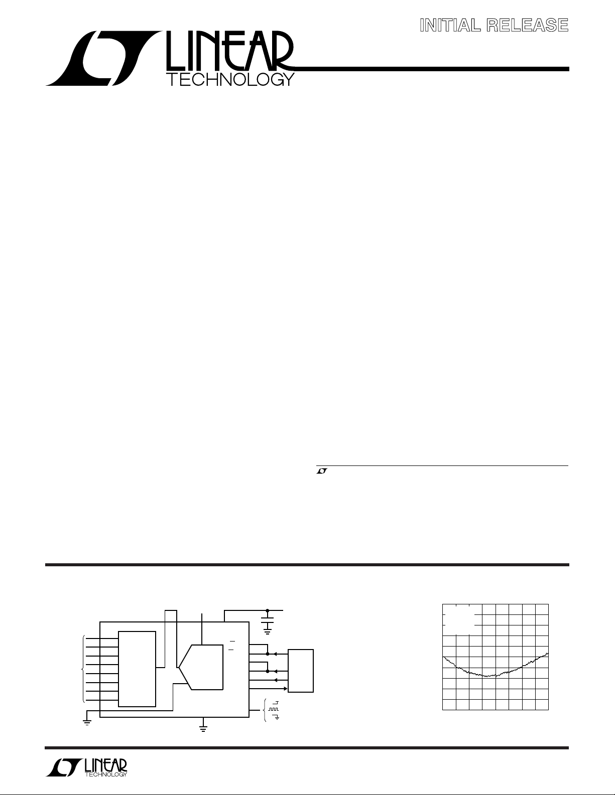
TYPICAL APPLICATIO
9
CH0
10
CH1
11
ANALOG
INPUTS
TO
–0.12V
REF
1.12V
REF
CH2
12
CH3
4-/8-CHANNEL
13
CH4*
CH5*
CH6*
CH7*
MUX
SET
14
15
17
5ZS
*THESE PINS ARE NO CONNECTS ON THE LTC2404
U
0.1V TO V
7 4 3 2, 8
ADCINMUXOUT
1, 6, 16, 18, 22, 27, 28
Information furnished by Linear Technology Corporation is believed to be accurate and reliable.
However, no responsibility is assumed for its use. Linear Technology Corporation makes no representation that the interconnection of its circuits as described herein will not infringe on existing patent rights.
CC
FS
SETVCC
20-BIT
+
∆∑ ADC
–
LTC2424/LTC2428
GND
CSADC
CSMUX
SCK
CLK
SDO
24248 TA01
23
20
25
19
21
D
IN
24
26
F
O
2.7V TO 5.5V
1µF
SERIAL DATA LINK
MICROWIRE AND
SPI COMPATABLE
MPU
V
CC
= INTERNAL OSC/50Hz REJECTION
= EXTERNAL CLOCK SOURCE
= INTERNAL OSC/60Hz REJECTION
Total Unadjusted Error vs Output Code
10
VCC = 5V
8
V
= 5V
REF
T
= 25°C
A
6
F
= LOW
O
4
2
0
–2
–4
LINEARITY ERROR (ppm)
–6
–8
–10
0 8,338,608 16,777,215
OUTPUT CODE (DECIMAL)
24248 TA02
1
LTC2424/LTC2428
WW
W
U
ABSOLUTE MAXIMUM RATINGS
(Notes 1, 2)
Supply Voltage (VCC) to GND.......................– 0.3V to 7V
Analog Input Voltage to GND ....... –0.3V to (VCC + 0.3V)
Reference Input Voltage to GND .. –0.3V to (VCC + 0.3V)
Digital Input Voltage to GND........ –0.3V to (VCC + 0.3V)
Digital Output Voltage to GND ..... –0.3V to (VCC + 0.3V)
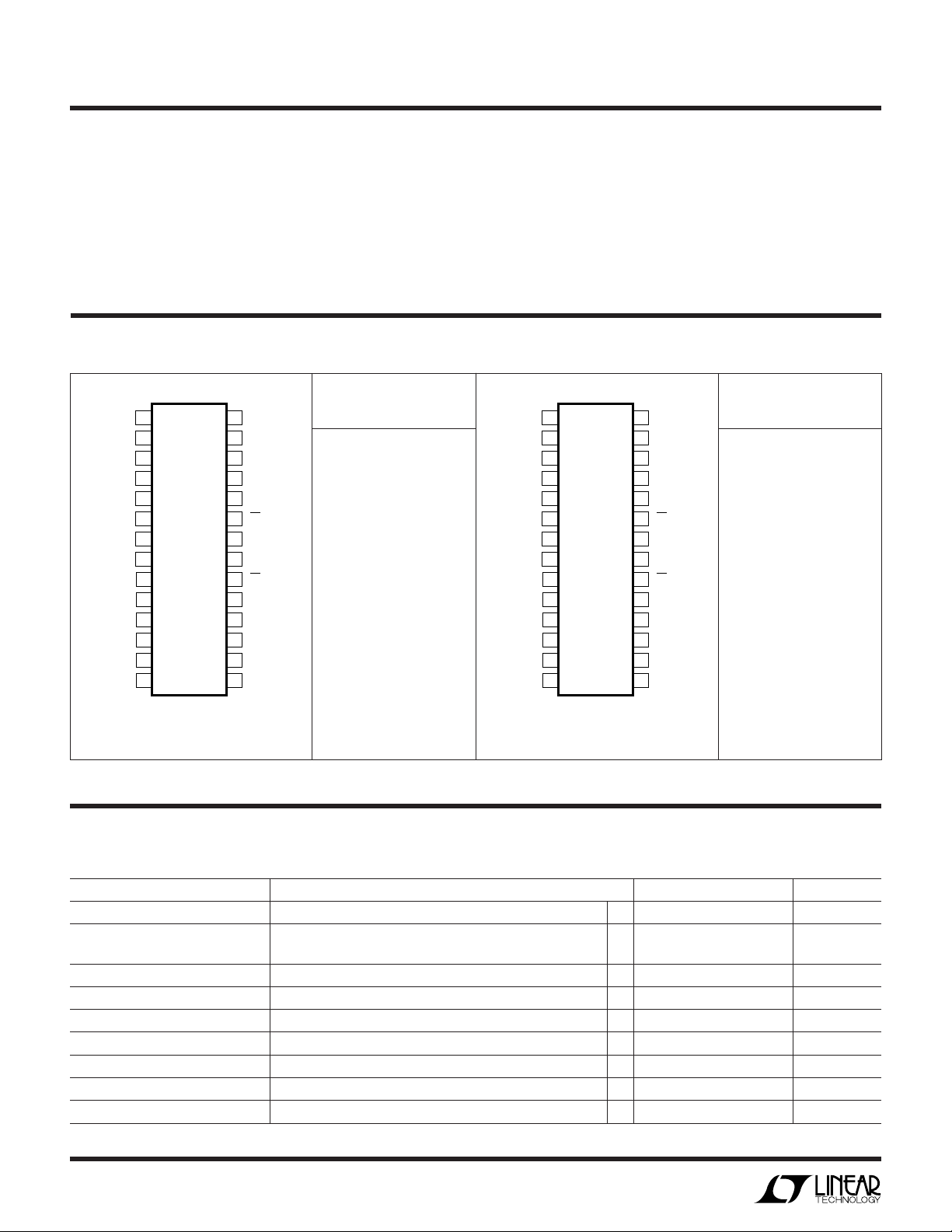
U
W
PACKAGE/ORDER INFORMATION
ORDER
PART NUMBER
LTC2424CG
LTC2424IG
GND
V
FS
SET
ADCIN
ZS
SET
GND
MUXOUT
V
CH0
CH1
CH2
CH3
NC
NC
TOP VIEW
1
2
CC
3
4
5
6
7
8
CC
9
10
11
12
13
14
28
27
26
25
24
23
22
21
20
19
18
17
16
15
GND
GND
F
O
SCK
SDO
CSADC
GND
D
IN
CSMUX
CLK
GND
NC
GND
NC
Operating Temperature Range
LTC2424C/LTC2428C ..............................0°C to 70°C
LTC2424I/LTC2428I ........................... – 40°C to 85°C
Storage Temperature Range ................. –65°C to 150°C
Lead Temperature (Soldering, 10 sec).................. 300°C
U
ORDER
PART NUMBER
LTC2428CG
LTC2428IG
GND
V
FS
SET
ADCIN
ZS
SET
GND
MUXOUT
V
CH0
CH1
CH2
CH3
CH4
CH5
TOP VIEW
1
2
CC
3
4
5
6
7
8
CC
9
10
11
12
13
14
28
27
26
25
24
23
22
21
20
19
18
17
16
15
GND
GND
F
O
SCK
SDO
CSADC
GND
D
IN
CSMUX
CLK
GND
CH7
GND
CH6
G PACKAGE
28-LEAD PLASTIC SSOP
T
= 125°C, θJA = 130°C/W
JMAX
G PACKAGE
28-LEAD PLASTIC SSOP
T
= 125°C, θJA = 130°C/W
JMAX
Consult factory for Military grade parts.
U
CONVERTER CHARACTERISTICS
temperature range, otherwise specifications are at TA = 25°C. (Notes 3, 4)
PARAMETER CONDITIONS MIN TYP MAX UNITS
Resolution (No Missing Codes) 0.1V ≤ V
Integral Nonlinearity V
REF
V
REF
Integral Nonlinearity (Fast Mode) 2.5V < V
Offset Error 2.5V ≤ V
Offset Error (Fast Mode) 2.5V < V
Offset Error Drift 2.5V ≤ V
Full-Scale Error 2.5V ≤ V
Full-Scale Error (Fast Mode) 2.5V < V
Full-Scale Error Drift 2.5V ≤ V
≤ VCC, (Note 5) ● 20 Bits
REF
= 2.5V (Note 6) ● 4 10 ppm of V
= 5V (Note 6) ● 8 20 ppm of V
< VCC, 100 Samples/Second, fO = 2.048MHz ● 40 250 ppm of V
REF
≤ V
REF
CC
< 5V, 100 Samples/Second, fO = 2.048MHz 3 ppm of V
REF
≤ V
REF
CC
≤ V
REF
CC
< 5V, 100 Samples/Second, fO = 2.048MHz 10 ppm of V
REF
≤ V
REF
CC
The ● denotes specifications which apply over the full operating
● 0.5 10 ppm of V
0.04 ppm of V
● 4 15 ppm of V
0.04 ppm of V
REF
REF
REF
REF
REF
REF
REF
/°C
REF
REF
/°C
2
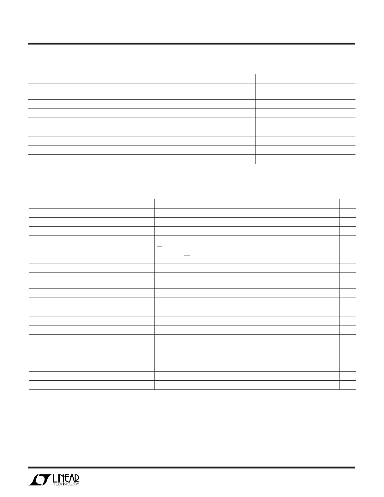
LTC2424/LTC2428
U
CONVERTER CHARACTERISTICS
temperature range, otherwise specifications are at TA = 25°C. (Notes 3, 4)
PARAMETER CONDITIONS MIN TYP MAX UNITS
Total Unadjusted Error V
Output Noise VIN = 0V, V
Output Noise (Fast Mode) V
Normal Mode Rejection 60Hz ±2% (Note 7) ● 110 130 dB
Normal Mode Rejection 50Hz ±2% (Note 8) ● 110 130 dB
Power Supply Rejection, DC V
Power Supply Rejection, 60Hz ±2% V
Power Supply Rejection, 50Hz ±2% V
= 2.5V 8 ppm of V
REF
V
= 5V 16 ppm of V
REF
= 5V (Note 13) 6 µV
REF
= 5V, 100 Samples/Second, fO = 2.048MHz 20 µV
REF
= 2.5V, VIN = 0V 100 dB
REF
= 2.5V, VIN = 0V, (Notes 7, 16) 110 dB
REF
= 2.5V, VIN = 0V, (Notes 8, 16) 110 dB
REF
The ● denotes specifications which apply over the full operating
REF
REF
RMS
RMS
UU
U
A ALOG I PUT A D REFERE CE
U
The ● denotes specifications which apply over the full operating
temperature range, otherwise specifications are at TA = 25°C. (Note 3)
SYMBOL PARAMETER CONDITIONS MIN TYP MAX UNITS
V
IN
V
REF
C
S(IN)
C
S(REF)
I
IN(LEAK)
I
REF(LEAK)
I
IN(MUX)
R
ON
I
S(OFF)
I
D(OFF)
t
OPEN
t
ON
t
OFF
QIRR MUX Off Isolation VIN = 2V
QINJ Charge Injection RS = 0Ω, CL = 1000pF, VS = 1V ±1pC
C
S(OFF)
C
D(OFF)
Input Voltage Range (Note 14) ● –0.125 • V
Reference Voltage Range ● 0.1 V
Input Sampling Capacitance 1 pF
Reference Sampling Capacitance 1.5 pF
Input Leakage Current CS = V
Reference Leakage Current V
On Channel Leakage Current VS = 2.5V (Note 15) ● ±20 nA
MUX On-Resistance I
MUX ∆RON vs Temperature 0.5 %/°C
∆RON vs VS (Note 15) 20 %
MUX Off Input Leakage Channel Off, VS = 2.5V ● ±20 nA
MUX Off Output Leakage Channel Off, VD = 2.5V ● ±20 nA
MUX Break-Before-Make Interval 290 ns
Enable Turn-On Time VS = 1.5V, RL = 3.4k, CL = 15pF 490 ns
Enable Turn-Off Time VS = 1.5V, RL = 3.4k, CL = 15pF 190 ns
Input Off Capacitance (MUX) 10 pF
Output Off Capacitance (MUX) 10 pF
CC
= 2.5V, CS = V
REF
= 1mA, VCC = 2.7V ● 250 300 Ω
OUT
I
= 1mA, VCC = 5V ● 120 250 Ω
OUT
P-P
CC
, RL = 1k, f = 100kHz 70 dB
● –100 1 100 nA
● –100 1 100 nA
REF
1.125 • V
CC
REF
V
V
3
LTC2424/LTC2428
UU
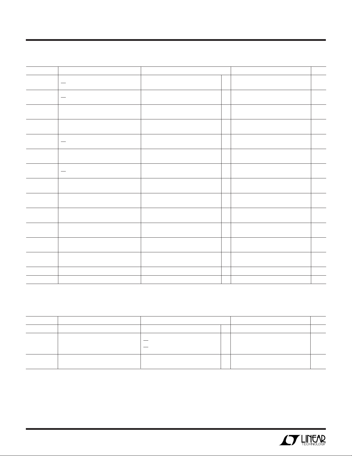
DIGITAL I PUTS A D DIGITAL OUTPUTS
operating temperature range, otherwise specifications are at TA = 25°C. (Note 3)
SYMBOL PARAMETER CONDITIONS MIN TYP MAX UNITS
V
IH
V
IL
V
IH
V
IL
I
IN
I
IN
C
IN
C
IN
V
OH
V
OL
V
OH
V
OL
I
OZ
VIN H
VIN L
MUX
MUX
High Level Input Voltage 2.7V ≤ VCC ≤ 5.5V ● 2.5 V
CS, F
O
Low Level Input Voltage 4.5V ≤ VCC ≤ 5.5V ● 0.8 V
CS, F
O
High Level Input Voltage 2.7V ≤ VCC ≤ 5.5V (Note 9) ● 2.5 V
SCK 2.7V ≤ V
Low Level Input Voltage 4.5V ≤ VCC ≤ 5.5V (Note 9) ● 0.8 V
SCK 2.7V ≤ V
Digital Input Current 0V ≤ VIN ≤ V
CS, F
O
Digital Input Current 0V ≤ VIN ≤ VCC (Note 9) ● –10 10 µA
SCK
Digital Input Capacitance 10 pF
CS, F
O
Digital Input Capacitance (Note 9) 10 pF
SCK
High Level Output Voltage IO = –800µA ● VCC – 0.5V V
SDO
Low Level Output Voltage IO = 1.6mA ● 0.4V V
SDO
High Level Output Voltage IO = –800µA (Note 10) ● VCC – 0.5V V
SCK
Low Level Output Voltage IO = 1.6mA (Note 10) ● 0.4V V
SCK
High-Z Output Leakage ● –10 10 µA
SDO
MUX High Level Input Voltage V+ = 3V ● 2V
MUX Low Level Input Voltage V+ = 2.4V ● 0.8 V
2.7V ≤ VCC ≤ 3.3V 2.0 V
2.7V ≤ VCC ≤ 5.5V 0.6 V
≤ 3.3V (Note 9) 2.0 V
CC
≤ 5.5V (Note 9) 0.6 V
CC
CC
The ● denotes specifications which apply over the full
● –10 10 µA
WU
POWER REQUIRE E TS
otherwise specifications are at TA = 25°C. (Note 3)
SYMBOL PARAMETER CONDITIONS MIN TYP MAX UNITS
V
CC
I
CC
I
CC(MUX)
Supply Voltage ● 2.7 5.5 V
Supply Current (Pin 2)
Conversion Mode CS = 0V (Note 12)
Sleep Mode CS = V
Multiplexer Supply Current (Pin 8) All Logic Inputs Tied Together ● 15 40 µA
The ● denotes specifications which apply over the full operating temperature range,
● 200 300 µA
(Note 12) ● 20 30 µA
CC
= 0V or 5V
V
IN
4
LTC2424/LTC2428
UW
TI I G CHARACTERISTICS
otherwise specifications are at TA = 25°C. (Note 3)
SYMBOL PARAMETER CONDITIONS MIN TYP MAX UNITS
f
EOSC
t
HEO
t
LEO
t
CONV
f
ISCK
D
ISCK
f
ESCK
t
LESCK
t
HESCK
t
DOUT_ISCK
t
DOUT_ESCK
t
1
t
2
t
3
t
4
t
KQMAX
t
KQMIN
t
5
t
6
External Oscillator Frequency Range 20-Bit Effective Resolution ● 2.56 307.2 kHz
External Oscillator High Period ● 0.5 390 µs
External Oscillator Low Period ● 0.5 390 µs
Conversion Time FO = 0V ● 130.66 133.33 136 ms
Internal SCK Frequency Internal Oscillator (Note 10) 19.2 kHz
Internal SCK Duty Cycle (Note 10) 45 55 %
External SCK Frequency Range (Note 9) ● 2000 kHz
External SCK Low Period (Note 9) ● 250 ns
External SCK High Period (Note 9) ● 250 ns
Internal SCK 24-Bit Data Output Time Internal Oscillator (Notes 10, 12) ● 1.23 1.25 1.28 ms
External SCK 24-Bit Data Output Time (Note 9) ● 24/f
CS ↓ to SDO Low Z ● 0 150 ns
CS ↑ to SDO High Z ● 0 150 ns
CS ↓ to SCK ↓ (Note 10) ● 0 150 ns
CS ↓ to SCK ↑ (Note 9) ● 50 ns
SCK ↓ to SDO Valid ● 200 ns
SDO Hold After SCK ↓ (Note 5) ● 15 ns
SCK Set-Up Before CS ↓ ● 50 ns
SCK Hold After CS ↓ ● 50 ns
The ● denotes specifications which apply over the full operating temperature range,
12-Bit Effective Resolution
= V
F
O
CC
External Oscillator (Note 11)
External Oscillator (Notes 10, 11) f
External Oscillator (Notes 10, 11)
● 2.56k 2.048M Hz
● 156.80 160 163.20 ms
● 20480/f
● 192/f
(in kHz) ms
EOSC
/8 kHz
EOSC
(in kHz) ms
EOSC
(in kHz) ms
ESCK
Note 1: Absolute Maximum Ratings are those values beyond which the
life of the device may be impaired.
Note 2: All voltage values are with respect to GND.
Note 3: V
is 0Ω. CSADC = CSMUX = CS. V
= 2.7 to 5.5V unless otherwise specified, source input
CC
REF
= FS
SET
– ZS
SET
.
Note 4: Internal Conversion Clock source with the FO pin tied
to GND or to V
f
= 153600Hz unless otherwise specified.
EOSC
or to external conversion clock source with
CC
Note 5: Guaranteed by design, not subject to test.
Note 6: Integral nonlinearity is defined as the deviation of a code from
a straight line passing through the actual endpoints of the transfer
curve. The deviation is measured from the center of the quantization
band.
Note 7: FO = 0V (internal oscillator) or f
= 153600Hz ±2%
EOSC
(external oscillator).
Note 8: F
= VCC (internal oscillator) or f
O
= 128000Hz ±2%
EOSC
(external oscillator).
Note 9: The converter is in external SCK mode of operation such that
the SCK pin is used as digital input. The frequency of the clock signal
driving SCK during the data output is f
and is expressed in kHz.
ESCK
Note 10: The converter is in internal SCK mode of operation such that
the SCK pin is used as digital output. In this mode of operation the
SCK pin has a total equivalent load capacitance C
Note 11: The external oscillator is connected to the F
oscillator frequency, f
, is expressed in kHz.
EOSC
= 20pF.
LOAD
pin. The external
O
Note 12: The converter uses the internal oscillator.
F
= 0V or FO = VCC.
O
Note 13: The output noise includes the contribution of the internal
calibration operations.
Note 14: For reference voltage values V
of –0.125 • V
to 1.125 • V
REF
is limited by the absolute maximum
REF
rating of the Analog Input Voltage pin (Pin 3). For 2.5V < V
0.267V + 0.89 • V
For 0.267V + 0.89 • V
+ 0.3V.
to V
CC
the input voltage range is –0.3V to 1.125 • V
CC
< V
CC
≤ VCC the input voltage range is –0.3V
REF
> 2.5V the extended input
REF
REF
≤
REF
Note 15: VS is the voltage applied to a channel input. VD is the voltage
applied to the MUX output.
Note 16: V
CC(DC)
= 4.1V, V
CC(AC)
= 2.8V
P-P
.
.
5

LTC2424/LTC2428
U
UU
PIN FUNCTIONS
GND (Pins 1, 6, 16, 18, 22, 27, 28): Ground. Should be
connected directly to a ground plane through a minimum
length trace or it should be the single-point-ground in a
single-point grounding system.
VCC (Pins 2, 8): Positive Supply Voltage. 2.7V ≤ VCC ≤
5.5V. Bypass to GND with a 10µF tantalum capacitor in
parallel with 0.1µF ceramic capacitor as close to the part
as possible.
FS
(Pin 3): Full-Scale Set Input. This pin defines the
SET
full-scale input value. When VIN = FS
full scale (FFFFFH). The total reference voltage (V
FS
– ZS
SET
ADCIN (Pin 4): Analog Input. The input voltage range is
–0.125 • V
voltage range may be limited by the pin absolute maximum rating of –0.3V to VCC + 0.3V.
ZS
(Pin 5): Zero-Scale Set Input. This pin defines the
SET
zero-scale input value. When VIN = ZS
zero scale (00000H). For pin compatibility with the LTC2404/
LTC2408 this pin must be grounded.
MUXOUT (Pin 7): MUX Output. This pin is the output of the
multiplexer. Tie to ADCIN for normal operation.
.
SET
to 1.125 • V
REF
REF
. For V
, the ADC outputs
SET
> 2.5V the input
REF
, the ADC outputs
SET
REF
) is
CSMUX (Pin 20): MUX Chip Select Input. A logic high on
this input allows the MUX to receive a channel address. A
logic low enables the selected MUX channel and connects
it to the MUXOUT pin for A/D conversion. For normal
operation, drive this pin in parallel with CSADC.
DIN (Pin 21): Digital Data Input. The multiplexer address
is shifted into this input on the last four rising CLK edges
before CSMUX goes low.
CSADC (Pin 23): ADC Chip Select Input. A low on this pin
enables the SDO digital output and following each conversion, the ADC automatically enters the Sleep mode and
remains in this low power state as long as CSADC is high.
A high on this pin also disables the SDO digital output. A
low-to-high transition on CSADC during the Data Output
state aborts the data transfer and starts a new conversion.
For normal operation, drive this pin in parallel with CSMUX.
SDO (Pin 24): Three-State Digital Output. During the data
output period this pin is used for serial data output. When
the chip select CSADC is high (CSADC = VCC), the SDO pin
is in a high impedance state. During the Conversion and
Sleep periods, this pin can be used as a conversion status
output. The conversion status can be observed by pulling
CSADC low.
CH0 (Pin 9): Analog Multiplexer Input.
CH1 (Pin 10): Analog Multiplexer Input.
CH2 (Pin 11): Analog Multiplexer Input.
CH3 (Pin 12): Analog Multiplexer Input.
CH4 (Pin 13): Analog Multiplexer Input. No connect on the
LTC2424.
CH5 (Pin 14): Analog Multiplexer Input. No connect on the
LTC2424.
CH6 (Pin 15): Analog Multiplexer Input. No connect on the
LTC2424.
CH7 (Pin 17): Analog Multiplexer Input. No connect on the
LTC2424.
CLK (Pin 19): Shift Clock for Data In. This clock synchro-
nizes the serial data transfer into the MUX. For normal
operation, drive this pin in parallel with SCK.
SCK (Pin 25): Shift Clock for Data Out. This clock synchronizes the serial data transfer of the ADC data output. Data
is shifted out of SDO on the falling edge of SCK. For normal
operation, drive this pin in parallel with CLK.
FO (Pin 26): Digital input which controls the ADC’s notch
frequencies and conversion time. When the FO pin is
connected to VCC (FO = VCC), the converter uses its internal
oscillator and the digital filter first null is located at 50Hz.
When the FO pin is connected to GND (FO = OV), the
converter uses its internal oscillator and the digital filter
first null is located at 60Hz. When FO is driven by an
external clock signal with a frequency f
uses this signal as its clock and the digital filter first null is
located at a frequency f
word rate is f
EOSC
/20480.
/2560. The resulting output
EOSC
, the converter
EOSC
6
LTC2424/LTC2428
3.4k
SDO
24248 TC02
Hi-Z TO V
OL
VOH TO V
OL
VOL TO Hi-Z
C
LOAD
= 20pF
V
CC
UU
W
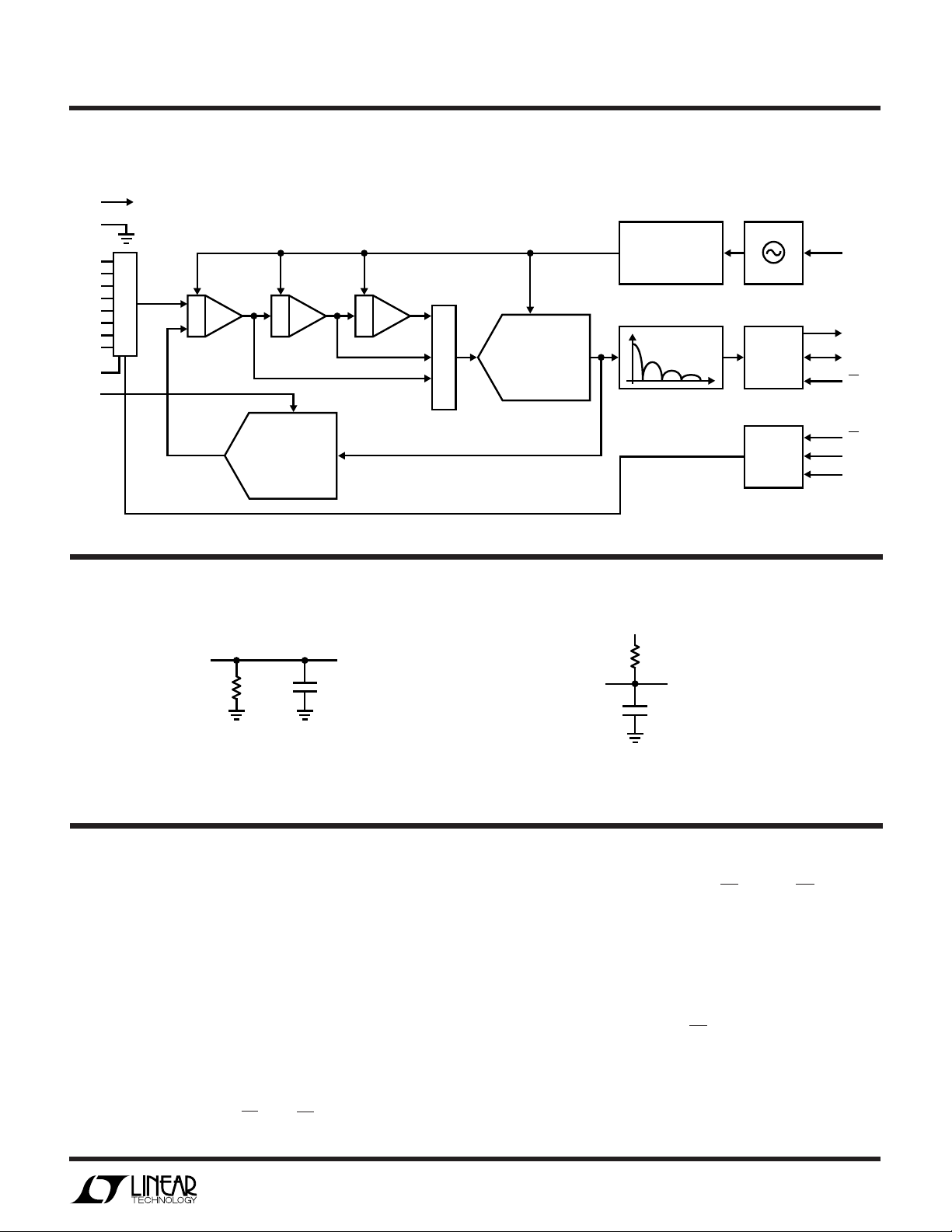
FU CTIO AL BLOCK DIAGRA
V
CC
GND
CH0
CH1
CH2
CH3
CH4
CH5
CH6
CH7
ZS
FS
SET
8-CHANNEL MUX
SET
DAC
∫∫∫
∑
ADC
AUTOCALIBRATION
AND CONTROL
DECIMATING FIR
INTERNAL
OSCILLATOR
SERIAL
INTERFACE
CHANNEL
SELECT
(INT/EXT)
24248 BD
F
O
SDO
SCK
CSADC
CSMUX
D
IN
CLK
TEST CIRCUITS
SDO
3.4k
Hi-Z TO V
VOL TO V
VOH TO Hi-Z
U
OH
OH
= 20pF
C
LOAD
24248 TC01
WUU
APPLICATIONS INFORMATION
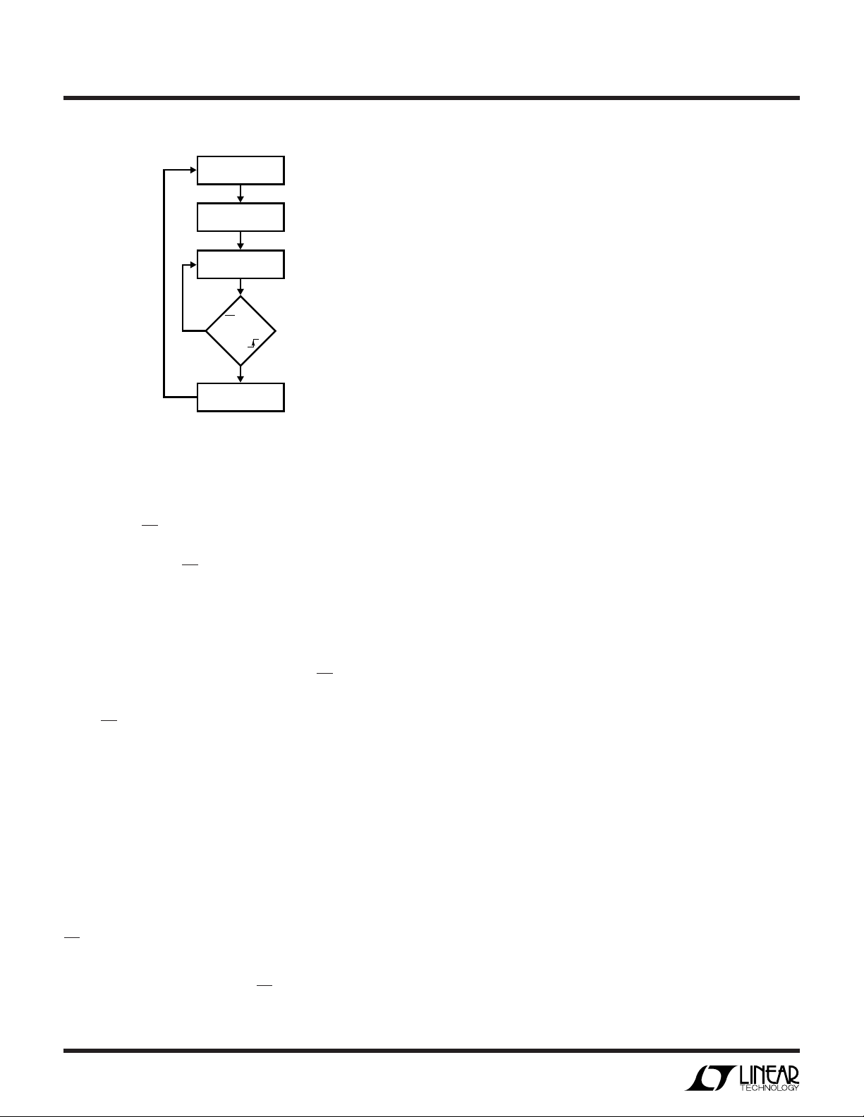
Converter Operation Cycle
The LTC2424/LTC2428 are low power, 4-/8-channel deltasigma analog-to-digital converters with easy-to-use
4-wire interfaces. Their operation is simple and made up
of four states. The converter operation begins with the
conversion, followed by a low power sleep state and
concluded with the data output (see Figure 1). Channel
selection may be performed while the device is in the sleep
state or at the conclusion of the data output state. The
interface consists of serial data output (SDO), serial clock
(CLK/SCK), chip select (CSADC/CSMUX) and data input
(DIN). By tying SCK to CLK and CSADC to CSMUX, the
interface requires only four wires.
Initially, the LTC2424 or LTC2428 performs a conversion.
Once the conversion is complete, the device enters the
sleep state. While in the sleep state, power consumption
is reduced by an order of magnitude. The part remains in
the sleep state as long as CSADC is logic HIGH. The
conversion result is held indefinitely in a static shift
register while the converter is in the sleep state.
Channel selection for the next conversion cycle is performed while the device is in the sleep state or at the end
7
LTC2424/LTC2428
U
WUU
APPLICATIONS INFORMATION
CONVERT
CHANNEL SELECT
(SLEEP)
SLEEP
CSADC
1
AND
SCK
0
DATA OUTPUT
(CHANNEL SELECT)
Figure 1. LTC2428 State Transition Diagram
of the data output state. A specific channel is selected by
applying a 4-bit serial word to the DIN pin on the rising edge
of CLK while CSMUX is HIGH, see Figure 4 and Table 3. The
channel is selected based on the last four bits clocked into
the DIN pin before CSMUX goes low. If DIN is all 0’s, the
previous channel remains selected.
In the example, Figure 4, the MUX channel is selected
during the sleep state, just before the data output state
begins. Once the channel selection is complete, the device
remains in the sleep state as long as CSADC remains
HIGH.
Once CSADC is pulled low, the device begins outputting
the conversion result. There is no latency in the conversion
result. Since there is no latency, the first conversion
following a change in input channel is valid and corresponds to that channel. The data output corresponds to
the conversion just performed. This result is shifted out on
the serial data output pin (SDO) under the control of the
serial clock (SCK). Data is updated on the falling edge of
SCK allowing the user to reliably latch data on the rising
edge of SCK, see Figure 4. The data output state is
concluded once 24 bits are read out of the ADC or when
CSADC is brought HIGH. The device automatically initiates
a new conversion and the cycle repeats.
Through timing control of the CSADC and SCK pins, the
LTC2424/LTC2428 offer two modes of operation: internal
24248 F01
or external SCK. These modes do not require programming configuration registers; moreover, they do not disturb the cyclic operation described above. These modes of
operation are described in detail in the Serial Interface
Timing Modes section.
Conversion Clock
A major advantage delta-sigma converters offer over
conventional type converters is an on-chip digital filter
(commonly known as Sinc or Comb filter). For high
resolution, low frequency applications, this filter is typically designed to reject line frequencies of 50 or 60Hz plus
their harmonics. In order to reject these frequencies in
excess of 110dB, a highly accurate conversion clock is
required. The LTC2424/LTC2428 incorporate an on-chip
highly accurate oscillator. This eliminates the need for
external frequency setting components such as crystals or
oscillators. Clocked by the on-chip oscillator, the LTC2424/
LTC2428 reject line frequencies (50 or 60Hz ±2%) a
minimum of 110dB.
Ease of Use
The LTC2424/LTC2428 data output has no latency, filter
settling or redundant data associated with the conversion
cycle. There is a one-to-one correspondence between the
conversion and the output data. Therefore, multiplexing
an analog input voltage is easy.
The LTC2424/LTC2428 perform offset and full-scale calibrations every conversion cycle. This calibration is transparent to the user and has no effect on the cyclic operation
described above. The advantage of continuous calibration
is extreme stability of offset and full-scale readings with
respect to time, supply voltage change and temperature
drift.
Power-Up Sequence
The LTC2424/LTC2428 automatically enter an internal
reset state when the power supply voltage VCC drops
below approximately 2.2V. When the VCC voltage rises
above this critical threshold, the converter creates an
internal power-on-reset (POR) signal with duration of
approximately 0.5ms. The POR signal clears all internal
registers within the ADC and initiates a conversion. At
8
LTC2424/LTC2428
U
WUU
APPLICATIONS INFORMATION
power-up, the multiplexer channel is disabled and should
be programmed once the device enters the sleep state.
The results of the first conversion following a POR are not
valid since a multiplexer channel was disabled.
Reference Voltage Range
The LTC2424/LTC2428 can accept a reference voltage
from 0V to VCC. The converter output noise is determined
by the thermal noise of the front-end circuits, and as such,
its value in microvolts is nearly constant with reference
voltage. A decrease in reference voltage will not significantly improve the converter’s effective resolution. On the
other hand, a reduced reference voltage will improve the
overall converter INL performance. The recommended
range for the LTC2424/LTC2428 voltage reference is
100mV to VCC.
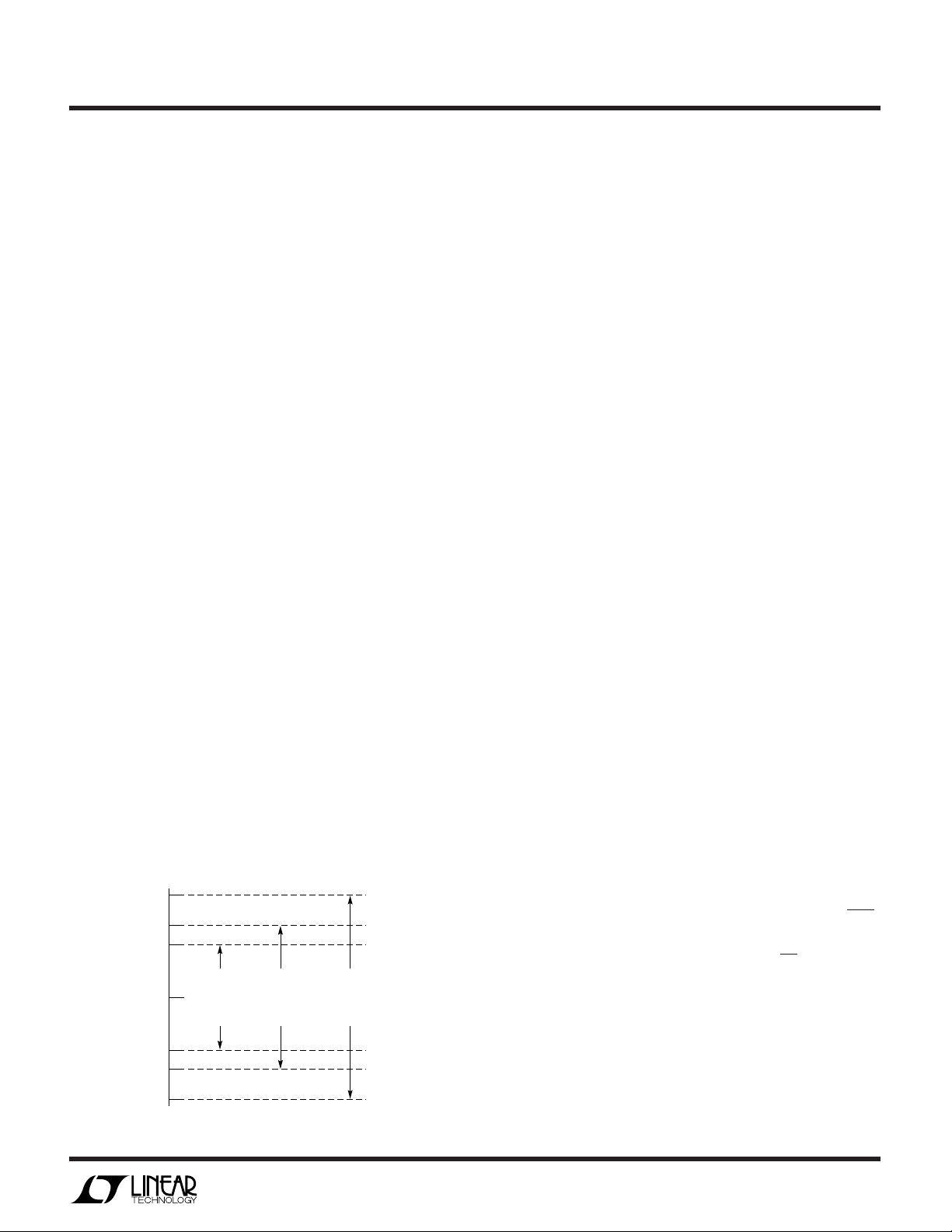
Input Voltage Range
The converter is able to accommodate system level offset
and gain errors as well as system level overrange
situations due to its extended input range, see Figure 2.
The LTC2424/LTC2428 converts input signals within the
extended input range of –0.125 • V
(V
= FS
REF
For large values of V
SET
– ZS
).
SET
this range is limited to a voltage
REF
range of – 0.3V to (VCC + 0.3V). Beyond this range the input
ESD protection devices begin to turn on and the errors due
to the input leakage current increase rapidly.
Input signals applied to VIN may extend below ground by
– 300mV and above VCC by 300mV. In order to limit any fault
current, a resistor of up to 5k may be added in series with
VCC + 0.3V
to 1.125 • V
REF
REF
any channel input pin (CH0 to CH7) without affecting the
performance of the device. In the physical layout, it is important to maintain the parasitic capacitance of the connection between this series resistance and the channel input
pin as low as possible; therefore, the resistor should be
located as close as practical to the channel input pin. The
effect of the series resistance on the converter accuracy can
be evaluated from the curves presented in the Analog Input/Reference Current section. In addition, a series resistor will introduce a temperature dependent offset error due
to the input leakage current. A 1nA input leakage current
will develop a 1ppm offset error on a 5k resistor if V
REF
=
5V. This error has a very strong temperature dependency.
Output Data Format
The LTC2424/LTC2428 serial output data stream is 24 bits
long. The first 4 bits represent status information indicating the sign, input range and conversion state. The next 20
bits are the conversion result, MSB first.
The LTC2424/LTC2428 can be interchanged with the
LTC2404/LTC2408. The two devices are designed to allow
the user to incorporate either device in the same design as
long as ZS
of the LTC2424/LTC2428 is tied to ground.
SET
While the LTC2424/LTC2428 output word lengths are 24
bits (as opposed to the 32-bit output of the LTC2404/
LTC2408), their output clock timing can be identical to the
LTC2404/LTC2408. As shown in Figure 3, the LTC2424/
LTC2408 data output is concluded on the falling edge of the
24th serial clock (SCK). In order to maintain drop-in compatibility with the LTC2404/LTC2408, it is possible to clock
the LTC2424/LTC2428 with an additional 8 serial clock
pulses. This results in 8 additional output bits which are
always logic HIGH.
9/8V
REF
V
REF
NORMAL
1/2V
REF
0
–1/8V
REF
–0.3V
Figure 2. LTC2424/LTC2428 Input Range
INPUT
RANGE
EXTENDED
INPUT
RANGE
ABSOLUTE
MAXIMUM
INPUT
RANGE
24248 F02
Bit 23 (first output bit) is the end of conversion (EOC)
indicator. This bit is available at the SDO pin during the
conversion and sleep states whenever the CS pin is LOW.
This bit is HIGH during the conversion and goes LOW
when the conversion is complete.
Bit 22 (second output bit) is a dummy bit (DMY) and is
always LOW.
Bit 21 (third output bit) is the conversion result sign indicator (SIG). If VIN is >0, this bit is HIGH. If VIN is <0, this
bit is LOW. The sign bit changes state during the zero code.
9
 Loading...