

Linear Technology LTC2420 Datasheet
No Latency ∆Σ
Final Electrical Specifications
LTC2420
20-Bit µPower
TM
ADC in SO-8
FEATURES
■
20-Bit ADC in SO-8 Package
■
8ppm INL, No Missing Codes at 20 Bits
■
4ppm Full-Scale Error
■
0.5ppm Offset
■
1.2ppm Noise
■
Digital Filter Settles in a Single Cycle. Each
Conversion Is Accurate, Even After an Input Step.
■
Internal Oscillator—No External Components
Required
■
Fast Mode: 16-Bit Noise, 12 Bits TUE at 100sps
■
110dB Min, 50Hz/60Hz Notch Filter
■
Reference Input Voltage: 0.1V to V
■
Live Zero—Extended Input Range Accommodates
CC
12.5% Overrange and Underrange
■
Single Supply 2.7V to 5.5V Operation
■
Low Supply Current (200µA) and Auto Shutdown
■
Pin Compatible with 24-Bit LTC2400
U
APPLICATIO S
■
Weight Scales
■
Direct Temperature Measurement
■
Gas Analyzers
■
Strain-Gage Transducers
■
Instrumentation
■
Data Acquisition
■
Industrial Process Control
■
4-Digit DVMs
U
January 2000
DESCRIPTIO
The LTC®2420 is a micropower 20-bit A/D converter with
an integrated oscillator, 8ppm INL and 1.2ppm RMS
noise that operates from 2.7V to 5.5V. It uses delta-sigma
technology and provides a digital filter that settles in a
single cycle for multiplexed applications. Through a single
pin, the LTC2420 can be configured for better than 110dB
rejection at 50Hz or 60Hz ±2%, or it can be driven by an
external oscillator for a user-defined rejection frequency
in the range 1Hz to 800Hz. The internal oscillator requires
no external frequency setting components.
The converter accepts any external reference voltage from
0.1V to VCC. With its extended input conversion range of
–12.5% V
resolves the offset and overrange problems of preceding
sensors or signal conditioning circuits.
The LTC2420 communicates through a flexible 3-wire
digital interface which is compatible with SPI and
MICROWIRETM protocols.
, LTC and LT are registered trademarks of Linear Technology Corporation.
No Latency ∆Σ is a trademark of Linear Technology Corporation.
MICROWIRE is a trademark of National Semiconductor Corporation.
to 112.5% V
REF
, the LTC2420 smoothly
REF
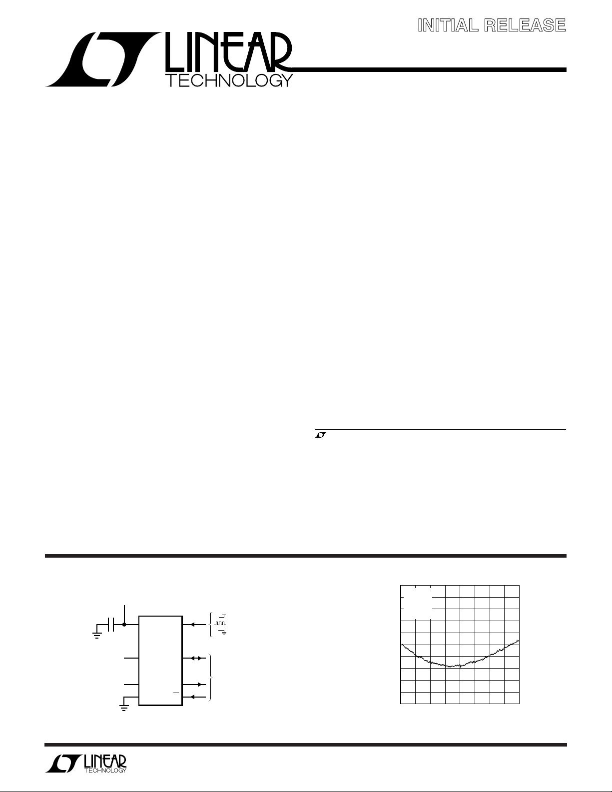
TYPICAL APPLICATIO
2.7V TO 5.5V
1µF
1
REFERENCE
VOLTAGE
0.1V TO V
ANALOG
INPUT RANGE
TO 1.12V
–0.12V
REF
REF
2
CC
3
4
V
CC
LTC2420
V
SCK
REF
SDO
V
IN
GND CS
U
Total Unadjusted Error vs Output Code
10
VCC = 5V
8
= 5V
V
REF
= 25°C
T
V
CC
8
F
O
7
6
5
Information furnished by Linear Technology Corporation is believed to be accurate and reliable.
However, no responsibility is assumed for its use. Linear Technology Corporation makes no representation that the interconnection of its circuits as described herein will not infringe on existing patent rights.
= INTERNAL OSC/50Hz REJECTION
= EXTERNAL CLOCK SOURCE
= INTERNAL OSC/60Hz REJECTION
3-WIRE
SPI INTERFACE
2420 TA01
A
6
= LOW
F
O
4
2
0
–2
–4
–6
TOTAL UNADJUSTED ERROR (ppm)
–8
–10
0 524,288 1,048,575
OUTPUT CODE (DECIMAL)
2420 TA02
1
LTC2420
WW
W
ABSOLUTE MAXIMUM RATINGS
U
UUW
PACKAGE/ORDER INFORMATION
(Notes 1, 2)
Supply Voltage (VCC) to GND.......................– 0.3V to 7V
Analog Input Voltage to GND ....... –0.3V to (VCC + 0.3V)
Reference Input Voltage to GND .. –0.3V to (VCC + 0.3V)
Digital Input Voltage to GND........ –0.3V to (VCC + 0.3V)
Digital Output Voltage to GND ..... –0.3V to (VCC + 0.3V)
Operating Temperature Range
LTC2420C ............................................... 0°C to 70°C
LTC2420I............................................ –40°C to 85°C
Storage Temperature Range ................. –65°C to 150°C
TOP VIEW
V
1
CC
V
2
REF
V
3
IN
GND
4
S8 PACKAGE
8-LEAD PLASTIC SO
T
= 125°C, θJA = 130°C/W
JMAX
Consult factory for Military grade parts.
8
F
O
SCK
7
SDO
6
CS
5
ORDER PART NUMBER
LTC2420CS8
LTC2420IS8
S8 PART MARKING
2420
2420I
Lead Temperature (Soldering, 10 sec)..................300°C
U
CONVERTER CHARACTERISTICS
temperature range, otherwise specifications are at TA = 25°C. (Notes 3, 4)
PARAMETER CONDITIONS MIN TYP MAX UNITS
Resolution (No Missing Codes) 0.1V ≤ V
Integral Nonlinearity V
Integral Nonlinearity (Fast Mode) V
Offset Error 2.5V ≤ V
Offset Error (Fast Mode) 2.5V < V
Offset Error Drift 2.5V ≤ V
Full-Scale Error 2.5V ≤ V
Full-Scale Error (Fast Mode) 2.5V < V
Full-Scale Error Drift 2.5V ≤ V
Total Unadjusted Error V
Output Noise VIN = 0V (Note 13) 6 µV
Output Noise (Fast Mode) V
Normal Mode Rejection 60Hz ±2% (Note 7) ● 110 130 dB
Normal Mode Rejection 50Hz ±2% (Note 8) ● 110 130 dB
Power Supply Rejection, DC V
Power Supply Rejection, 60Hz ±2% V
Power Supply Rejection, 50Hz ±2% V
REF
V
REF
REF
REF
V
REF
REF
REF
REF
REF
≤ VCC, (Note 5) ● 20 Bits
REF
= 2.5V (Note 6) ● 4 10 ppm of V
= 5V (Note 6) ● 8 20 ppm of V
= 5V, V
= 2.5V 8 ppm of V
= 5V 16 ppm of V
= 5V, 100 Samples/Second, fO = 2.048MHz 20 µV
= 2.5V, VIN = 0V 100 dB
= 2.5V, VIN = 0V, (Note 7) 110 dB
= 2.5V, VIN = 0V, (Note 8) 110 dB
= 2.5V, 100 Samples/Second, fO = 2.048MHz ● 40 250 ppm of V
REF
≤ V
REF
CC
< 5V, 100 Samples/Second, fO = 2.048MHz 3 ppm of V
REF
≤ V
REF
CC
≤ V
REF
CC
< 5V, 100 Samples/Second, fO = 2.048MHz 10 ppm of V
REF
≤ V
REF
CC
The ● denotes specifications which apply over the full operating
● 0.5 10 ppm of V
0.04 ppm of V
● 4 10 ppm of V
0.04 ppm of V
REF
REF
REF
REF
REF
REF
REF
/°C
REF
REF
/°C
REF
REF
RMS
RMS
2
LTC2420
UU
U
A ALOG I PUT A D REFERE CE
U
The ● denotes specifications which apply over the full operating
temperature range, otherwise specifications are at TA = 25°C. (Note 3)
SYMBOL PARAMETER CONDITIONS MIN TYP MAX UNITS
V
IN
V
REF
C
S(IN)
C
S(REF)
I
IN(LEAK)
I
REF(LEAK)
Input Voltage Range (Note 14) ● –0.125 • V
Reference Voltage Range ● 0.1 V
Input Sampling Capacitance 1 pF
Reference Sampling Capacitance 1.5 pF
Input Leakage Current CS = V
Reference Leakage Current V
= 2.5V, CS = V
REF
CC
CC
● –100 1 100 nA
● –100 1 100 nA
REF
1.125 • V
CC
REF
UU
DIGITAL I PUTS A D DIGITAL OUTPUTS
operating temperature range, otherwise specifications are at TA = 25°C. (Note 3)
SYMBOL PARAMETER CONDITIONS MIN TYP MAX UNITS
V
IH
V
IL
V
IH
V
IL
I
IN
I
IN
C
IN
C
IN
V
OH
V
OL
V
OH
V
OL
I
OZ
High Level Input Voltage 2.7V ≤ VCC ≤ 5.5V ● 2.5 V
CS, F
O
Low Level Input Voltage 4.5V ≤ VCC ≤ 5.5V ● 0.8 V
CS, F
O
High Level Input Voltage 2.7V ≤ VCC ≤ 5.5V (Note 9) ● 2.5 V
SCK 2.7V ≤ V
Low Level Input Voltage 4.5V ≤ VCC ≤ 5.5V (Note 9) ● 0.8 V
SCK 2.7V ≤ V
Digital Input Current 0V ≤ VIN ≤ V
CS, F
O
Digital Input Current 0V ≤ VIN ≤ VCC (Note 9) ● –10 10 µA
SCK
Digital Input Capacitance 10 pF
CS, F
O
Digital Input Capacitance (Note 9) 10 pF
SCK
High Level Output Voltage IO = –800µA ● VCC – 0.5 V
SDO
Low Level Output Voltage IO = 1.6mA ● 0.4 V
SDO
High Level Output Voltage IO = –800µA (Note 10) ● VCC – 0.5 V
SCK
Low Level Output Voltage IO = 1.6mA (Note 10) ● 0.4 V
SCK
High-Z Output Leakage ● –10 10 µA
SDO
2.7V ≤ VCC ≤ 3.3V 2.0 V
2.7V ≤ VCC ≤ 5.5V 0.6 V
The ● denotes specifications which apply over the full
≤ 3.3V (Note 9) 2.0 V
CC
≤ 5.5V (Note 9) 0.6 V
CC
CC
● –10 10 µA
V
V
WU
POWER REQUIRE E TS
The ● denotes specifications which apply over the full operating temperature range,
otherwise specifications are at TA = 25°C. (Note 3)
SYMBOL PARAMETER CONDITIONS MIN TYP MAX UNITS
V
CC
I
CC
Supply Voltage ● 2.7 5.5 V
Supply Current
Conversion Mode CS = 0V (Note 12)
Sleep Mode CS = V
(Note 12) ● 20 30 µA
CC
● 200 300 µA
3
LTC2420
UW
TI I G CHARACTERISTICS
range, otherwise specifications are at TA = 25°C. (Note 3)
SYMBOL PARAMETER CONDITIONS MIN TYP MAX UNITS
f
EOSC
t
HEO
t
LEO
t
CONV
f
ISCK
D
ISCK
f
ESCK
t
LESCK
t
HESCK
t
DOUT_ISCK
t
DOUT_ESCK
t
1
t2 CS ↑ to SDO High Z ● 0 150 ns
t3 CS ↓ to SCK ↓ (Note 10) ● 0 150 ns
t4 CS ↓ to SCK ↑ (Note 9) ● 50 ns
t
KQMAX
t
KQMIN
t
5
t
6
External Oscillator Frequency Range 20-Bit Effective Resolution ● 2.56 307.2 kHz
External Oscillator High Period ● 0.5 390 µs
External Oscillator Low Period ● 0.5 390 µs
Conversion Time FO = 0V ● 130.66 133.33 136 ms
Internal SCK Frequency Internal Oscillator (Note 10) 19.2 kHz
Internal SCK Duty Cycle (Note 10) 45 55 %
External SCK Frequency Range (Note 9) ● 2000 kHz
External SCK Low Period (Note 9) ● 250 ns
External SCK High Period (Note 9) ● 250 ns
Internal SCK 24-Bit Data Output Time Internal Oscillator (Notes 10, 12) ● 1.23 1.25 1.28 ms
External SCK 24-Bit Data Output Time (Note 9) ● 24/f
CS ↓ to SDO Low Z ● 0 150 ns
SCK ↓ to SDO Valid ● 200 ns
SDO Hold After SCK ↓ (Note 5) ● 15 ns
SCK Set-Up Before CS ↓ ● 50 ns
SCK Hold After CS ↓ ● 50 ns
The ● denotes specifications which apply over the full operating temperature
12-Bit Effective Resolution
= V
F
O
CC
External Oscillator (Note 11)
External Oscillator (Notes 10, 11) f
External Oscillator (Notes 10, 11)
● 2.56 2.048 MHz
● 156.80 160 163.20 ms
● 20480/f
● 192/f
(in kHz) ms
EOSC
/8 kHz
EOSC
(in kHz) ms
EOSC
(in kHz) ms
ESCK
Note 1: Absolute Maximum Ratings are those values beyond which the
life of the device may be impaired.
Note 2: All voltage values are with respect to GND.
Note 3: All voltages are with respect to GND. V
otherwise specified. R
SOURCE
= 0Ω.
= 2.7 to 5.5V unless
CC
Note 4: Internal Conversion Clock source with the FO pin tied
to GND or to V
= 153600Hz unless otherwise specified.
f
EOSC
or to external conversion clock source with
CC
Note 5: Guaranteed by design, not subject to test.
Note 6: Integral nonlinearity is defined as the deviation of a code from
a straight line passing through the actual endpoints of the transfer
curve. The deviation is measured from the center of the quantization
band.
Note 7: FO = 0V (internal oscillator) or f
= 153600Hz ±2%
EOSC
(external oscillator).
Note 8: F
= VCC (internal oscillator) or f
O
= 128000Hz ±2%
EOSC
(external oscillator).
Note 9: The converter is in external SCK mode of operation such that
the SCK pin is used as digital input. The frequency of the clock signal
driving SCK during the data output is f
and is expressed in kHz.
ESCK
Note 10: The converter is in internal SCK mode of operation such that
the SCK pin is used as digital output. In this mode of operation the
SCK pin has a total equivalent load capacitance C
LOAD
= 20pF.
Note 11: The external oscillator is connected to the FO pin. The external
oscillator frequency, f
, is expressed in kHz.
EOSC
Note 12: The converter uses the internal oscillator.
= 0V or FO = VCC.
F
O
Note 13: The output noise includes the contribution of the internal
calibration operations.
Note 14: For reference voltage values V
of –0.125 • V
to 1.125 • V
REF
is limited by the absolute maximum
REF
rating of the Analog Input Voltage pin (Pin 3). For 2.5V < V
0.267V + 0.89 • V
For 0.267V + 0.89 • V
to V
+ 0.3V.
CC
the input voltage range is –0.3V to 1.125 • V
CC
< V
CC
≤ VCC the input voltage range is –0.3V
REF
> 2.5V the extended input
REF
REF
≤
.
REF
4
 Loading...