

FEATURES
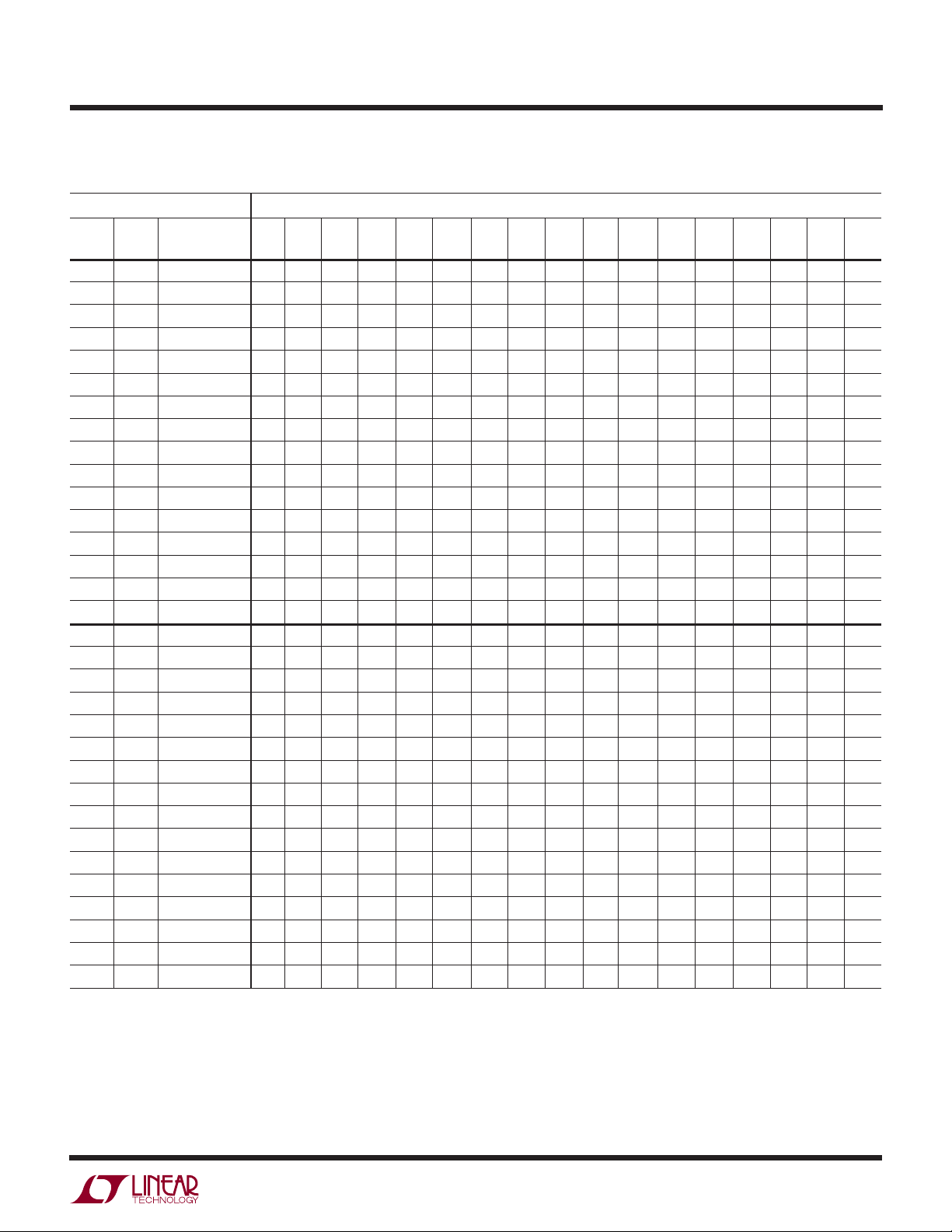
INPUT VOLTAGE (V)
–2.5 –2 –1 0 1.0 2.0
TUE (ppm OF V
REF
)
3
2
1
0
–1
–2
–3
–1.5 –0.5 0.5 1.5
2414/18 TA01b
2.5
VCC = 5V
V
REF
= 5V
V
INCM
= V
REFCM
= 2.5V
F
O
= GND
TA = 85°C
TA = 25°C
TA = –45°C
LTC2414/LTC2418
8-/16-Channel
24-Bit No Latency ∆Σ
U
DESCRIPTIO
TM
ADCs
■
8-/16-Channel Single-Ended or 4-/8-Channel
Differential Inputs (LTC2414/LTC2418)
■
Low Supply Current (200µA, 4µA in Autosleep)
■
Differential Input and Differential Reference
with GND to V
■
2ppm INL, No Missing Codes
■
2.5ppm Full-Scale Error and 0.5ppm Offset
■
0.2ppm Noise
■
No Latency: Digital Filter Settles in a Single Cycle
Common Mode Range
CC
Each Conversion Is Accurate, Even After a New
Channel is Selected
■
Single Supply 2.7V to 5.5V Operation
■
Internal Oscillator—No External Components
Required
■
110dB Min, 50Hz/60Hz Notch Filter
U
APPLICATIO S
■
Direct Sensor Digitizer
■
Weight Scales
■
Direct Temperature Measurement
■
Gas Analyzers
■
Strain Gauge Transducers
■
Instrumentation
■
Data Acquisition
■
Industrial Process Control
The LTC®2414/LTC2418 are 8-/16-channel (4-/8-differential) micropower 24-bit ∆Σ analog-to-digital converters. They operate from 2.7V to 5.5V and include an
integrated oscillator, 2ppm INL and 0.2ppm RMS noise.
They use delta-sigma technology and provide single cycle
settling time for multiplexed applications. Through a
single pin, the
LTC2414/LTC2418
can be configured for
better than 110dB differential mode rejection at 50Hz or
60Hz ± 2%, or they can be driven by an external oscillator
for a user-defined rejection frequency. The internal oscillator requires no external frequency setting components.
The LTC2414/LTC2418 accept any external differential
reference voltage from 0.1V to V
for flexible ratiometric
CC
and remote sensing measurement applications. They can
be configured to take 4/8 differential channels or
8/16 single-ended channels. The full-scale bipolar input
range is from – 0.5V
mode voltage, V
age, V
INCM
REFCM
, may be independently set within GND to VCC.
to 0.5V
REF
, and the input common mode volt-
. The reference common
REF
The DC common mode input rejection is better than 140dB.
The LTC2414/LTC2418 communicate through a flexible
4-wire digital interface that is compatible with SPI and
TM
MICROWIRE
, LTC and LT are registered trademarks of Linear Technology Corporation.
No Latency ∆Σ is a trademark of Linear Technology Corporation. All other trademarks are the
property of their respective owners.
protocols.
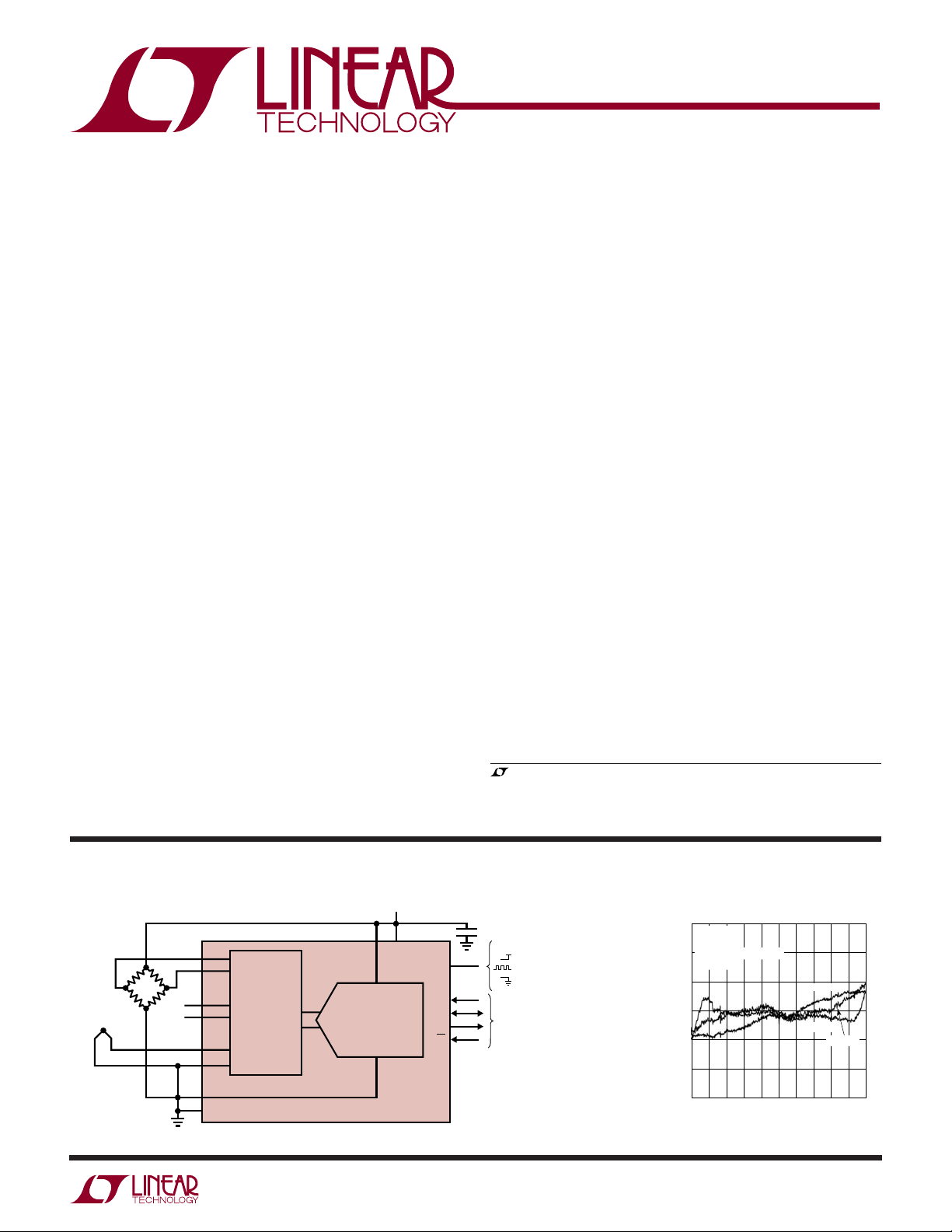
TYPICAL APPLICATIO
THERMOCOUPLE
21
22
8
10
12
15
CH0
CH1
CH7
CH8281
CH15
COM
REF
GND
•
•
•
•
•
•
–
16-CHANNEL
MUX
U
+
–
2.7V TO 5.5V
REF+V
DIFFERENTIAL
24-BIT ∆Σ ADC
CC
911
LTC2418
F
SDI
SCK
SDO
CS
241418 TA01a
Total Unadjusted Error
vs Input Voltage
1µF
V
CC
19
O
20
18
17
16
= 50Hz REJECTION
= EXTERNAL OSCILLATOR
= 60Hz REJECTION
4-WIRE
SPI INTERFACE
241418fa
1
LTC2414/LTC2418
WWWU
ABSOLUTE AXI U RATI GS
(Notes 1, 2)
Supply Voltage (VCC) to GND.......................–0.3V to 7V
Analog Input Voltage to GND ....... –0.3V to (V
Reference Input Voltage to GND .. – 0.3V to (V
Digital Input Voltage to GND ........ – 0.3V to (V
Digital Output Voltage to GND ..... – 0.3V to (V
UU
W
+ 0.3V)
CC
+ 0.3V)
CC
+ 0.3V)
CC
+ 0.3V)
CC
PACKAGE/ORDER I FOR ATIO
TOP VIEW
V
COM
REF
REF
NC
NC
NC
NC
NC
NC
NC
NC
NC
NC
1
2
3
4
5
6
7
8
9
CC
10
+
11
–
12
13
14
CH7
28
CH6
27
CH5
26
CH4
25
CH3
24
CH2
23
CH1
22
CH0
21
SDI
20
F
19
O
SCK
18
SDO
17
CS
16
GND
15
Operating Temperature Range
LTC2414/LTC2418C ................................ 0°C to 70°C
LTC2414/LTC2418I ............................ –40°C to 85°C
Storage Temperature Range ................. –65°C to 150°C
Lead Temperature (Soldering, 10 sec).................. 300°C
TOP VIEW
CH8
CH9
CH10
CH11
CH12
CH13
CH14
CH15
V
COM
REF
REF
NC
NC
1
2
3
4
5
6
7
8
9
CC
10
+
11
–
12
13
14
CH7
28
CH6
27
CH5
26
CH4
25
CH3
24
CH2
23
CH1
22
CH0
21
SDI
20
F
19
O
SCK
18
SDO
17
CS
16
GND
15
28-LEAD PLASTIC SSOP
T
JMAX
ORDER PART NUMBER
LTC2414CGN
LTC2414IGN
Order Options
Tape and Reel: Add #TR
GN PACKAGE
= 125°C, θJA = 110°C/W
PART MARKING
ORDER PART NUMBER PART MARKING
LTC2418CGN
LTC2418IGN
GN PACKAGE
28-LEAD PLASTIC SSOP
T
= 125°C, θJA = 110°C/W
JMAX
Lead Free: Add #PBF Lead Free Tape and Reel: Add #TRPBF
Lead Free Part Marking: http://www.linear.com/leadfree/
*The temperature grade is identified by a label on the shipping container. Consult LTC Marketing for parts specified with wider operating temperature ranges.
2
241418fa
LTC2414/LTC2418
ELECTRICAL CHARACTERISTICS
temperature range, otherwise specifications are at T
The ● denotes specifications which apply over the full operating
= 25°C. (Notes 3, 4)
A
PARAMETER CONDITIONS MIN TYP MAX UNITS
Resolution (No Missing Codes) 0.1V ≤ V
Integral Nonlinearity 4.5V ≤ VCC ≤ 5.5V, REF+ = 2.5V, REF– = GND, V
5V ≤ VCC ≤ 5.5V, REF+ = 5V, REF– = GND, V
REF+ = 2.5V, REF– = GND, V
Offset Error 2.5V ≤ REF+ ≤ VCC, REF– = GND,
GND ≤ IN
Offset Error Drift 2.5V ≤ REF+ ≤ VCC, REF– = GND, 20 nV/°C
GND ≤ IN
Positive Full-Scale Error 2.5V ≤ REF+ ≤ VCC, REF– = GND,
IN+ = 0.75 • REF+, IN– = 0.25 • REF
Positive Full-Scale Error Drift 2.5V ≤ REF+ ≤ VCC, REF– = GND, 0.03 ppm of V
IN
+
Negative Full-Scale Error 2.5V ≤ REF+ ≤ VCC, REF– = GND,
IN+ = 0.25 • REF+, IN– = 0.75 • REF
Negative Full-Scale Error Drift 2.5V ≤ REF+ ≤ VCC, REF– = GND, 0.03 ppm of V
IN
+
Total Unadjusted Error 4.5V ≤ VCC ≤ 5.5V, REF+ = 2.5V, REF– = GND, V
5V ≤ VCC ≤ 5.5V, REF+ = 5V, REF– = GND, V
REF+ = 2.5V, REF– = GND, V
Output Noise 5V ≤ VCC ≤ 5.5V, REF+ = 5V, V
≤ VCC, –0.5 • V
REF
+
= IN– ≤ VCC (Note 14)
+
= IN– ≤ V
CC
≤ VIN ≤ 0.5 • V
REF
= 1.25V (Note 6) 5 ppm of V
INCM
= 0.75 • REF+, IN– = 0.25 • REF
= 0.25 • REF+, IN– = 0.75 • REF
= 1.25V 6 ppm of V
INCM
REF
(Note 5)
REF
= 1.25V (Note 6) 1 ppm of V
INCM
= 2.5V (Note 6)
INCM
+
+
+
+
= 1.25V 3 ppm of V
INCM
= 2.5V 3 ppm of V
INCM
●
24 Bits
●
●
●
●
2 14 ppm of V
2.5 10 µV
2.5 12 ppm of V
2.5 12 ppm of V
REF
REF
– = GND, 1 µV
REF
REF
REF
REF
/°C
REF
/°C
REF
REF
REF
RMS
GND ≤ IN– = IN+ ≤ 5V (Note 13)
U
CO VERTER CHARACTERISTICS
temperature range, otherwise specifications are at TA = 25°C. (Notes 3, 4)
PARAMETER CONDITIONS MIN TYP MAX UNITS
Input Common Mode Rejection DC 2.5V ≤ REF+ ≤ VCC, REF– = GND,
GND ≤ IN
Input Common Mode Rejection 2.5V ≤ REF+ ≤ VCC, REF– = GND,
60Hz ±2% GND ≤ IN
Input Common Mode Rejection 2.5V ≤ REF+ ≤ VCC, REF– = GND,
50Hz ±2% GND ≤ IN
Input Normal Mode Rejection (Notes 5, 7)
60Hz ±2%
Input Normal Mode Rejection (Notes 5, 8)
50Hz ±2%
Reference Common Mode 2.5V ≤ REF+ ≤ VCC, GND ≤ REF– ≤ 2.5V,
Rejection DC V
Power Supply Rejection, DC REF+ = 2.5V, REF– = GND, IN– = IN+ = GND 110 dB
Power Supply Rejection, 60Hz ±2% REF+ = 2.5V, REF– = GND, IN– = IN+ = GND (Note 7) 120 dB
Power Supply Rejection, 50Hz ±2% REF+ = 2.5V, REF– = GND, IN– = IN+ = GND (Note 8) 120 dB
–
= IN+ ≤ 5V (Note 5)
–
= IN+ ≤ 5V (Notes 5, 7)
–
= IN+ ≤ 5V (Notes 5, 8)
= 2.5V, IN– = IN+ = GND (Note 5)
REF
The ● denotes specifications which apply over the full operating
●
130 140 dB
●
140 dB
●
140 dB
●
110 140 dB
●
110 140 dB
●
130 140 dB
241418fa
3
LTC2414/LTC2418
UU
U
A ALOG I PUT A D REFERE CE
temperature range, otherwise specifications are at T
U
The ● denotes specifications which apply over the full operating
= 25°C. (Note 3)
A
SYMBOL PARAMETER CONDITIONS MIN TYP MAX UNITS
+
IN
–
IN
V
IN
+
REF
–
REF
V
REF
CS (IN+)IN
CS (IN–)IN
CS (REF+)REF
CS (REF–)REF
I
I
I
I
(IN+)IN+ DC Leakage Current CS = VCC = 5.5V, IN+ = GND
DC_LEAK
(IN–)IN– DC Leakage Current CS = VCC = 5.5V, IN– = 5V
DC_LEAK
(REF+)REF+ DC Leakage Current CS = VCC = 5.5V, REF+ = 5V
DC_LEAK
(REF–)REF– DC Leakage Current CS = VCC = 5.5V, REF– = GND
DC_LEAK
Absolute/Common Mode IN+ Voltage
Absolute/Common Mode IN– Voltage
Input Differential Voltage Range
+
(IN
– IN–)
Absolute/Common Mode REF+ Voltage
Absolute/Common Mode REF– Voltage
Reference Differential Voltage Range
+
(REF
– REF–)
+
Sampling Capacitance 18 pF
–
Sampling Capacitance 18 pF
+
Sampling Capacitance 18 pF
–
Sampling Capacitance 18 pF
●
GND – 0.3 VCC + 0.3 V
●
GND – 0.3 VCC + 0.3 V
●
–V
/2 V
REF
●
●
●
●
●
●
●
0.1 V
GND VCC – 0.1 V
0.1 V
–10 1 10 nA
–10 1 10 nA
–10 1 10 nA
–10 1 10 nA
REF
CC
CC
/2 V
Off Channel to In Channel Isolation DC 140 dB
= 100Ω) 1Hz 140 dB
(R
t
OPEN
I
S(OFF)
IN
MUX Break-Before-Make Interval 2.7V ≤ VCC ≤ 5.5V 70 100 300 ns
Channel Off Leakage Current Channel at VCC and GND
f
= 15,3600Hz 140 dB
S
●
–10 1 10 nA
V
V
UU
DIGITAL I PUTS A D DIGITAL OUTPUTS
operating temperature range, otherwise specifications are at T
SYMBOL PARAMETER CONDITIONS MIN TYP MAX UNITS
V
IH
V
IL
V
IH
V
IL
I
IN
I
IN
C
IN
C
IN
V
OH
High Level Input Voltage 2.7V ≤ VCC ≤ 5.5V
, SDI 2.7V ≤ VCC ≤ 3.3V 2.0 V
CS, F
O
Low Level Input Voltage 4.5V ≤ VCC ≤ 5.5V
, SDI 2.7V ≤ VCC ≤ 5.5V 0.6 V
CS, F
O
High Level Input Voltage 2.7V ≤ VCC ≤ 5.5V (Note 9)
SCK 2.7V ≤ V
Low Level Input Voltage 4.5V ≤ VCC ≤ 5.5V (Note 9)
SCK 2.7V ≤ V
Digital Input Current 0V ≤ VIN ≤ V
, SDI
CS, F
O
Digital Input Current 0V ≤ VIN ≤ VCC (Note 9)
SCK
Digital Input Capacitance 10 pF
CS, F
, SDI
O
Digital Input Capacitance (Note 9) 10 pF
SCK
High Level Output Voltage IO = – 800µA
SDO
= 25°C. (Note 3)
A
≤ 3.3V (Note 9) 2.0 V
CC
≤ 5.5V (Note 9) 0.6 V
CC
CC
The ● denotes specifications which apply over the full
●
●
●
●
●
●
●
2.5 V
0.8 V
2.5 V
0.8 V
–10 10 µA
–10 10 µA
VCC – 0.5 V
4
241418fa
LTC2414/LTC2418
UU
DIGITAL I PUTS A D DIGITAL OUTPUTS
operating temperature range, otherwise specifications are at T
SYMBOL PARAMETER CONDITIONS MIN TYP MAX UNITS
V
OL
V
OH
V
OL
I
OZ
Low Level Output Voltage IO = 1.6mA
SDO
High Level Output Voltage IO = – 800µA (Note 10)
SCK
Low Level Output Voltage IO = 1.6mA (Note 10)
SCK
Hi-Z Output Leakage
SDO
= 25°C. (Note 3)
A
The ● denotes specifications which apply over the full
●
●
VCC – 0.5 V
●
●
–10 10 µA
0.4 V
0.4 V
WU
POWER REQUIRE E TS
otherwise specifications are at T
SYMBOL PARAMETER CONDITIONS MIN TYP MAX UNITS
V
CC
I
CC
Supply Voltage
Supply Current
Conversion Mode CS = 0V (Note 12)
Sleep Mode CS = V
Sleep Mode CS = V
= 25°C. (Note 3)
A
The ● denotes specifications which apply over the full operating temperature range,
●
●
(Note 12)
CC
, 2.7V ≤ VCC ≤ 3.3V (Note 12) 2 µA
CC
●
2.7 5.5 V
200 300 µA
410 µA
UW
TI I G CHARACTERISTICS
range, otherwise specifications are at TA = 25°C. (Note 3)
SYMBOL PARAMETER CONDITIONS MIN TYP MAX UNITS
f
EOSC
t
HEO
t
LEO
t
CONV
f
ISCK
D
ISCK
f
ESCK
t
LESCK
t
HESCK
t
DOUT_ISCK
t
DOUT_ESCK
External Oscillator Frequency Range
External Oscillator High Period
External Oscillator Low Period
Conversion Time FO = 0V
Internal SCK Frequency Internal Oscillator (Note 10) 19.2 kHz
Internal SCK Duty Cycle (Note 10)
External SCK Frequency Range (Note 9)
External SCK Low Period (Note 9)
External SCK High Period (Note 9)
Internal SCK 32-Bit Data Output Time Internal Oscillator (Notes 10, 12)
External SCK 32-Bit Data Output Time (Note 9)
The ● denotes specifications which apply over the full operating temperature
●
2.56 2000 kHz
●
0.25 390 µs
●
0.25 390 µs
●
130.86 133.53 136.20 ms
= V
F
O
CC
External Oscillator (Note 11)
External Oscillator (Notes 10, 11) f
External Oscillator (Notes 10, 11)
●
157.03 160.23 163.44 ms
●
●
●
●
●
●
●
●
20510/f
45 55 %
250 ns
250 ns
1.64 1.67 1.70 ms
256/f
32/f
(in kHz) ms
EOSC
/8 kHz
EOSC
2000 kHz
(in kHz) ms
EOSC
(in kHz) ms
ESCK
241418fa
5
LTC2414/LTC2418
UW
TI I G CHARACTERISTICS
range, otherwise specifications are at T
SYMBOL PARAMETER CONDITIONS MIN TYP MAX UNITS
t
1
t2 CS ↑ to SDO High Z
t3 CS ↓ to SCK ↓ (Note 10)
t4 CS ↓ to SCK ↑ (Note 9)
t
KQMAX
t
KQMIN
t
5
t
6
t
7
t
8
CS ↓ to SDO Low
SCK ↓ to SDO Valid
SDO Hold After SCK ↓ (Note 5)
SCK Set-Up Before CS ↓
SCK Hold After CS ↓
SDI Setup Before SCK↑ (Note 5)
SDI Hold After SCK↑ (Note 5)
= 25°C. (Note 3)
A
The ● denotes specifications which apply over the full operating temperature
●
●
●
●
●
●
●
●
●
●
0 200 ns
0 200 ns
0 200 ns
50 ns
220 ns
15 ns
50 ns
50 ns
100 ns
100 ns
Note 1: Absolute Maximum Ratings are those values beyond which the
life of the device may be impaired.
Note 2: All voltage values are with respect to GND.
Note 3: V
V
REF
V
INCM
= 2.7V to 5.5V unless otherwise specified.
CC
= REF+ – REF–, V
= (REF+ + REF–)/2; VIN = IN+ – IN–,
REFCM
= (IN+ + IN–)/2, IN+ and IN– are defined as the selected positive
and negative input respectively.
Note 4: F
source with f
pin tied to GND or to VCC or to external conversion clock
O
= 153600Hz unless otherwise specified.
EOSC
Note 5: Guaranteed by design, not subject to test.
Note 6: Integral nonlinearity is defined as the deviation of a code from
a straight line passing through the actual endpoints of the transfer
curve. The deviation is measured from the center of the quantization
band.
Note 7: F
= 0V (internal oscillator) or f
O
= 153600Hz ±2%
EOSC
(external oscillator).
Note 8: F
= VCC (internal oscillator) or f
O
= 128000Hz ±2%
EOSC
(external oscillator).
Note 9: The converter is in external SCK mode of operation such that
the SCK pin is used as digital input. The frequency of the clock signal
driving SCK during the data output is f
and is expressed in kHz.
ESCK
Note 10: The converter is in internal SCK mode of operation such that
the SCK pin is used as digital output. In this mode of operation the
SCK pin has a total equivalent load capacitance C
Note 11: The external oscillator is connected to the F
oscillator frequency, f
, is expressed in kHz.
EOSC
= 20pF.
LOAD
pin. The external
O
Note 12: The converter uses the internal oscillator.
F
= 0V or FO = VCC.
O
Note 13: The output noise includes the contribution of the internal
calibration operations.
Note 14: Guaranteed by design and test correlation.
6
241418fa
UW
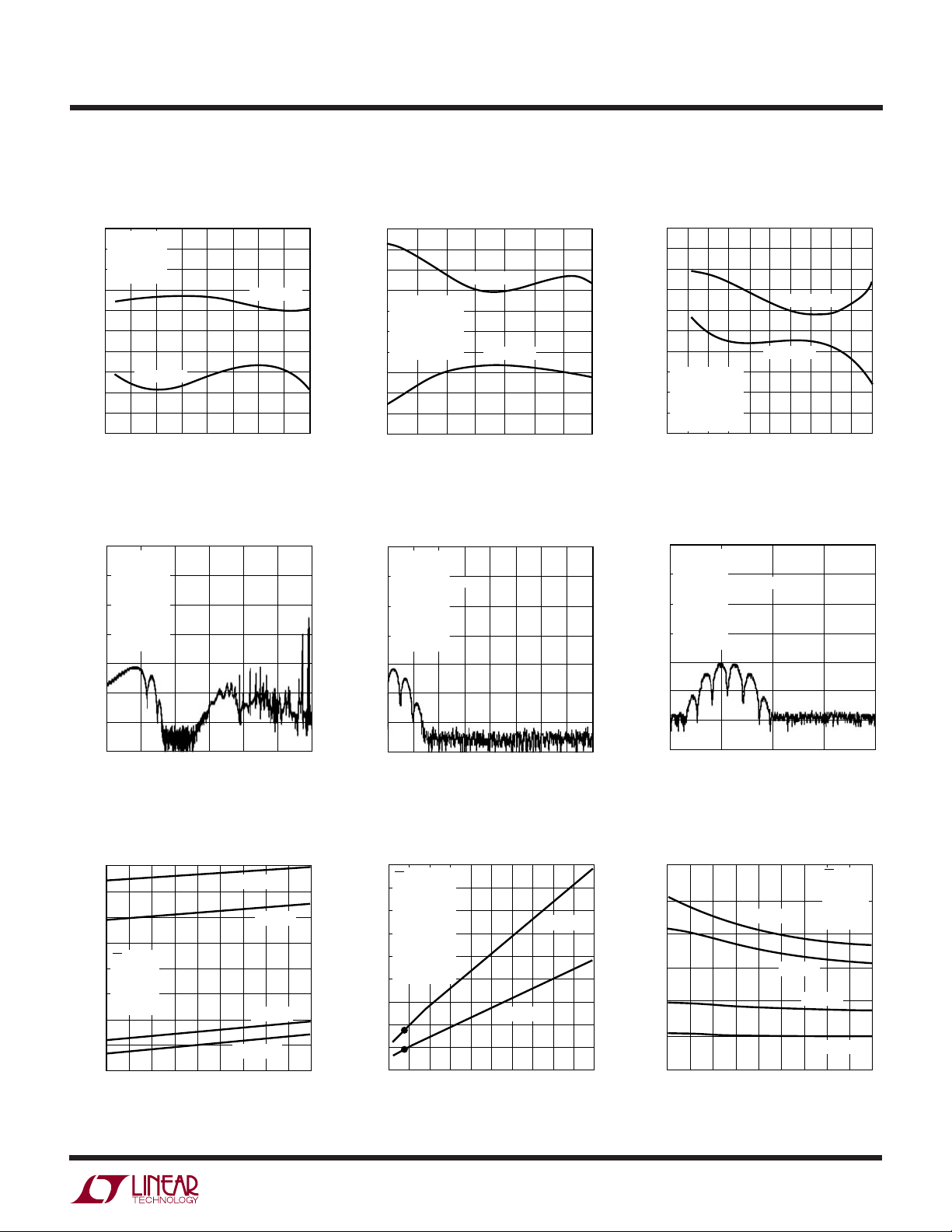
TYPICAL PERFOR A CE CHARACTERISTICS
LTC2414/LTC2418
Total Unadjusted Error
= 5V, V
(V
CC
3
FO = GND
= 5V
V
CC
= 5V
V
2
REF
= V
V
INCM
)
1
REF
0
–1
TUE (ppm OF V
–2
–3
–2.5 –2.0 –1.0 0 1.0 2.0
–1.5
= 5V)
REF
= 2.5V
REFCM
TA = 25°C
–0.5
INPUT VOLTAGE (V)
TA = –45°C
0.5 1.5
Integral Nonlinearity
= 5V, V
(V
CC
3
FO = GND
= 5V
V
CC
= 5V
V
2
REF
= V
V
INCM
)
1
REF
0
–1
INL (ppm OF V
–2
–3
–2.5 –2.0 –1.0 0 1.0 2.0
–1.5
= 5V)
REF
= 2.5V
REFCM
TA = 25°C
–0.5 0.5 1.5
INPUT VOLTAGE (V)
Noise Histogram
= 5V, V
(V
CC
30
10,000 CONSECUTIVE READINGS
= GND
F
O
= 25°C
T
25
A
= 5V
V
CC
= 5V
V
REF
20
= 0V
V
IN
= 2.5V
V
INCM
15
10
NUMBER OF READINGS (%)
5
REF
= 5V)
GAUSSIAN
DISTRIBUTION
m = –0.24ppm
σ = 0.183ppm
TA = 85°C
241418 G01
TA = 85°C
TA = –45°C
241418 G04
2.5
2.5
Total Unadjusted Error
(V
= 5V, V
CC
3
FO = GND
= 5V
V
CC
= 2.5V
V
2
REF
V
INCM
)
1
REF
0
TA = 85°C
–1
TUE (ppm OF V
–2
–3
–1.25
REF
= V
= 1.25V
REFCM
–0.25 0.25 0.75
–0.75
INPUT VOLTAGE (V)
Integral Nonlinearity
(VCC = 5V, V
3
FO = GND
= 5V
V
CC
V
2
REF
V
INCM
)
1
REF
0
–1
INL (ppm OF V
–2
–3
–1.25
= 2.5V
REF
= V
= 1.25V
REFCM
TA = 25°C
–0.25 0.25 0.75 1.25
–0.75
INPUT VOLTAGE (V)
Noise Histogram
(V
= 2.7V, V
CC
14
10,000 CONSECUTIVE READINGS
= GND
F
O
12
= 25°C
T
A
= 2.7V
V
CC
= 2.5V
V
10
REF
= 0V
V
IN
= 2.5V
V
INCM
8
6
4
NUMBER OF READINGS (%)
2
= 2.5V)
= 2.5V)
TA = 85°C
= 2.5V)
REF
TA = 25°C
TA = –45°C
241418 G02
TA = –45°C
241418 G05
GAUSSIAN
DISTRIBUTION
m = –0.48ppm
σ = 0.375ppm
1.25
Total Unadjusted Error
(V
= 2.7V, V
CC
8
FO = GND
= 2.7V
V
CC
6
= 2.5V
V
REF
V
INCM
4
)
REF
2
0
–2
TUE (ppm OF V
–4
–6
–8
–1.25
= V
–0.75
REF
= 1.25V
REFCM
TA = 25°C
–0.25 0.25 0.75
INPUT VOLTAGE (V)
Integral Nonlinearity
(V
= 2.7V, V
CC
8
FO = GND
= 2.7V
V
CC
6
V
REF
V
INCM
4
)
REF
2
0
–2
INL (ppm OF V
–4
–6
–8
–1.25
= 2.5V
= V
–0.75
REF
= 1.25V
REFCM
–0.25 0.25 0.75
INPUT VOLTAGE (V)
Long Term ADC Readings
1.0
RMS NOISE = 0.19ppm
= GND
F
O
= 25°C
T
A
)
0.5
= 5V
V
CC
REF
0
–0.5
ADC READING (ppm OF V
–1.0
V
V
V
REF
= 0V
IN
INCM
= 5V
= 2.5V
= 2.5V)
TA = –45°C
TA = 85°C
1.25
241418 G03
= 2.5V)
TA = –45°C
TA = 25°C
TA = 85°C
1.25
241418 G06
0
–1.2
–0.6 0
OUTPUT CODE (ppm OF V
REF
)
241418 G07
0.6
0
–2.4
–1.2 –0.6 0 0.6 1.2
–1.8
OUTPUT CODE (ppm OF V
REF
)
241418 G08
–1.5
0
20 30 40
10
TIME (HOURS)
50 60
LTXXXX • TPCXX
241418fa
7
LTC2414/LTC2418
UW
TYPICAL PERFOR A CE CHARACTERISTICS
RMS Noise vs Input Differential
)
REF
0.5
0.4
0.3
Voltage
FO = GND
= 25°C
T
A
= 5V
V
CC
= 5V
V
REF
= 2.5V
V
INCM
RMS Noise vs V
1.0
0.9
0.8
INCM
RMS Noise vs Temperature (TA)
1.2
1.1
1.0
0.9
0.2
RMS NOISE (ppm OF V
0.1
0
–2.5 –2.0 –1.0 0 1.0 2.0
–1.5
INPUT DIFFERENTIAL VOLTAGE (V)
RMS Noise vs V
1.0
0.9
0.8
0.7
RMS NOISE (µV)
0.6
0.5
2.7
3.1
3.5
–0.5
3.9
VCC (V)
0.5 1.5
CC
4.3
4.7
FO = GND
= 25°C
T
A
= 0V
V
IN
= GND
V
INCM
+
= 2.5V
REF
–
= GND
REF
5.1
241418 G10
241418 G13
5.5
2.5
0.7
RMS NOISE (µV)
0.6
0.5
–1
0
RMS Noise vs V
1.0
0.9
0.8
0.7
RMS NOISE (µV)
0.6
0.5
0
FO = GND
= 25°C
T
A
= 5V
V
CC
+
= 5V
REF
–
= GND
REF
= 0V
V
IN
= GND
V
INCM
1
V
INCM
4
(V)
3
2
5
241418 G11
6
REF
FO = GND
= 25°C
T
A
= 5V
V
CC
= 0V
V
IN
= GND
V
INCM
–
= GND
REF
1
3
4
2
V
(V)
REF
5
241418 G14
0.8
RMS NOISE (µV)
0.7
0.6
0.5
–50
0 25 50 75 100
–25
TEMPERATURE (°C)
Offset Error vs V
0
–0.1
)
–0.2
REF
–0.3
–0.4
–0.5
–0.6
–0.7
–0.8
OFFSET ERROR (ppm OF V
–0.9
–1.0
–1
1
0
V
2
INCM
INCM
3
(V)
FO = GND
= 5V
V
CC
= 5V
V
REF
= 0V
V
IN
= GND
V
INCM
FO = GND
= 25°C
T
A
= 5V
V
CC
+
= 5V
REF
–
REF
= 0V
V
IN
4
241418 G12
= GND
5
241418 G15
6
Offset Error vs Temperature
0
FO = GND
= 5V
V
CC
–0.1
)
REF
–0.2
–0.3
–0.4
–0.5
OFFSET ERROR (ppm OF V
–0.6
–0.7
V
REF
= 0V
V
IN
V
INCM
–45 –30
= 5V
= GND
–15 0 7545
15 30 60 90
TEMPERATURE (°C)
8
241418 G16
Offset Error vs V
1.0
FO = GND
0.8
= 25°C
T
A
= 0V
V
)
IN
0.6
REF
0.4
0.2
–0.2
–0.4
–0.6
OFFSET ERROR (ppm OF V
–0.8
–1.0
= GND
V
INCM
+
= 2.5V
REF
–
= GND
REF
0
3.1
3.5
2.7
3.9
VCC (V)
CC
4.3
4.7
5.1
241418 G17
5.5
Offset Error vs V
1.0
FO = GND
0.8
= 25°C
T
A
)
REF
–0.2
–0.4
–0.6
OFFSET ERROR (ppm OF V
–0.8
–1.0
0.6
0.4
0.2
= 5V
V
CC
= 0V
V
IN
= GND
V
INCM
–
= GND
REF
0
1
0
REF
3
4
2
V
(V)
REF
5
241418 G18
241418fa
UW
TYPICAL PERFOR A CE CHARACTERISTICS
LTC2414/LTC2418
Full-Scale Error vs Temperature
5
FO = GND
4
= 5V
V
CC
)
REF
FULL-SCALE ERROR (ppm OF V
3
2
1
0
–1
–2
–3
–4
–5
–60
= 5V
V
REF
= 2.5V
V
INCM
–FS ERROR
–40 0
–20
20
TEMPERATURE (°C)
40
PSRR vs Frequency at V
0
FO = GND
= 25°C
T
A
–20
= 4.1V
V
CC
DC
REF+ = 2.5V
–
–40
–60
–80
REJECTION (dB)
–100
= GND
REF
+
= GND
IN
–
= GND
IN
SDI = GND
+FS ERROR
80
60
241418 G19
CC
100
Full-Scale Error vs V
5
4
)
REF
3
2
FO = GND
1
= 25°C
T
A
= 2.5V
V
REF
0
= 0.5V
V
INCM
–1
REF– = GND
–2
–3
FULL-SCALE ERROR (ppm OF V
–4
–5
2.7
3.1
+FS ERROR
REF
3.5 3.9 4.3 4.7 5.1 5.5
VCC (V)
PSRR vs Frequency at V
0
FO = GND
= 25°C
T
A
–20
V
CC
REF
–40
REF
+
IN
–
IN
–60
SDI = GND
–80
REJECTION (dB)
–100
= 4.1V
+
= 2.5V
–
= GND
= GND
= GND
DC
±1.4V
CC
–FS ERROR
CC
241418 G20
Full-Scale Error vs V
5
4
)
REF
3
2
1
0
–1
–2
FO = GND
= 25°C
T
A
–3
= 5V
V
CC
FULL-SCALE ERROR (ppm OF V
–4
–5
= 0.5V
V
INCM
REF– = GND
0
0.5
REF
1.0 1.5 2.0 2.5 3.0 3.5 4.0 4.5 5.0
V
REF
PSRR vs Frequency at V
0
FO = GND
= 25°C
T
A
–20
V
CC
REF+ = 2.5V
–40
REF
+
IN
–
IN
–60
SDI = GND
–80
REJECTION (dB)
–100
= 4.1V
–
= GND
= GND
= GND
DC
±0.7V
P-P
REF
+FS ERROR
–FS ERROR
(V)
241418 G21
CC
–120
–140
1
10
FREQUENCY AT VCC (Hz)
Conversion Current
vs Temperature
240
230
220
210
CS = GND
200
= GND
F
O
SCK = NC
190
SDO = NC
SDI = GND
180
CONVERSION CURRENT (µA)
170
160
–45 –30 –15
100 1000 10000 100000 1000000
241418 G22
VCC = 5.5V
VCC = 5V
VCC = 3V
VCC = 2.7V
15 30
0
TEMPERATURE (°C)
756045
241418 G25
90
–120
–140
30 90 150 210
0
60 120 240
FREQUENCY AT VCC (Hz)
Supply Current at Elevated
Output Rates (FO Over Driven)
1000
CS = GND
900
= EXT OSC
F
O
+
= GND
IN
–
800
= GND
IN
SCK = NC
700
SDO = NC
SDI = GND
600
= 25°C
T
A
= V
V
REF
500
400
SUPPLY CURRENT (µA)
300
200
100
CC
0 102030
OUTPUT DATA RATE (READINGS/SEC)
40
50
180
241418 G23
VCC = 5V
VCC = 3V
60 70 80 90 100
241418 G26
–120
–140
15250 15300 15350 15400 15450
FREQUENCY AT V
(Hz)
CC
Sleep Mode Current
vs Temperature
6
5
4
3
2
SLEEP-MODE CURRENT (µA)
1
0
–45 –30 –15
VCC = 5.5V
15 30
0
TEMPERATURE (°C)
VCC = 5V
VCC = 3V
CS = V
FO = GND
SCK = NC
SDO = NC
SDI = GND
VCC = 2.7V
241418 G24
CC
756045
241418 G27
241418fa
90
9

LTC2414/LTC2418
U
UU
PI FU CTIO S
CH0 to CH15 (Pin 21 to Pin 28 and Pin 1 to Pin 8): Analog
Inputs. May be programmed for single-ended or differential mode. CH8 to CH15 (Pin 1 to Pin 8) not connected on
the LTC2414.
V
(Pin 9): Positive Supply Voltage. Bypass to GND
CC
(Pin 15) with a 10µF tantalum capacitor in parallel with
0.1µF ceramic capacitor as close to the part as possible.
COM (Pin 10): The common negative input (IN–) for all
single-ended multiplexer configurations. The voltage on
Channel 0 to 15 and COM input pins can have any value
between GND – 0.3V and V
the two selected inputs (IN
input range (V
= IN+ – IN–) from – 0.5 • V
IN
Outside this input range, the converter produces unique
overrange and underrange output codes.
REF+ (Pin 11), REF– (Pin 12): Differential Reference
Input. The voltage on these pins can have any value
between GND and V
input, REF
+
, is maintained more positive than the negative
reference input, REF
CC
–
, by at least 0.1V.
GND (Pin 15): Ground. Connect this pin to a ground plane
through a low impedance connection.
CS (Pin 16): Active LOW Digital Input. A LOW on this pin
enables the SDO digital output and wakes up the ADC.
Following each conversion the ADC automatically enters
the Sleep mode and remains in this low power state as
long as CS is HIGH. A LOW-to-HIGH transition on CS
during the Data Output transfer aborts the data transfer
and starts a new conversion.
SDO (Pin 17): Three-State Digital Output. During the Data
Output period, this pin is used as the serial data output.
When the chip select CS is HIGH (CS = V
+ 0.3V. Within these limits,
CC
+
and IN–) provide a bipolar
to 0.5 • V
REF
REF
.
as long as the positive reference
), the SDO pin
CC
is in a high impedance state. During the Conversion and
Sleep periods, this pin is used as the conversion status
output. The conversion status can be observed by pulling
CS LOW.
SCK (Pin 18): Bidirectional Digital Clock Pin. In Internal
Serial Clock Operation mode, SCK is used as the digital
output for the internal serial interface clock during the Data
Output period. In External Serial Clock Operation mode,
SCK is used as the digital input for the external serial
interface clock during the Data Output period. A weak
internal pull-up is automatically activated in Internal Serial
Clock Operation mode. The Serial Clock Operation mode is
determined by the logic level applied to the SCK pin at
power up or during the most recent falling edge of CS.
(Pin 19): Frequency Control Pin. Digital input that
F
O
controls the ADC’s notch frequencies and conversion
time. When the F
pin is connected to VCC (FO = VCC), the
O
converter uses its internal oscillator and the digital filter
first null is located at 50Hz. When the F
to GND (F
= 0V), the converter uses its internal oscillator
O
and the digital filter first null is located at 60Hz. When F
is driven by an external clock signal with a frequency f
pin is connected
O
EOSC
O
,
the converters use this signal as their system clock and the
digital filter first null is located at a frequency f
EOSC
/2560.
SDI (Pin 20): Serial Digital Data Input. During the Data
Output period, this pin is used to shift in the multiplexer
address started from the first rising SCK edge. During the
Conversion and Sleep periods, this pin is in the DON’T
CARE state. However, a HIGH or LOW logic level should be
maintained on SDI in the DON’T CARE mode to avoid an
excessive current in the SDI input buffers.
NC Pins: Do Not Connect.
10
241418fa
LTC2414/LTC2418
1.69k
SDO
241418 TA03
Hi-Z TO V
OL
VOH TO V
OL
VOL TO Hi-Z
C
LOAD
= 20pF
V
CC
UU
W
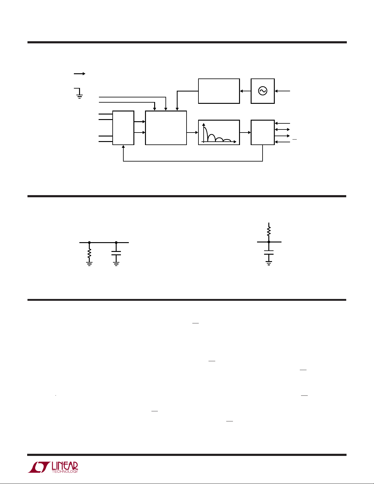
FU CTIO AL BLOCK DIAGRA
V
CC
GND
+
REF
–
REF
CH0
CH1
CH15
COM
•
•
MUX
•
+
IN
–
IN
–
DIFFERENTIAL
3RD ORDER
∆Σ MODULATOR
TEST CIRCUITS
+
Figure 1
AUTOCALIBRATION
AND CONTROL
DECIMATING FIR
ADDRESS
INTERNAL
OSCILLATOR
SERIAL
INTERFACE
241418 F01
F
O
(INT/EXT)
SDI
SCK
SDO
CS
SDO
1.69k
Hi-Z TO V
VOL TO V
OH
VOH TO Hi-Z
OH
C
LOAD
241418 TA02
= 20pF
WUUU
APPLICATIO S I FOR ATIO
CONVERTER OPERATION
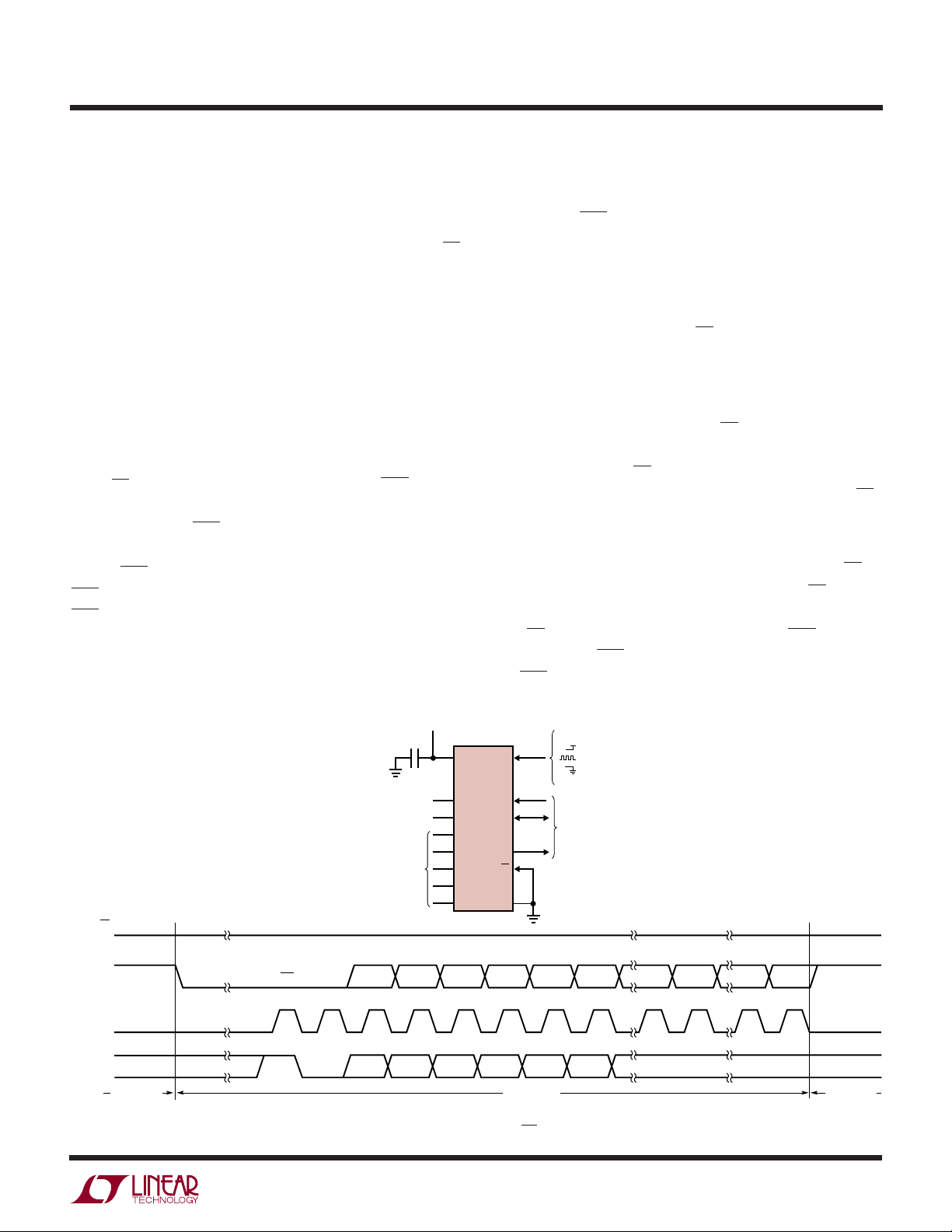
Converter Operation Cycle
The LTC2414/LTC2418 are multichannel, low power, deltasigma analog-to-digital converters with an easy-to-use
4-wire serial interface (see Figure 1). Their operation is made
up of three states. The converter operating cycle begins with
the conversion, followed by the low power sleep state and
ends with the data input/output (see Figure 2). The 4-wire
interface consists of serial data input (SDI), serial data output (SDO), serial clock (SCK) and chip select (CS).
Initially, the LTC2414 or LTC2418 performs a conversion.
Once the conversion is complete, the device enters the
sleep state. The part remains in the sleep state as long as
CS is HIGH. While in the sleep state, power consumption
is reduced by nearly two orders of magnitude. The conversion result is held indefinitely in a static shift register while
the converter is in the sleep state.
Once CS is pulled LOW, the device exits the low power
mode and enters the data output state. If CS is pulled HIGH
before the first rising edge of SCK, the device returns to the
low power sleep mode and the conversion result is still
held in the internal static shift register. If CS remains LOW
after the first rising edge of SCK, the device begins outputting the conversion result and inputting channel selection
bits. Taking CS high at this point will terminate the data
output state and start a new conversion. The channel
selection control bits are shifted in through SDI from the
241418fa
11
LTC2414/LTC2418
WUUU
APPLICATIO S I FOR ATIO
POWER UP
+
= CH0, IN– = CH1
IN
CONVERT
SLEEP
FALSE
CS = LOW
AND
SCK
TRUE
DATA OUTPUT
ADDRESS INPUT
Figure 2. LTC2414/LTC2418 State Transition Diagram
241418 F02
first rising edge of SCK and depending on the control bits,
the converter updates its channel selection immediately
and is valid for the next conversion. The details of channel
selection control bits are described in the Input Data Mode
section. The output data is shifted out the SDO pin under
the control of the serial clock (SCK). The output data is
updated on the falling edge of SCK allowing the user to
reliably latch data on the rising edge of SCK (see Figure 3).
The data output state is concluded once 32 bits are read
out of the ADC or when CS is brought HIGH. The device
automatically initiates a new conversion and the cycle
repeats.
Through timing control of the CS and SCK pins, the
LTC2414/LTC2418 offer several flexible modes of operation (internal or external SCK and free-running conversion
modes). These various modes do not require programming configuration registers; moreover, they do not disturb the cyclic operation described above. These modes of
operation are described in detail in the Serial Interface
Timing Modes section.
Conversion Clock
A major advantage the delta-sigma converter offers over
conventional type converters is an on-chip digital filter
(commonly implemented as a Sinc or Comb filter). For
high resolution, low frequency applications, this filter is
typically designed to reject line frequencies of 50Hz or
60Hz plus their harmonics. The filter rejection performance is directly related to the accuracy of the converter
system clock. The LTC2414/LTC2418 incorporate a highly
accurate on-chip oscillator. This eliminates the need for
external frequency setting components such as crystals or
oscillators. Clocked by the on-chip oscillator, the
LTC2418
achieve a minimum of 110dB rejection at the line
LTC2414/
frequency (50Hz or 60Hz ± 2%).
Ease of Use
The LTC2414/LTC2418 data output has no latency, filter
settling delay or redundant data associated with the
conversion cycle. There is a one-to-one correspondence
between the conversion and the output data. Therefore,
multiplexing multiple analog voltages is easy.
The LTC2414/LTC2418 perform offset and full-scale calibrations in every conversion cycle. This calibration is transparent to the user and has no effect on the cyclic operation
described above. The advantage of continuous calibration
is extreme stability of offset and full-scale readings with respect to time, supply voltage change and temperature drift.
Power-Up Sequence
The LTC2414/LTC2418 automatically enter an internal
reset state when the power supply voltage V
drops
CC
below approximately 2V. This feature guarantees the
integrity of the conversion result and of the serial interface
mode selection. (See the 3-wire I/O sections in the Serial
Interface Timing Modes section.)
When the V
voltage rises above this critical threshold,
CC
the converter creates an internal power-on-reset (POR)
signal with a typical duration of 1ms. The POR signal
clears all internal registers. Following the POR signal, the
LTC2414/LTC2418 start a normal conversion cycle and
follow the succession of states described above. The first
conversion result following POR is accurate within the
specifications of the device if the power supply voltage is
restored within the operating range (2.7V to 5.5V) before
the end of the POR time interval.
Reference Voltage Range
The LTC2414/LTC2418 accept a truly differential external
reference voltage. The absolute/common mode voltage
241418fa
12

WUUU
APPLICATIO S I FOR ATIO
LTC2414/LTC2418
specification for the REF+ and REF– pins covers the entire
range from GND to V
+
the REF
pin must always be more positive than the REF
. For correct converter operation,
CC
–
pin.
The LTC2414/LTC2418 can accept a differential reference
voltage from 0.1V to V
. The converter output noise is
CC
determined by the thermal noise of the front-end circuits,
and, as such, its value in nanovolts is nearly constant with
reference voltage. A decrease in reference voltage will not
significantly improve the converter’s effective resolution.
On the other hand, a reduced reference voltage will improve the converter’s overall INL performance. A reduced
reference voltage will also improve the converter performance when operated with an external conversion clock
(external FO signal) at substantially higher output data rates.
Input Voltage Range
The two selected pins are labeled IN
+
and IN– (see Tables
1 and 2). Once selected (either differential or single-ended
multiplexing mode), the analog input is differential with a
common mode range for the IN+ and IN– input pins extending from GND – 0.3V to V
+ 0.3V. Outside
CC
these limits, the ESD protection devices begin to turn on
and the errors due to input leakage current increase rapidly. Within these limits, the LTC2414/LTC2418 convert
the bipolar differential input signal, V
– FS = – 0.5 • V
+
REF
– REF–. Outside this range the converters indicate
to +FS = 0.5 • V
REF
= IN+ – IN–, from
IN
where V
REF
REF
=
the overrange or the underrange condition using distinct
output codes.
Input signals applied to IN+ and IN– pins may extend
300mV below ground or above VCC. In order to limit any
fault current, resistors of up to 5k may be added in series
with the IN+ or IN– pins without affecting the performance
of the device. In the physical layout, it is important to
maintain the parasitic capacitance of the connection between these series resistors and the corresponding pins
as low as possible; therefore, the resistors should be
located as close as practical to the pins. In addition, series
resistors will introduce a temperature dependent offset
error due to the input leakage current. A 1nA input leakage
current will develop a 1ppm offset error on a 5k resistor if
V
= 5V. This error has a very strong temperature
REF
dependency.
Input Data Format
When the LTC2414/LTC2418 are powered up, the default
selection used for the first conversion is IN
+
= CH0 and IN
–
= CH1 (Address = 00000). In the data input/output mode
following the first conversion, a channel selection can be
updated using an 8-bit word. The LTC2414/LTC2418
serial input data is clocked into the SDI pin on the rising
edge of SCK (see Figure 3). The input is composed of an
8-bit word with the first 3 bits acting as control bits and the
remaining 5 bits as the channel address bits.
The first 2 bits are always 10 for proper updating operation. The third bit is EN. For EN = 1, the following 5 bits are
used to update the input channel selection. For EN = 0,
previous channel selection is kept and the following bits
are ignored. Therefore, the address is updated when the 3
control bits are 101 and kept for 100. Alternatively, the 3
control bits can be all zero to keep the previous address.
This alternation is intended to simplify the SDI interface
allowing the user to simply connect SDI to ground if no
update is needed. Combinations other than 101, 100 and
000 of the 3 control bits should be avoided.
When update operation is set (101), the following 5 bits
are the channel address. The first bit, SGL, decides if the
differential selection mode (SGL = 0) or the single-ended
selection mode is used (SGL = 1). For SGL = 0, two
adjacent channels can be selected to form a differential
input; for SGL = 1, one of the 8 channels (CH0-CH7) for the
LTC2414 or one of the 16 channels (CH0-CH15) for the
LTC2418 is selected as the positive input and the COM pin
is used as the negative input. For the LTC2414, the lower
half channels (CH0-CH7) are used and the channel address bit A2 should be always 0, see Table 1. While for the
LTC2418, all the 16 channels are used and the size of the
corresponding selection table (Table 2) is doubled from
that of the LTC2414 (Table 1). For a given channel selection, the converter will measure the voltage between the
two channels indicated by IN
+
and IN– in the selected row
of Tables 1 or 2.
241418fa
13
LTC2414/LTC2418
WUUU
APPLICATIO S I FOR ATIO
CS
BIT31
SDO
SCK
SDI
SLEEP DATA INPUT/OUTPUT
Hi-Z
EOC
1 0 EN SGL A2 A1 A0 DON’T CARE
BIT29
BIT28 BIT27 BIT26 BIT25 BIT24
SIGDMY
MSB B22
CONVERSON RESULT
ODD/
SIGN
Figure 3a. Input/Output Data Timing
CONVERSION RESULT
SDO
SCK
SDI
OPERATION
N – 1
ADDRESS
N – 1
ADDRESS
N
OUTPUT
N – 1
Hi-Z
DON’T CARE
CONVERSION N
CONVERSION RESULT
ADDRESS
ADDRESS
OUTPUT
Figure 3b. Typical Operation Sequence
N
N
N + 1
N
BIT6
LSB
DON’T CARE
CONVERSION N + 1
BIT4BIT30
BIT5
ODD/
SGL
SIGN
ADDRESS CORRESPONDING TO RESULT
CONVERSION RESULT
Hi-Z Hi-Z
BIT3A1BIT2A0BIT1
A2
N + 1
ADDRESS
N + 1
ADDRESS
N + 2
OUTPUT
N + 1
241418 F03b
BIT0
PARITY
CONVERSION
241418 F03a
Table 1. Channel Selection for the LTC2414 (Bit A2 Should Always Be 0)
MUX ADDRESS CHANNEL SELECTION
ODD/
SGL SIGN A2 A1 A0 01234567COM
*0 0 000 IN+IN
0 0 001 IN+IN
0 0 010 IN+IN
0 0 011 IN+IN
0 1 000 IN–IN
0 1 001 IN–IN
0 1 010 IN–IN
0 1 011 IN–IN
1 0 000 IN
1 0 001 IN
1 0 010 IN
1 0 011 IN
1 1 000 IN
1 1 001 IN
1 1 010 IN
1 1 011 IN+IN
*Default at power up
–
–
–
–
+
+
+
+
+
+
+
+
+
+
+
IN
IN
IN
IN
IN
IN
IN
–
–
–
–
–
–
–
–
241418fa
14
LTC2414/LTC2418
WUUU
APPLICATIO S I FOR ATIO
Table 2. Channel Selection for the LTC2418
MUX ADDRESS CHANNEL SELECTION
ODD/
SGL SIGN A2 A1 A0 0 123456789101112131415COM
*00000IN+IN
00001 IN+IN
00010 IN+IN
00011 IN+IN
00100 IN+IN
00101 IN+IN
00110 IN+IN
00111 IN+IN
01000IN–IN
01001 IN–IN
01010 IN–IN
01011 IN–IN
01100 IN–IN
01101 IN–IN
01110 IN–IN
01111 IN–IN
10000IN
10001 IN
10010 IN
10011 IN
10100 IN
10101 IN
10110 IN
10111 IN
11000 IN
11001 IN
11010 IN
11011 IN
11100 IN
11101 IN
11110 IN
11111 IN+IN
*Default at power up
–
–
–
–
–
–
–
–
+
+
+
+
+
+
+
+
+
+
+
+
+
+
+
+
+
+
+
+
+
+
+
–
IN
–
IN
–
IN
–
IN
–
IN
–
IN
–
IN
–
IN
–
IN
–
IN
–
IN
–
IN
–
IN
–
IN
–
IN
–
Output Data Format
The LTC2414/LTC2418 serial output data stream is 32 bits
long. The first 3 bits represent status information indicating the sign and conversion state. The next 23 bits are the
conversion result, MSB first. The next 5 bits (Bit 5 to Bit 1)
indicate which channel the conversion just performed was
selected. The address bits programmed during this data
output phase select the input channel for the next conversion cycle. These address bits are output during the subsequent data read, as shown in Figure 3b. The last bit is a
241418fa
15

LTC2414/LTC2418
WUUU
APPLICATIO S I FOR ATIO
parity bit representing the parity of the previous 31 bits. The
parity bit is useful to check the output data integrity especially when the output data is transmitted over a distance.
The third and fourth bits together are also used to indicate
an underrange condition (the differential input voltage is below –FS) or an overrange condition (the differential input
voltage is above +FS).
Bit 31 (first output bit) is the end of conversion (EOC)
indicator. This bit is available at the SDO pin during the
conversion and sleep states whenever the CS pin is LOW.
This bit is HIGH during the conversion and goes LOW
when the conversion is complete.
Bit 30 (second output bit) is a dummy bit (DMY) and is
always LOW.
Bit 29 (third output bit) is the conversion result sign indicator (SIG). If V
is >0, this bit is HIGH. If VIN is <0, this
IN
bit is LOW.
Bit 28 (fourth output bit) is the most significant bit (MSB)
of the result. This bit in conjunction with Bit 29 also
provides the underrange or overrange indication. If both
Bit 29 and Bit 28 are HIGH, the differential input voltage is
above +FS. If both Bit 29 and Bit 28 are LOW, the
differential input voltage is below –FS.
The function of these bits is summarized in Table 3.
Table 3. LTC2414/LTC2418 Status Bits
Bit 31 Bit 30 Bit 29 Bit 28
Input Range EOC DMY SIG MSB
VIN ≥ 0.5 • V
0V ≤ VIN < 0.5 • V
–0.5 • V
VIN < –0.5 • V
REF
≤ VIN < 0V 0 0 0 1
REF
REF
REF
0011
0010
0000
Bits 28-6 are the 23-bit conversion result MSB first.
Bit 6 is the least significant bit (LSB).
Bits 5-1 are the corresponding channel selection bits for
the present conversion result with bit SGL output first as
shown in Figure 3.
Bit 0 is the parity bit representing the parity of the previous
31 bits. Including the parity bit, the total numbers of 1’s
and 0’s in the output data are always even.
Data is shifted out of the SDO pin under control of the serial
clock (SCK), see Figure 3. Whenever CS is HIGH, SDO
remains high impedance and any externally generated
SCK clock pulses are ignored by the internal data out shift
register.
In order to shift the conversion result out of the device, CS
must first be driven LOW. EOC is seen at the SDO pin of the
device once CS is pulled LOW. EOC changes real time from
HIGH to LOW at the completion of a conversion. This
signal may be used as an interrupt for an external microcontroller. Bit 31 (EOC) can be captured on the first rising
edge of SCK. Bit 30 is shifted out of the device on the first
falling edge of SCK. The final data bit (Bit 0) is shifted out
on the falling edge of the 31st SCK and may be latched on
the rising edge of the 32nd SCK pulse. On the falling edge
of the 32nd SCK pulse, SDO goes HIGH indicating the
initiation of a new conversion cycle. This bit serves as EOC
(Bit 31) for the next conversion cycle. Table 4 summarizes
the output data format.
As long as the voltage applied to any channel (CH0-CH15,
COM) is maintained within the –0.3V to (V
+ 0.3V)
CC
absolute maximum operating range, a conversion result is
generated for any differential input voltage V
–FS = – 0.5 • V
to +FS = 0.5 • V
REF
. For differential input
REF
from
IN
voltages greater than + FS, the conversion result is clamped
to the value corresponding to the +FS + 1LSB. For differential input voltages below –FS, the conversion result is
clamped to the value corresponding to –FS – 1LSB.
Frequency Rejection Selection (F
)
O
The LTC2414/LTC2418 internal oscillator provides better
than 110dB normal mode rejection at the line frequency
and all its harmonics for 50Hz ± 2% or 60Hz ± 2%. For
60Hz rejection, F
50Hz rejection the F
should be connected to GND while for
O
pin should be connected to VCC.
O
The selection of 50Hz or 60Hz rejection can also be made
by driving F
to an appropriate logic level. A selection
O
change during the sleep or data output states will not
disturb the converter operation. If the selection is made
during the conversion state, the result of the conversion in
progress may be outside specifications but the following
conversions will not be affected.
16
241418fa

WUUU
APPLICATIO S I FOR ATIO
Table 4. LTC2414/LTC2418 Output Data Format
Differential Input Voltage Bit 31 Bit 30 Bit 29 Bit 28 Bit 27 Bit 26 Bit 25 … Bit 6
VIN* EOC DMY SIG MSB LSB
VIN* ≥ 0.5 • V
0.5 • V
REF
0.25 • V
REF
0.25 • V
REF
0 0 0100 0 0…0
–1LSB 0 0011 1 1…1
– 0.25 • V
– 0.25 • V
– 0.5 • V
VIN* < –0.5 • V
*The differential input voltage VIN = IN+ – IN–.
**The differential reference voltage V
** 0 0110 0 0…0
REF
** – 1LSB 0 0101 1 1…1
** 0 0101 0 0…0
** – 1LSB 0 0100 1 1…1
** 0 0011 0 0…0
REF
** – 1LSB 00010 1 1…1
REF
** 0 0010 0 0…0
REF
** 0 0001 1 1…1
REF
= REF+ – REF–.
REF
LTC2414/LTC2418
When a fundamental rejection frequency different from
50Hz or 60Hz is required or when the converter must be
synchronized with an outside source, the LTC2414/
LTC2418 can operate with an external conversion clock.
The converter automatically detects the presence of an
external clock signal at the F
oscillator. The frequency f
pin and turns off the internal
O
of the external signal must
EOSC
be at least 2560Hz (1Hz notch frequency) to be detected.
The external clock signal duty cycle is not significant as
long as the minimum and maximum specifications for the
high and low periods t
HEO
and t
are observed.
LEO
While operating with an external conversion clock of a
frequency f
normal mode rejection in a frequency range f
, the converter provides better than 110dB
EOSC
EOSC
/2560
± 4% and its harmonics. The normal mode rejection as a
function of the input frequency deviation from f
EOSC
/2560
is shown in Figure 4.
Whenever an external clock is not present at the F
pin, the
O
converter automatically activates its internal oscillator and
enters the Internal Conversion Clock mode. The converter
operation will not be disturbed if the change of conversion
clock source occurs during the sleep state or during the
data output state while the converter uses an external
serial clock. If the change occurs during the conversion
state, the result of the conversion in progress may be
outside specifications but the following conversions will
not be affected. If the change occurs during the data output
state and the converter is in the Internal SCK mode, the
–80
–85
–90
–95
–100
–105
–110
–115
–120
–125
NORMAL MODE REJECTION (dB)
–130
–135
–140
–12–8–404812
DIFFERENTIAL INPUT SIGNAL FREQUENCY
DEVIATION FROM NOTCH FREQUENCY f
Figure 4. LTC2414/LTC2418 Normal Mode Rejection
When Using an External Oscillator of Frequency f
EOSC
/2560(%)
241418 F04
EOSC
serial clock duty cycle may be affected but the serial data
stream will remain valid.
Table 5 summarizes the duration of each state and the
achievable output data rate as a function of F
.
O
SERIAL INTERFACE PINS
The LTC2414/LTC2418 transmit the conversion results
and receive the start of conversion command through a
synchronous 4-wire interface. During the conversion and
sleep states, this interface can be used to assess the converter status and during the data I/O state it is used to read
the conversion result and write in channel selection bits.
241418fa
17

LTC2414/LTC2418
WUUU
APPLICATIO S I FOR ATIO
Table 5. LTC2414/LTC2418 State Duration
State Operating Mode Duration
CONVERT Internal Oscillator FO = LOW 133ms, Output Data Rate ≤ 7.5 Readings/s
(60Hz Rejection)
FO = HIGH 160ms, Output Data Rate ≤ 6.2 Readings/s
(50Hz Rejection)
External Oscillator FO = External Oscillator 20510/f
with Frequency f
(f
/2560 Rejection)
EOSC
SLEEP As Long As CS = HIGH Until CS = LOW and SCK
DATA OUTPUT Internal Serial Clock FO = LOW/HIGH As Long As CS = LOW But Not Longer Than 1.67ms
(Internal Oscillator) (32 SCK cycles)
FO = External Oscillator with As Long As CS = LOW But Not Longer Than 256/f
Frequency f
External Serial Clock with As Long As CS = LOW But Not Longer Than 32/f
Frequency f
kHz (32 SCK cycles)
SCK
EOSC
kHz
EOSC
kHz (32 SCK cycles)
s, Output Data Rate ≤ f
EOSC
/20510 Readings/s
EOSC
SCK
EOSC
ms
ms
Serial Clock Input/Output (SCK)
The serial clock signal present on SCK (Pin 18) is used to
synchronize the data transfer. Each bit of data is shifted out
the SDO pin on the falling edge of the serial clock and each
input bit is shifted in the SDI pin on the rising edge of the
serial clock.
In the Internal SCK mode of operation, the SCK pin is an
output and the LTC2414/LTC2418 create their own serial
clock by dividing the internal conversion clock by 8. In the
External SCK mode of operation, the SCK pin is used as
input. The internal or external SCK mode is selected on
power-up and then reselected every time a HIGH-to-LOW
transition is detected at the CS pin. If SCK is HIGH or floating at power-up or during this transition, the converter
enters the internal SCK mode. If SCK is LOW at power-up
or during this transition, the converter enters the external
SCK mode.
Serial Data Input (SDI)
The serial data input pin, SDI (Pin 20), is used to shift in the
channel control bits during the data output state to prepare
the channel selection for the following conversion.
When CS (Pin 16) is HIGH or the converter is in the conversion state, the SDI input is ignored and may be driven
HIGH or LOW. When CS goes LOW and the conversion is
complete, SDO goes low and then SDI starts to shift in bits
on the rising edge of SCK.
Serial Data Output (SDO)
The serial data output pin, SDO (Pin 17), provides the
result of the last conversion as a serial bit stream (MSB
first) during the data output state. In addition, the SDO pin
is used as an end of conversion indicator during the
conversion and sleep states.
When CS (Pin 16) is HIGH, the SDO driver is switched to
a high impedance state. This allows sharing the serial
interface with other devices. If CS is LOW during the
convert or sleep state, SDO will output EOC. If CS is LOW
during the conversion phase, the EOC bit appears HIGH on
the SDO pin. Once the conversion is complete, EOC goes
LOW. The device remains in the sleep state until the first
rising edge of SCK occurs while CS = LOW.
Chip Select Input (CS)
The active LOW chip select, CS (Pin 16), is used to test the
conversion status and to enable the data input/output
transfer as described in the previous sections.
In addition, the CS signal can be used to trigger a new
conversion cycle before the entire serial data transfer has
been completed. The LTC2414/LTC2418 will abort any
serial data transfer in progress and start a new conversion
cycle anytime a LOW-to-HIGH transition is detected at the
CS pin after the converter has entered the data input/
output state (i.e., after the first rising edge of SCK occurs
with CS = LOW). If the device has not finished loading the
241418fa
18

WUUU
APPLICATIO S I FOR ATIO
LTC2414/LTC2418
last input bit A0 of SDI by the time CS pulled HIGH, the
address information is discarded and the previous
address is kept.
Finally, CS can be used to control the free-running modes
of operation, see Serial Interface Timing Modes section.
Grounding CS will force the ADC to continuously convert
at the maximum output rate selected by F
.
O
nal serial clock, 3- or 4-wire I/O, single cycle conversion.
The following sections describe each of these serial interface timing modes in detail. In all these cases, the converter can use the internal oscillator (F
= LOW or FO =
O
HIGH) or an external oscillator connected to the F
Refer to Table 6 for a summary.
External Serial Clock, Single Cycle Operation
(SPI/MICROWIRE Compatible)
SERIAL INTERFACE TIMING MODES
This timing mode uses an external serial clock to shift out
The LTC2414/LTC2418’s 4-wire interface is SPI and
MICROWIRE compatible. This interface offers several
the conversion result and a CS signal to monitor and
control the state of the conversion cycle, see Figure 5.
flexible modes of operation. These include internal/exter-
Table 6. LTC2414/LTC2418 Interface Timing Modes
Conversion Data Connection
SCK Cycle Output and
Configuration Source Control Control Waveforms
External SCK, Single Cycle Conversion External CS and SCK CS and SCK Figures 5, 6
External SCK, 3-Wire I/O External SCK SCK Figure 7
Internal SCK, Single Cycle Conversion Internal CS ↓ CS ↓ Figures 8, 9
Internal SCK, 3-Wire I/O, Continuous Conversion Internal Continuous Internal Figure 10
pin.
O
SDO
SCK
(EXTERNAL)
SDI
CS
TEST EOC
CONVERSION
TEST EOC
(OPTIONAL)
DON’T CARE
2.7V TO 5.5V
1µF
919
V
F
CC
O
LTC2414/
LTC2418
11
REFERENCE
VOLTAGE
0.1V TO V
CC
ANALOG
INPUTS
BIT 31
EOC
(1) (0) EN SGL A2 A1 A0
SLEEPSLEEP
+
REF
REF
CH0
CH7
CH8
CH15
COM
SDI
–
SCK
•
•
•
•
•
•
17
SDO
CS
15
GND
DATA OUTPUT CONVERSION
12
21
•
•
•
28
1
•
•
•
8
10
ODD/
SIGN
20
18
16
V
CC
= 50Hz REJECTION
= EXTERNAL OSCILLATOR
= 60Hz REJECTION
4-WIRE
SPI INTERFACE
BIT 6BIT 27 BIT 26 BIT 25 BIT 24BIT 28BIT 29BIT 30
LSB
DON’T CARE
BIT 0
PARITYMSBSIG
TEST EOC
Hi-ZHi-ZHi-Z
241418 F05
Figure 5. External Serial Clock, Single Cycle Operation
241418fa
19

LTC2414/LTC2418
WUUU
APPLICATIO S I FOR ATIO
The serial clock mode is selected on the falling edge of CS.
To select the external serial clock mode, the serial clock pin
(SCK) must be LOW during each CS falling edge.
The serial data output pin (SDO) is Hi-Z as long as CS is
HIGH. At any time during the conversion cycle, CS may be
pulled LOW in order to monitor the state of the converter.
While CS is pulled LOW, EOC is output to the SDO pin.
EOC = 1 while a conversion is in progress and EOC = 0 if
the device is in the sleep state. Independent of CS, the
device automatically enters the low power sleep state once
the conversion is complete.
When the device is in the sleep state, its conversion result
is held in an internal static shift register. The device
remains in the sleep state until the first rising edge of SCK
is seen while CS is LOW. The input data is then shifted in
via the SDI pin on the rising edge of SCK (including the
first rising edge) and the output data is shifted out of the
SDO pin on each falling edge of SCK
. This enables
external circuitry to latch the output on the rising edge of
SCK. EOC can be latched on the first rising edge of SCK
and the last bit of the conversion result can be latched on
the 32nd rising edge of SCK. On the 32nd falling edge of
SCK, the device begins a new conversion. SDO goes HIGH
(EOC = 1) indicating a conversion is in progress.
At the conclusion of the data cycle, CS may remain LOW
and EOC monitored as an end-of-conversion interrupt.
Alternatively, CS may be driven HIGH setting SDO to Hi-Z.
As described above, CS may be pulled LOW at any time in
order to monitor the conversion status.
Typically, CS remains LOW during the data output state.
However, the data output state may be aborted by pulling
CS HIGH anytime between the first rising edge and the 32nd
falling edge of SCK, see Figure 6. On the rising edge of CS,
the device aborts the data output state and immediately
initiates a new conversion. If the device has not finished
loading the last input bit A0 of SDI by the time CS is pulled
HIGH, the address information is discarded and the previous address is kept. This is useful for systems not requiring all 32 bits of output data, aborting an invalid conversion
cycle or synchronizing the start of a conversion.
SDO
SCK
(EXTERNAL)
SDI
2.7V TO 5.5V
1µF
919
V
F
CC
O
LTC2414/
LTC2418
11
REFERENCE
VOLTAGE
0.1V TO V
CC
ANALOG
INPUTS
TEST EOC
(OPTIONAL)
CS
DATA
OUTPUT
TEST EOC
EOC
CONVERSIONSLEEP
Hi-Z
DON’T CARE DON’T CARE
SLEEP
BIT 31BIT 0
EOC
Hi-Z Hi-ZHi-Z
(1) (0) EN SGL A2 A1 A0
SLEEP
+
REF
12
–
REF
21
CH0
•
•
•
•
•
•
28
CH7
1
CH8
•
•
•
•
•
•
8
CH15
10
COM
MSBSIG
SCK
SDO
GND
SDI
20
18
17
CS
15
ODD/
SIGN
16
DATA OUTPUT
V
CC
= 50Hz REJECTION
= EXTERNAL OSCILLATOR
= 60Hz REJECTION
4-WIRE
SPI INTERFACE
BIT 8BIT 27 BIT 26 BIT 25 BIT 24 BIT 9BIT 28BIT 29BIT 30
TEST EOC
CONVERSION
241418 F06
20
Figure 6. External Serial Clock, Reduced Data Output Length
241418fa
WUUU
APPLICATIO S I FOR ATIO
LTC2414/LTC2418
External Serial Clock, 3-Wire I/O
This timing mode utilizes a 3-wire serial I/O interface. The
conversion result is shifted out of the device by an externally generated serial clock (SCK) signal, see Figure 7. CS
may be permanently tied to ground, simplifying the user
interface or isolation barrier.
The external serial clock mode is selected at the end of the
power-on reset (POR) cycle. The POR cycle is concluded
typically 1ms after V
exceeds approximately 2V. The
CC
level applied to SCK at this time determines if SCK is
internal or external. SCK must be driven LOW prior to the
end of POR in order to enter the external serial clock timing
mode.
Since CS is tied LOW, the end-of-conversion (EOC) can be
continuously monitored at the SDO pin during the convert
and sleep states. EOC may be used as an interrupt to an
external controller indicating the conversion result is
ready. EOC = 1 while the conversion is in progress and
EOC = 0 once the conversion ends. On the falling edge of
EOC, the conversion result is loaded into an internal static
shift register. The input data is then shifted in via the SDI
pin on the rising edge of SCK (including the first rising
edge) and the output data is shifted out of the SDO pin on
each falling edge of SCK. EOC can be latched on the first
rising edge of SCK. On the 32nd falling edge of SCK, SDO
goes HIGH (EOC = 1) indicating a new conversion has
begun.
Internal Serial Clock, Single Cycle Operation
This timing mode uses an internal serial clock to shift out
the conversion result and a CS signal to monitor and
control the state of the conversion cycle, see Figure 8.
In order to select the internal serial clock timing mode, the
serial clock pin (SCK) must be floating (Hi-Z) or pulled
HIGH prior to the falling edge of CS. The device will not
enter the internal serial clock mode if SCK is driven LOW
on the falling edge of CS. An internal weak pull-up resistor
is active on the SCK pin during the falling edge of CS;
therefore, the internal serial clock timing mode is automatically selected if SCK is not externally driven.
The serial data output pin (SDO) is Hi-Z as long as CS is
HIGH. At any time during the conversion cycle, CS may be
pulled LOW in order to monitor the state of the converter.
Once CS is pulled LOW, SCK goes LOW and EOC is output
to the SDO pin. EOC = 1 while a conversion is in progress
and EOC = 0 if the device is in the sleep state.
SDO
SCK
(EXTERNAL)
SDI
CS
CONVERSION
2.7V TO 5.5V
1µF
919
V
F
CC
O
LTC2414/
LTC2418
11
REFERENCE
VOLTAGE
0.1V TO V
CC
ANALOG
INPUTS
BIT 31
EOC
DON’T CARE DON’T CARE
(1) (0) EN SGL A2 A1 A0
MSBSIG
+
REF
REF
CH0
•
•
•
CH7
CH8
•
•
•
CH15
COM
SDI
–
SCK
17
SDO
CS
15
GND
DATA OUTPUT CONVERSION
12
21
•
•
•
28
1
•
•
•
8
10
ODD/
SIGN
20
18
16
V
CC
= 50Hz REJECTION
= EXTERNAL OSCILLATOR
= 60Hz REJECTION
3-WIRE
SPI INTERFACE
BIT 6BIT 27 BIT 26 BIT 25 BIT 24BIT 28BIT 29BIT 30
LSB
Figure 7. External Serial Clock, CS = 0 Operation
BIT 0
PARITY
241418 F07
241418fa
21

LTC2414/LTC2418
WUUU
APPLICATIO S I FOR ATIO
SDO
SCK
(INTERNAL)
SDI
2.7V TO 5.5V
1µF
919
V
F
CC
O
LTC2414/
LTC2418
11
REFERENCE
VOLTAGE
0.1V TO V
CC
ANALOG
INPUTS
TEST EOC
CS
Hi-Z Hi-Z Hi-Z Hi-Z
DON’T CARE DON’T CARE
SLEEP
<t
EOCtest
BIT 31
EOC
(1) (0) EN SGL A2 A1 A0
SLEEP
MSBSIG
+
REF
DATA OUTPUT CONVERSIONCONVERSION
REF
CH0
CH7
CH8
CH15
COM
SDI
–
SCK
•
•
•
•
•
•
SDO
GND
17
CS
15
12
21
•
•
•
28
1
•
•
•
8
10
BIT 27 BIT 26 BIT 25 BIT 24BIT 28BIT 29BIT 30
ODD/
SIGN
20
18
16
V
CC
= 50Hz REJECTION
= EXTERNAL OSCILLATOR
= 60Hz REJECTION
4-WIRE
SPI INTERFACE
V
CC
10k
BIT 6
LSB PARITY
BIT 0
Figure 8. Internal Serial Clock, Single Cycle Operation
TEST EOC
241418 F08
When testing EOC, if the conversion is complete (EOC = 0),
the device will exit the low power mode during the EOC
test. In order to allow the device to return to the low power
sleep state, CS must be pulled HIGH before the first rising
edge of SCK. In the internal SCK timing mode, SCK goes
HIGH and the device begins outputting data at time t
after the falling edge of CS (if EOC = 0) or t
EOCtest
EOCtest
after EOC
goes LOW (if CS is LOW during the falling edge of EOC).
The value of t
oscillator (F
O
external oscillator of frequency f
3.6/f
. If CS is pulled HIGH before time t
EOSC
is 23µs if the device is using its internal
EOCtest
= logic LOW or HIGH). If FO is driven by an
EOSC
, then t
EOCtest
EOCtest
, the
is
device returns to the sleep state and the conversion result
is held in the internal static shift register.
If CS remains LOW longer than t
, the first rising
EOCtest
edge of SCK will occur and the conversion result is serially
shifted out of the SDO pin. The data I/O cycle concludes
after the 32nd rising edge. The input data is then shifted in
via the SDI pin on the rising edge of SCK (including the first
rising edge) and the output data is shifted out of the SDO
pin on each falling edge of SCK. The internally generated
serial clock is output to the SCK pin. This signal may be
used to shift the conversion result into external circuitry.
EOC can be latched on the first rising edge of SCK and the
last bit of the conversion result on the 32nd rising edge of
SCK. After the 32nd rising edge, SDO goes HIGH (EOC =
1), SCK stays HIGH and a new conversion starts.
Typically, CS remains LOW during the data output state.
However, the data output state may be aborted by pulling
CS HIGH anytime between the first and 32nd rising edge
of SCK, see Figure 9. On the rising edge of CS, the device
aborts the data output state and immediately initiates a
new conversion. If the device has not finished loading the
last input bit A0 of SDI by the time CS is pulled HIGH, the
address information is discarded and the previous address is still kept. This is useful for systems not requiring
all 32 bits of output data, aborting an invalid conversion
cycle, or synchronizing the start of a conversion. If CS is
pulled HIGH while the converter is driving SCK LOW, the
internal pull-up is not available to restore SCK to a logic
HIGH state. This will cause the device to exit the internal
serial clock mode on the next falling edge of CS. This can
be avoided by adding an external 10k pull-up resistor to
the SCK pin or by never pulling CS HIGH when SCK is LOW.
241418fa
22

WUUU
APPLICATIO S I FOR ATIO
TEST EOC
TEST EOC
(OPTIONAL)
<t
EOCtest
BIT 31
EOC
SDO
SCK
(INTERNAL)
>t
EOCtest
CS
BIT 0
EOC
Hi-Z Hi-Z Hi-Z Hi-Z Hi-Z
2.7V TO 5.5V
1µF
REFERENCE
VOLTAGE
0.1V TO V
ANALOG
INPUTS
919
V
F
CC
O
LTC2414/
LTC2418
11
+
REF
12
–
REF
CC
21
CH0
•
•
•
•
•
•
28
CH7
1
CH8
•
•
•
•
•
•
8
CH15
10
COM
20
SDI
18
SCK
17
SDO
16
CS
15
GND
BIT 27 BIT 26 BIT 25 BIT 24BIT 28BIT 29BIT 30
MSBSIG
V
CC
= 50Hz REJECTION
= EXTERNAL OSCILLATOR
= 60Hz REJECTION
4-WIRE
SPI INTERFACE
LTC2414/LTC2418
V
CC
10k
BIT 8
TEST EOC
SDI
DATA
OUTPUT
DON’T CARE DON’T CARE
(1) (0) EN SGL A2 A1 A0
SLEEPSLEEP
Figure 9. Internal Serial Clock, Reduced Data Output Length
Whenever SCK is LOW, the LTC2414/LTC2418’s internal
pull-up at pin SCK is disabled. Normally, SCK is not externally driven if the device is in the internal SCK timing mode.
However, certain applications may require an external
driver on SCK. If this driver goes Hi-Z after outputting a LOW
signal, the LTC2414/LTC2418’s internal pull-up remains
disabled. Hence, SCK remains LOW. On the next falling
edge of CS, the device is switched to the external SCK timing
mode. By adding an external 10k pull-up resistor to SCK,
this pin goes HIGH once the external driver goes Hi-Z. On
the next CS falling edge, the device will remain in the internal SCK timing mode.
A similar situation may occur during the sleep state when
CS is pulsed HIGH-LOW-HIGH in order to test the conversion status. If the device is in the sleep state (EOC = 0),
SCK will go LOW. Once CS goes HIGH (within the time
period defined above as t
), the internal pull-up is
EOCtest
activated. For a heavy capacitive load on the SCK pin, the
internal pull-up may not be adequate to return SCK to a
HIGH level before CS goes low again. This is not a concern
under normal conditions where CS remains LOW after
ODD/
SIGN
DATA OUTPUT
CONVERSIONCONVERSIONSLEEP
2411 F09
detecting EOC = 0. This situation is easily overcome by
adding an external 10k pull-up resistor to the SCK pin.
Internal Serial Clock, 3-Wire I/O,
Continuous Conversion
This timing mode uses a 3-wire interface. The conversion
result is shifted out of the device by an internally generated
serial clock (SCK) signal, see Figure 10. CS may be permanently tied to ground, simplifying the user interface or
isolation barrier.
The internal serial clock mode is selected at the end of the
power-on reset (POR) cycle. The POR cycle is concluded
approximately 1ms after VCC exceeds 2V. An internal weak
pull-up is active during the POR cycle; therefore, the
internal serial clock timing mode is automatically selected
if SCK is not externally driven LOW (if SCK is loaded such
that the internal pull-up cannot pull the pin HIGH, the
external SCK mode will be selected).
During the conversion, the SCK and the serial data output
pin (SDO) are HIGH (EOC = 1). Once the conversion is
241418fa
23
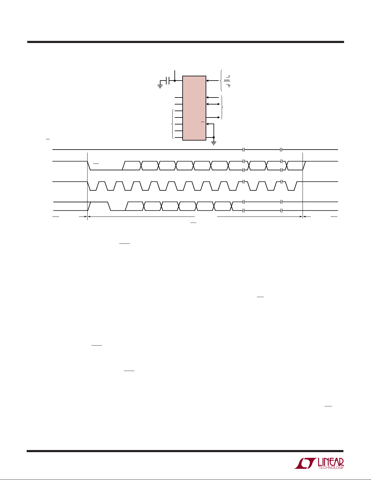
LTC2414/LTC2418
WUUU
APPLICATIO S I FOR ATIO
SDO
SCK
(INTERNAL)
2.7V TO 5.5V
1µF
919
V
F
CC
O
LTC2414/
LTC2418
11
REFERENCE
VOLTAGE
0.1V TO V
CC
ANALOG
INPUTS
CS
BIT 31
EOC
SDI
DON’T CARE DON’T CARE
(1) (0) EN SGL A2 A1 A0
BIT 27 BIT 26 BIT 25 BIT 24BIT 28BIT 29BIT 30
ODD/
SIGN
+
REF
12
–
REF
21
CH0
•
•
•
•
•
•
28
CH7
1
CH8
•
•
•
•
•
•
8
CH15
10
COM
20
SDI
18
SCK
17
SDO
CS
15
GND
DATA OUTPUT CONVERSIONCONVERSION
16
V
CC
= 50Hz REJECTION
= EXTERNAL OSCILLATOR
= 60Hz REJECTION
3-WIRE
SPI INTERFACE
Figure 10. Internal Serial Clock, CS = 0 Continuous Operation
BIT 6 BIT 0
LSBMSBSIG
PARITY
241418 F10
complete, SCK and SDO go LOW (EOC = 0) indicating the
conversion has finished and the device has entered the
low power sleep state. The part remains in the sleep state
a minimum amount of time (1/2 the internal SCK period)
then immediately begins outputting data. The data input/
output cycle begins on the first rising edge of SCK and
ends after the 32nd rising edge. The input data is then
shifted in via the SDI pin on the rising edge of SCK
(including the first rising edge) and the output data is
shifted out of the SDO pin on each falling edge of SCK.
The internally generated serial clock is output to the SCK
pin. This signal may be used to shift the conversion result
into external circuitry. EOC can be latched on the first
rising edge of SCK and the last bit of the conversion result
can be latched on the 32nd rising edge of SCK. After the
32nd rising edge, SDO goes HIGH (EOC = 1) indicating a
new conversion is in progress. SCK remains HIGH during
the conversion.
PRESERVING THE CONVERTER ACCURACY
The LTC2414/LTC2418 are designed to reduce as much as
possible the conversion result sensitivity to device
decoupling, PCB layout, antialiasing circuits, line fre-
quency perturbations and so on. Nevertheless, in order to
preserve the extreme accuracy capability of this part,
some simple precautions are desirable.
Digital Signal Levels
The LTC2414/LTC2418’s digital interface is easy to use.
Its digital inputs (SDI, F
, CS and SCK in External SCK mode
O
of operation) accept standard TTL/CMOS logic levels and
the internal hysteresis receivers can tolerate edge rates as
slow as 100µs. However, some considerations are required
to take advantage of the exceptional accuracy and low
supply current of this converter.
The digital output signals (SDO and SCK in Internal SCK
mode of operation) are less of a concern because they are
not generally active during the conversion state.
While a digital input signal is in the range 0.5V to
– 0.5V), the CMOS input receiver draws additional
(V
CC
current from the power supply. It should be noted that,
when any one of the digital input signals (SDI, F
, CS and
O
SCK in External SCK mode of operation) is within this
range, the power supply current may increase even if the
signal in question is at a valid logic level. For micropower
241418fa
24

WUUU
APPLICATIO S I FOR ATIO
LTC2414/LTC2418
operation, it is recommended to drive all digital input
signals to full CMOS levels [V
V
> (VCC – 0.4V)].
OH
< 0.4V and
IL
During the conversion period, the undershoot and/or
overshoot of a fast digital signal connected to the pins
may severely disturb the analog to digital conversion
process. Undershoot and overshoot can occur because of
the impedance mismatch at the converter pin when the
transition time of an external control signal is less than
twice the propagation delay from the driver to LTC2414/
LTC2418. For reference, on a regular FR-4 board, signal
propagation velocity is approximately 183ps/inch for
internal traces and 170ps/inch for surface traces. Thus, a
driver generating a control signal with a minimum transition time of 1ns must be connected to the converter pin
through a trace shorter than 2.5 inches. This problem
becomes particularly difficult when shared control lines
are used and multiple reflections may occur. The solution
is to carefully terminate all transmission lines close to
their characteristic impedance.
Parallel termination near the LTC2414/LTC2418 pin will
eliminate this problem but will increase the driver power
dissipation. A series resistor between 27Ω and 56Ω
placed near the driver or near the LTC2414/LTC2418 pin
will also eliminate this problem without additional power
dissipation. The actual resistor value depends upon the
trace impedance and connection topology.
An alternate solution is to reduce the edge rate of the
control signals. It should be noted that using very slow
edges will increase the converter power supply current
during the transition time. The differential input and reference architecture reduce substantially the converter’s
sensitivity to ground currents.
Particular attention must be given to the connection of the
FO signal when the LTC2414/LTC2418 are used with an
external conversion clock. This clock is active during the
conversion time and the normal mode rejection provided
by the internal digital filter is not very high at this frequency. A normal mode signal of this frequency at the
converter reference terminals may result into DC gain and
INL errors. A normal mode signal of this frequency at the
converter input terminals may result into a DC offset error.
Such perturbations may occur due to asymmetric capacitive coupling between the F
signal trace and the converter
O
input and/or reference connection traces. An immediate
solution is to maintain maximum possible separation
between the FO signal trace and the input/reference signals. When the F
signal is parallel terminated near the
O
converter, substantial AC current is flowing in the loop
formed by the F
connection trace, the termination and the
O
ground return path. Thus, perturbation signals may be
inductively coupled into the converter input and/or reference. In this situation, the user must reduce to a minimum
the loop area for the F
signal as well as the loop area for
O
the differential input and reference connections.
Driving the Input and Reference
The input and reference pins of the LTC2414/LTC2418
converters are directly connected to a network of sampling
capacitors. Depending upon the relation between the
differential input voltage and the differential reference
voltage, these capacitors are switching between these
four pins transferring small amounts of charge in the
process. A simplified equivalent circuit is shown in
Figure 11.
For a simple approximation, the source impedance R
S
driving an analog input pin (IN+, IN–, REF+ or REF–) can be
considered to form, together with R
and CEQ (see
SW
Figure 11), a first order passive network with a time
constant τ = (R
+ RSW) • CEQ. The converter is able to
S
sample the input signal with better than 1ppm accuracy if
the sampling period is at least 14 times greater than the
input circuit time constant τ. The sampling process on the
four input analog pins is quasi-independent so each time
constant should be considered by itself and, under worstcase circumstances, the errors may add.
When using the internal oscillator (F
= LOW or HIGH), the
O
LTC2414/LTC2418’s front-end switched-capacitor network is clocked at 76800Hz corresponding to a 13µs
sampling period. Thus, for settling errors of less than
1ppm, the driving source impedance should be chosen
such that τ ≤ 13µs/14 = 920ns. When an external oscillator
of frequency f
and, for a settling error of less than 1ppm, τ ≤ 0.14/f
is used, the sampling period is 2/f
EOSC
EOSC
EOSC
.
241418fa
25

LTC2414/LTC2418
WUUU
APPLICATIO S I FOR ATIO
Input Current
If complete settling occurs on the input, conversion results will be unaffected by the dynamic input current. An
incomplete settling of the input signal sampling process
may result in gain and offset errors, but it will not degrade
the INL performance of the converter. Figure 11 shows the
mathematical expressions for the average bias currents
+
flowing through the IN
and IN– pins as a result of the
sampling charge transfers when integrated over a substantial time period (longer than 64 internal clock cycles).
The effect of this input dynamic current can be analyzed
using the test circuit of Figure 12. The C
capacitor
PAR
includes the LTC2414/LTC2418 pin capacitance (5pF typical) plus the capacitance of the test fixture used to obtain
the results shown in Figures 13 and 14. A careful implementation can bring the total input capacitance (C
C
) closer to 5pF thus achieving better performance
PAR
IN
+
than the one predicted by Figures 13 and 14. For simplicity, two distinct situations can be considered.
For relatively small values of input capacitance (CIN <
0.01µF), the voltage on the sampling capacitor settles
almost completely and relatively large values for the
source impedance result in only small errors. Such values
for C
will deteriorate the converter offset and gain
IN
performance without significant benefits of signal filtering
and the user is advised to avoid them. Nevertheless, when
small values of CIN are unavoidably present as parasitics
of input multiplexers, wires, connectors or sensors, the
LTC2414/LTC2418 can maintain its exceptional accuracy
while operating with relative large values of source resistance as shown in Figures 13 and 14. These measured
results may be slightly different from the first order
approximation suggested earlier because they include the
effect of the actual second order input network together
with the nonlinear settling process of the input amplifiers.
For small CIN values, the settling on IN+ and IN– occurs
almost independently and there is little benefit in trying to
match the source impedance for the two pins.
Larger values of input capacitors (CIN > 0.01µF) may be
required in certain configurations for antialiasing or general input signal filtering. Such capacitors will average the
input sampling charge and the external source resistance
will see a quasi constant input differential impedance.
When F
= LOW (internal oscillator and 60Hz notch), the
O
V
CC
I
+
REF
V
+
REF
IIN+
VIN+
IIN–
VIN–
I
–
REF
V
–
REF
SWITCHING FREQUENCY
= 76800Hz INTERNAL OSCILLATOR (FO = LOW OR HIGH)
f
SW
= 0.5 • f
f
SW
I
LEAK
I
LEAK
V
CC
V
CC
I
LEAK
I
LEAK
V
CC
EXTERNAL OSCILLATOR
EOSC
I
LEAK
I
LEAK
I
LEAK
I
LEAK
RSW (TYP)
20k
RSW (TYP)
20k
RSW (TYP)
20k
RSW (TYP)
20k
Figure 11. LTC2414/LTC2418 Equivalent Analog Input Circuit
2414/18 F11
C
EQ
18pF
(TYP)
VV V
+ −
+
IIN
()
−
IIN
()
I REF
()
I REF
()
where
V REF REF
REF
V
REFCM
VININ
= −
IN
V
INCM
R M INTERNAL OSCILLATOR Hz Notch F LOW
==
EQ O
==
R M INTERNAL OSCILLATOR Hz Notch F HIGH
EQ O
=•
R f EXTERNAL OSCILLATOR
EQ EOSC
IN INCM REFCM
=
AVG
=
AVG
+
AVG
−
AVG
::
= −
⎛
=
⎜
⎝
+ −
⎛
IN IN
=
⎜
⎝
.
361 60
.
432 50
./
0 555 10
()
.
05
R
•
EQ
− + −
VV V
IN INCM REFCM
.
05
•
R
EQ
.
15
• − +
VV V
REF INCM REFCM
=
− • − +
15
=
+ −
+ −
REF REF
+ −
−
2
Ω
Ω
.
05
.
VV V
REF INCM REFCM
.
05
⎞
+
⎟
2
⎠
⎞
⎟
⎠
12
2
V
IN
•
R
EQ
•
R
EQ
−
•
VR
REF EQ
V
IN
+
VR
REF EQ
2
•
()
()
241418fa
26

R
SOURCE
(Ω)
1 10 100 1k 10k 100k
–FS ERROR (ppm OF V
REF
)
2414/18 F14
0
–10
–20
–30
–40
–50
VCC = 5V
REF
+
= 5V
REF
–
= GND
IN
+
= 1.25V
IN
–
= 3.75V
F
O
= GND
T
A
= 25°C
CIN = 0.01µF
CIN = 0.001µF
CIN = 100pF
CIN = 0pF
WUUU
APPLICATIO S I FOR ATIO
V
+ 0.5V
V
INCM
INCM
– 0.5V
IN
IN
R
SOURCE
R
SOURCE
LTC2414/LTC2418
+
IN
C
C
IN
C
IN
PAR
≅20pF
C
PAR
≅20pF
LTC2414/
LTC2418
–
IN
2414/18 F12
50
40
)
REF
30
VCC = 5V
20
REF
REF
IN
+FS ERROR (ppm OF V
IN
10
F
O
T
A
0
1 10 100 1k 10k 100k
Figure 13. +FS Error vs R
typical differential input resistance is 1.8MΩ which will
generate a gain error of approximately 0.28ppm for each
ohm of source resistance driving IN
HIGH (internal oscillator and 50Hz notch), the typical
differential input resistance is 2.16MΩ which will generate
a gain error of approximately 0.23ppm for each ohm of
source resistance driving IN
an external oscillator with a frequency f
conversion clock operation), the typical differential input
resistance is 0.28 • 10
source resistance driving IN
–6
• f
ppm gain error. The effect of the source
EOSC
IN
1.78 • 10
resistance on the two input pins is additive with respect to
this gain error. The typical +FS and –FS errors as a function
of the sum of the source resistance seen by IN
large values of C
In addition to this gain error, an offset error term may also
appear. The offset error is proportional with the mismatch
between the source impedance driving the two input pins
Figure 12. An RC Network at IN+ and IN
CIN = 0.01µF
CIN = 0.001µF
CIN = 100pF
CIN = 0pF
+
= 5V
–
= GND
+
= 3.75V
–
= 1.25V
= GND
= 25°C
R
(Ω)
SOURCE
at IN+ or IN– (Small CIN)
SOURCE
+
or IN–. When FO is driven by
12
/f
EOSC
+
or IN– will result in
2414/18 F13
+
or IN–. When FO =
(external
EOSC
Ω and each ohm of
+
and IN– for
are shown in Figures 15 and 16.
–
Figure 14. –FS Error vs R
+
IN
and IN– and with the difference between the input and
at IN+ or IN– (Small CIN)
SOURCE
reference common mode voltages. While the input drive
circuit nonzero source impedance combined with the
converter average input current will not degrade the INL
performance, indirect distortion may result from the modulation of the offset error by the common mode component
of the input signal. Thus, when using large C
capacitor
IN
values, it is advisable to carefully match the source impedance seen by the IN
+
and IN– pins. When FO = LOW (internal
oscillator and 60Hz notch), every 1Ω mismatch in source
impedance transforms a full-scale common mode input
signal into a differential mode input signal of 0.28ppm.
When F
= HIGH (internal oscillator and 50Hz notch), every
O
1Ω mismatch in source impedance transforms a full-scale
common mode input signal into a differential mode input
signal of 0.23ppm. When FO is driven by an external
oscillator with a frequency f
, every 1Ω mismatch in
EOSC
source impedance transforms a full-scale common
mode input signal into a differential mode input signal of
241418fa
27

LTC2414/LTC2418
WUUU
APPLICATIO S I FOR ATIO
300
VCC = 5V
+
= 5V
REF
–
REF
240
)
REF
180
120
+FS ERROR (ppm OF V
60
0
= GND
+
= 3.75V
IN
–
= 1.25V
IN
= GND
F
O
= 25°C
T
A
0
100 200 300 400 500 600 700 800 900 1000
Figure 15. +FS Error vs R
0
–60
)
REF
–120
VCC = 5V
–180
–FS ERROR (ppm OF V
–240
–300
+
= 5V
REF
–
= GND
REF
+
= 1.25V
IN
–
= 3.75V
IN
= GND
F
O
= 25°C
T
A
0
100 200 300 400 500 600 700 800 900 1000
Figure 16. –FS Error vs R
120
100
)
REF
–20
–40
–60
OFFSET ERROR (ppm OF V
–80
–100
–120
A
80
60
B
40
C
20
D
0
E
F
G
0
0.5 1 1.5 2 2.5 3 3.5 4 4.5 5
A: ∆RIN = +400Ω
= +200Ω
B: ∆R
IN
= +100Ω
C: ∆R
IN
= 0Ω
D: ∆R
IN
R
SOURCE
SOURCE
R
SOURCE
SOURCE
VCC = 5V
+
= 5V
REF
–
= GND
REF
+
= IN– = V
IN
FO = GND
= 25°C
T
A
R
SOURCEIN
= 10µF
C
IN
V
INCM
CIN = 1µF, 10µF
CIN = 0.1µF
CIN = 0.01µF
(Ω)
2414/18 F15
at IN+ or IN– (Large CIN)
CIN = 0.01µF
CIN = 0.1µF
CIN = 1µF, 10µF
(Ω)
2414/18 F16
at IN+ or IN– (Large CIN)
INCM
– = 500Ω
(V)
E: ∆RIN = –100Ω
= –200Ω
F: ∆R
IN
= –400Ω
G: ∆R
IN
2414/18 F17
Figure 17. Offset Error vs Common Mode Voltage
= IN+ = IN–) and Input Source Resistance Imbalance
(V
INCM
(∆RIN = R
SOURCEIN
+ – R
SOURCEIN
–) for Large CIN Values (CIN ≥ 1µF)
1.78 • 10–6 • f
ppm. Figure 17 shows the typical offset
EOSC
error due to input common mode voltage for various
values of source resistance imbalance between the IN
+
and IN– pins when large CIN values are used.
If possible, it is desirable to operate with the input signal
common mode voltage very close to the reference signal
common mode voltage as is the case in the ratiometric
measurement of a symmetric bridge. This configuration
eliminates the offset error caused by mismatched source
impedances.
The magnitude of the dynamic input current depends upon
the size of the very stable internal sampling capacitors and
upon the accuracy of the converter sampling clock. The
accuracy of the internal clock over the entire temperature
and power supply range is typical better than 0.5%. Such
a specification can also be easily achieved by an external
clock. When relatively stable resistors (50ppm/°C) are
used for the external source impedance seen by IN
–
, the expected drift of the dynamic current, offset and
IN
+
and
gain errors will be insignificant (about 1% of their respective values over the entire temperature and voltage range).
Even for the most stringent applications, a one-time
calibration operation may be sufficient.
In addition to the input sampling charge, the input ESD
protection diodes have a temperature dependent leakage
current. This current, nominally 1nA (±10nA max), results
in a small offset shift. A 100Ω source resistance will create
a 0.1µV typical and 1µV maximum offset voltage.
Reference Current
In a similar fashion, the LTC2414/LTC2418 samples the
differential reference pins REF+ and REF– transferring
small amount of charge to and from the external driving
circuits thus producing a dynamic reference current. This
current does not change the converter offset, but it may
degrade the gain and INL performance. The effect of this
current can be analyzed in the same two distinct situations.
For relatively small values of the external reference capacitors (C
< 0.01µF), the voltage on the sampling capacitor
REF
settles almost completely and relatively large values for
the source impedance result in only small errors. Such
241418fa
28

WUUU
R
SOURCE
(Ω)
1 10 100 1k 10k 100k
–FS ERROR (ppm OF V
REF
)
2414/18 F19
50
40
30
20
10
0
VCC = 5V
REF
+
= 5V
REF
–
= GND
IN
+
= 1.25V
IN
–
= 3.75V
F
O
= GND
T
A
= 25°C
C
REF
= 0.01µF
C
REF
= 0.001µF
C
REF
= 100pF
C
REF
= 0pF
APPLICATIO S I FOR ATIO
LTC2414/LTC2418
values for C
will deteriorate the converter offset and
REF
gain performance without significant benefits of reference
filtering and the user is advised to avoid them.
Larger values of reference capacitors (C
> 0.01µF) may
REF
be required as reference filters in certain configurations.
Such capacitors will average the reference sampling charge
and the external source resistance will see a quasi constant reference differential impedance. When F
= LOW
O
(internal oscillator and 60Hz notch), the typical differential
reference resistance is 1.3MΩ which will generate a gain
error of approximately 0.38ppm for each ohm of source
resistance driving REF
+
or REF–. When FO = HIGH (internal
oscillator and 50Hz notch), the typical differential reference resistance is 1.56MΩ which will generate a gain error
0
VCC = 5V
+
= 5V
REF
–
= GND
REF
–10
)
REF
–20
IN
IN
F
O
T
A
+
= 3.75V
–
= 1.25V
= GND
= 25°C
of approximately 0.32ppm for each ohm of source resis-
+
tance driving REF
external oscillator with a frequency f
or REF–. When FO is driven by an
(external conver-
EOSC
sion clock operation), the typical differential reference
resistance is 0.20 • 10
resistance driving REF
2.47 • 10
–6
• f
EOSC
12
/f
Ω and each ohm of source
EOSC
+
or REF– will result in
ppm gain error. The effect of the source
resistance on the two reference pins is additive with
respect to this gain error. The typical +FS and –FS errors
for various combinations of source resistance seen by the
+
and REF– pins and external capacitance C
REF
REF
connected to these pins are shown in Figures 18, 19, 20
and 21.
–30
+FS ERROR (ppm OF V
–40
–50
1 10 100 1k 10k 100k
Figure 18. +FS Error vs R
0
–90
)
REF
–180
Figure 20. +FS Error vs R
+FS ERROR (ppm OF V
VCC = 5V
–270
REF
REF
+
IN
–
IN
–360
–450
= GND
F
O
= 25°C
T
A
0
100 200 300 400 500 600 700 800 900 1000
C
REF
C
REF
C
REF
+
= 5V
–
= GND
= 3.75V
= 1.25V
= 0.01µF
= 0.001µF
= 100pF
C
= 0pF
REF
R
SOURCE
SOURCE
R
SOURCE
SOURCE
(Ω)
2414/18 F18
at REF+ or REF– (Small CIN)
C
= 0.01µF
REF
C
= 0.1µF
REF
C
= 1µF, 10µF
REF
(Ω)
2414/18 F20
at REF+ and REF– (Large C
Figure 19. –FS Error vs R
450
360
)
REF
270
180
–FS ERROR (ppm OF V
90
0
0
) Figure 21. –FS Error vs R
REF
at REF+ or REF– (Small CIN)
SOURCE
VCC = 5V
+
= 5V
REF
–
= GND
REF
+
= 1.25V
IN
–
= 3.75V
IN
= GND
F
O
= 25°C
T
A
100 200 300 400 500 600 700 800 900 1000
SOURCE
C
= 1µF, 10µF
REF
C
= 0.1µF
REF
C
= 0.01µF
REF
R
(Ω)
SOURCE
2414/18 F21
at REF+ and REF– (Large C
REF
241418fa
29
)

LTC2414/LTC2418
WUUU
APPLICATIO S I FOR ATIO
In addition to this gain error, the converter INL performance is degraded by the reference source impedance.
When F
100Ω of source resistance driving REF
into about 1.34ppm additional INL error. When F
= LOW (internal oscillator and 60Hz notch), every
O
+
or REF– translates
= HIGH
O
(internal oscillator and 50Hz notch), every 100Ω of source
+
resistance driving REF
1.1ppm additional INL error. When F
external oscillator with a frequency f
source resistance driving REF
about 8.73 • 10
or REF– translates into about
is driven by an
O
, every 100Ω of
EOSC
+
–6
• f
EOSC
or REF– translates into
ppm additional INL error.
Figure 22 shows the typical INL error due to the source
+
resistance driving the REF
or REF– pins when large C
REF
values are used. The effect of the source resistance on the
two reference pins is additive with respect to this INL error.
In general, matching of source impedance for the REF
+
and REF– pins does not help the gain or the INL error. The
user is thus advised to minimize the combined source
+
impedance driving the REF
and REF– pins rather than to
try to match it.
The magnitude of the dynamic reference current depends
upon the size of the very stable internal sampling capacitors and upon the accuracy of the converter sampling
clock. The accuracy of the internal clock over the entire
temperature and power supply range is typical better than
0.5%. Such a specification can also be easily achieved by
15
R
12
9
)
6
REF
3
0
–3
R
= 100Ω
INL (ppm OF V
–12
–15
Figure 22. INL vs Differential Input Voltage (VIN = IN+ – IN–)
and Reference Source Resistance (R
Large C
Values (C
REF
SOURCE
–6
–9
–0.5–0.4 –0.3– 0.2–0.1 0 0.1 0.2 0.3 0.4 0.5
VCC = 5V
REF+ = 5V
REF– = GND
= 0.5 • (IN+ + IN–) = 2.5V
V
INCM
≥ 1µF)
REF
SOURCE
R
SOURCE
V
INDIF/VREFDIF
= 1000Ω
= 500Ω
FO = GND
= 10µF
C
REF
= 25°C
T
A
2414/18 F22
at REF+ and REF– for
SOURCE
an external clock. When relatively stable resistors
(50ppm/°C) are used for the external source impedance
+
seen by REF
and REF–, the expected drift of the dynamic
current gain error will be insignificant (about 1% of its
value over the entire temperature and voltage range). Even
for the most stringent applications a onetime calibration
operation may be sufficient.
In addition to the reference sampling charge, the reference
pins ESD protection diodes have a temperature dependent
leakage current. This leakage current, nominally 1nA
(±10nA max), results in a small gain error. A 100Ω source
resistance will create a 0.05µV typical and 0.5µV maxi-
mum full-scale error.
Output Data Rate
When using its internal oscillator, the LTC2414/LTC2418
can produce up to 7.5 readings per second with a notch
frequency of 60Hz (F
second with a notch frequency of 50Hz (F
= LOW) and 6.25 readings per
O
= HIGH). The
O
actual output data rate will depend upon the length of the
sleep and data output phases which are controlled by the
user and which can be made insignificantly short. When
operated with an external conversion clock (F
connected
O
to an external oscillator), the LTC2414/LTC2418 output
data rate can be increased as desired up to that determined
by the maximum f
tion of the conversion phase is 20510/f
frequency of 2000kHz. The dura-
EOSC
. If f
EOSC
EOSC
=
153600Hz, the converter behaves as if the internal oscillator is used and the notch is set at 60Hz. There is no
significant difference in the LTC2414/LTC2418 performance between these two operation modes.
An increase in f
over the nominal 153600Hz will
EOSC
translate into a proportional increase in the maximum
output data rate. This substantial advantage is nevertheless accompanied by three potential effects, which must
be carefully considered.
First, a change in f
will result in a proportional change
EOSC
in the internal notch position and in a reduction of the
converter differential mode rejection at the power line
frequency. In many applications, the subsequent performance degradation can be substantially reduced by relying upon the LTC2414/LTC2418’s exceptional common
241418fa
30

WUUU
APPLICATIO S I FOR ATIO
LTC2414/LTC2418
mode rejection and by carefully eliminating common
mode to differential mode conversion sources in the input
circuit. The user should avoid single-ended input filters
and should maintain a very high degree of matching and
+
symmetry in the circuits driving the IN
and IN– pins.
Second, the increase in clock frequency will increase
proportionally the amount of sampling charge transferred
through the input and the reference pins. If large external
input and/or reference capacitors (C
IN
, C
) are used, the
REF
previous section provides formulae for evaluating the
effect of the source resistance upon the converter performance for any value of f
or reference capacitors (CIN, C
. If small external input and/
EOSC
) are used, the effect of
REF
the external source resistance upon the LTC2414/LTC2418
typical performance can be inferred from Figures 12, 13,
18 and 19 in which the horizontal axis is scaled by 153600/
f
.
EOSC
Third, an increase in the frequency of the external oscillator above 460800Hz (a more than 3× increase in the
output data rate) will start to decrease the effectiveness of
the internal autocalibration circuits. This will result in a
progressive degradation in the converter accuracy and
linearity. Typical measured performance curves for output
data rates up to 100 readings per second are shown in
Figures 23, 24, 25, 26, 27, 28, 29 and 30. In order to obtain
the highest possible level of accuracy from this converter
at output data rates above 20 readings per second, the
user is advised to maximize the power supply voltage used
and to limit the maximum ambient operating temperature.
In certain circumstances, a reduction of the differential
reference voltage may be beneficial.
Input Bandwidth
4
The combined effect of the internal Sinc
digital filter and
of the analog and digital autocalibration circuits determines the LTC2414/LTC2418 input bandwidth. When the
internal oscillator is used with the notch set at 60Hz
= LOW), the 3dB input bandwidth is 3.63Hz. When the
(F
O
internal oscillator is used with the notch set at 50Hz
(F
= HIGH), the 3dB input bandwidth is 3.02Hz. If an
O
external conversion clock generator of frequency f
EOSC
is
connected to the FO pin, the 3dB input bandwidth is 0.236
–6
• 10
• f
EOSC
.
200
160
)
120
ERROR
80
40
0
–40
VCC = 5V
–80
V
= 5V
REF
= 2.5V
V
IN
–120
OFFSET ERROR (ppm of V
–160
–200
= 2.5V
V
INCM
SDI = GND
= EXTERNAL OSCILLATOR
F
O
0 102030
OUTPUT DATA RATE (READINGS/SEC)
40
50
TA = 25°C
TA = 85°C
60 70 80 90 100
2414/18 F23
Figure 23. Offset Error vs Output Data Rate and Temperature
2000
0
)
REF
–2000
–4000
–6000
VCC = 5V
= 5V
V
–8000
+FS ERROR (ppm of V
–10000
–12000
REF
= 2.5V
V
IN
= 2.5V
V
INCM
SDI = GND
= EXTERNAL OSCILLATOR
F
O
0
20
10
OUTPUT DATA RATE (READINGS/SEC)
30 40
TA = 25°C
TA = 85°C
1009080706050
2414/18 F24
Figure 24. +FS Error vs Output Data Rate and Temperature
12000
VCC = 5V
= 5V
V
REF
10000
)
REF
–FS ERROR (ppm of V
–2000
= 2.5V
V
IN
= 2.5V
V
INCM
SDI = GND
8000
= EXTERNAL OSCILLATOR
F
O
6000
4000
2000
0
0
30 40
20
10
OUTPUT DATA RATE (READINGS/SEC)
TA = 85°C
TA = 25°C
1009080706050
2414/18 F25
Figure 25. –FS Error vs Output Data Rate and Temperature
241418fa
31

LTC2414/LTC2418
OUTPUT DATA RATE (READINGS/SEC)
200
150
100
50
0
–50
OFFSET ERROR (ppm of V
REF
)
2414/18 F28
0 102030
40
50
60 70 80 90 100
V
REF
= 5V
V
REF
= 2.5V
FO = EXTERNAL OSCILLATOR
V
CC
= 5V
REF
–
= GND
V
IN
= 0V
V
INCM
= 2.5V
SDI = GND
T
A
= 25°C
WUUU
APPLICATIO S I FOR ATIO
24
23
22
21
20
19
18
VCC = 5V
+
= 5V
REF
17
–
= GND
REF
16
RESOLUTION (BITS)
15
14
13
12
= 2.5V
V
INCM
= 0V
V
IN
SDI = GND
= EXTERNAL OSCILLATOR
F
O
RESOLUTION = LOG
0 102030405060708090100
OUTPUT DATA RATE (READINGS/SEC)
Figure 26. Resolution (Noise
TA = 85°C
2(VREF
TA = 25°C
/NOISE
RMS
)
RMS
2414/18 F26
≤ 1LSB)
vs Output Data Rate and Temperature
24
23
22
21
20
19
18
VCC = 5V
–
= GND
REF
17
16
RESOLUTION (BITS)
15
14
13
12
= 2.5V
V
INCM
= 0V
V
IN
SDI = GND
= EXTERNAL OSCILLATOR
F
O
= 25°C
T
A
RESOLUTION = LOG
0 102030405060708090100
OUTPUT DATA RATE (READINGS/SEC)
Figure 29. Resolution (Noise
V
= 5V
REF
V
= 2.5V
REF
2(VREF
/NOISE
RMS
≤ 1LSB) vs
RMS
)
2414/18 F29
Output Data Rate and Reference Voltage
22
RESOLUTION = LOG2(V
20
18
TA = 85°C
16
14
VCC = 5V
+
= 5V
REF
RESOLUTION (BITS)
–
= GND
REF
12
10
= 2.5V
V
INCM
–2.5V < V
SDI = GND
F
8
0 102030405060708090100
< 2.5V
IN
= EXTERNAL OSCILLATOR
O
OUTPUT DATA RATE (READINGS/SEC)
Figure 27. Resolution (INL
REF
TA = 25°C
/INL
RMS
)
MAX
2414/18 F27
≤ 1LSB)
vs Output Data Rate and Temperature
22
RESOLUTION =
20
18
16
V
= 2.5V
REF
14
TA = 25°C
= 5V
V
CC
RESOLUTION (BITS)
–
= GND
REF
12
10
= 0.5 • REF
V
INCM
–0.5V • V
REF
SDI = GND
= EXTERNAL OSCILLATOR
F
O
8
0 102030405060708090100
OUTPUT DATA RATE (READINGS/SEC)
LOG
+
< VIN < 0.5 • V
Figure 30. Resolution (INL
V
REF
2(VREF
= 5V
REF
MAX
/INL
)
MAX
2414/18 F30
≤ 1LSB) vs
Output Data Rate and Reference Voltage
Figure 28. Offset Error vs Output
Data Rate and Reference Voltage
0.0
–0.5
–1.0
–1.5
–2.0
–2.5
–3.0
–3.5
–4.0
–4.5
–5.0
INPUT SIGNAL ATTENUATION (dB)
–5.5
–6.0
0 0.5 1 1.5 2 2.5 3 3.5 4 4.5 5
DIFFERENTIAL INPUT SIGNAL FREQUENCY (Hz)
FO = HIGH FO = LOW
Figure 31. Input Signal Bandwidth
Using the Internal Oscillator
2414/18 F31
Due to the complex filtering and calibration algorithms
utilized, the converter input bandwidth is not modeled very
accurately by a first order filter with the pole located at the
3dB frequency. When the internal oscillator is used, the
shape of the LTC2414/LTC2418 input bandwidth is shown
in Figure 31 for FO = LOW and FO = HIGH. When an external
oscillator of frequency f
LTC2414/LTC2418 input bandwidth can be derived from
Figure 31, F
scaled by f
The conversion noise (1µV
be modeled by a white noise source connected to a noise
32
is used, the shape of the
EOSC
= LOW curve in which the horizontal axis is
O
/153600.
EOSC
typical for V
RMS
REF
= 5V) can
free converter. The noise spectral density is 78nV/√Hz for
an infinite bandwidth source and 107nV/√Hz for a single
0.5MHz pole source. From these numbers, it is clear that
particular attention must be given to the design of external
amplification circuits. Such circuits face the simultaneous
requirements of very low bandwidth (just a few Hz) in
order to reduce the output referred noise and relatively
high bandwidth (at least 500kHz) necessary to drive the
input switched-capacitor network. A possible solution is a
high gain, low bandwidth amplifier stage followed by a
high bandwidth unity-gain buffer.
241418fa

WUUU
FO = LOW OR
F
O
= EXTERNAL
OSCILLATOR,
f
EOSC
= 10 • f
S
DIFFERENTIAL INPUT SIGNAL FREQUENCY (Hz)
0f
S
INPUT NORMAL MODE REJECTION (dB)
2414/18 F34
0
–10
–20
–30
–40
–50
–60
–70
–80
–90
–100
–110
–120
2fS3fS4fS5fS6fS7fS8fS9fS10f
S
APPLICATIO S I FOR ATIO
When external amplifiers are driving the LTC2414/
LTC2418, the ADC input referred system noise calculation
can be simplified by Figure 32. The noise of an amplifier
driving the LTC2414/LTC2418 input pin can be modeled
as a band limited white noise source. Its bandwidth can be
approximated by the bandwidth of a single pole lowpass
filter with a corner frequency fi. The amplifier noise spectral density is n
selector, we can find on the y-axis the noise equivalent
bandwidth freq
width includes the band limiting effects of the ADC internal
calibration and filtering. The noise of the driving amplifier
referred to the converter input and including all these
effects can be calculated as N = n
noise (referred to the LTC2414/LTC2418 input) can now
be obtained by summing as square root of sum of squares
the three ADC input referred noise sources: the LTC2414/
LTC2418 internal noise (1µV), the noise of the IN
amplifier and the noise of the IN
If the F
f
EOSC
pin is driven by an external oscillator of frequency
O
, Figure 32 can still be used for noise calculation if the
x-axis is scaled by f
ratio f
EOSC
decrease, but in the same time the LTC2414/LTC2418
noise floor rises and the noise contribution of the driving
amplifiers lose significance.
Normal Mode Rejection and Antialiasing
One of the advantages delta-sigma ADCs offer over conventional ADCs is on-chip digital filtering. Combined with
a large oversampling ratio, the LTC2414/LTC2418 significantly simplify antialiasing filter requirements.
. From Figure 32, using fi as the x-axis
i
of the input driving amplifier. This band-
i
• √freqi. The total system
i
+
–
driving amplifier.
/153600. For large values of the
EOSC
driving
/153600, the Figure 32 plot accuracy begins to
LTC2414/LTC2418
100
10
1
INPUT REFERRED NOISE
EQUIVALENT BANDWIDTH (Hz)
0.1
0.1 1 10 100 1k 10k 100k 1M
INPUT NOISE SOURCE SINGLE POLE
EQUIVALENT BANDWIDTH (Hz)
Figure 32. Input Referred Noise Equivalent Bandwidth
of an Input Connected White Noise Source
0
FO = HIGH
–10
–20
–30
–40
–50
–60
–70
–80
–90
–100
INPUT NORMAL MODE REJECTION (dB)
–110
–120
0f
S2fS3fS4fS5fS6fS7fS8fS9fS
DIFFERENTIAL INPUT SIGNAL FREQUENCY (Hz)
Figure 33. Input Normal Mode Rejection,
Internal Oscillator and 50Hz Notch
FO = LOW
FO = HIGH
2414/18 F32
10fS11fS12f
2414/18 F33
S
The Sinc4 digital filter provides greater than 120dB normal
mode rejection at all frequencies except DC and integer
multiples of the modulator sampling frequency (f
LTC2414/LTC2418’s autocalibration circuits further simplify the antialiasing requirements by additional normal
mode signal filtering both in the analog and digital domain.
Independent of the operating mode, fS = 256 • fN = 2048
• f
OUTMAX
the maximum output data rate. In the internal oscillator
mode with a 50Hz notch setting, f
60Hz notch setting f
mode, f
where fN in the notch frequency and f
= f
S
EOSC
= 15360Hz. In the external oscillator
S
OUTMAX
= 12800Hz and with a
S
/10.
). The
S
is
Figure 34. Input Normal Mode Rejection, Internal
Oscillator and 60Hz Notch or External Oscillator
241418fa
33

LTC2414/LTC2418
WUUU
APPLICATIO S I FOR ATIO
The combined normal mode rejection performance is
shown in Figure 33 for the internal oscillator with 50Hz
notch setting (F
oscillator with 60Hz notch setting (F
= HIGH) and in Figure 34 for the internal
O
= LOW) and for the
O
external oscillator mode. The regions of low rejection
occurring at integer multiples of f
have a very narrow
S
bandwidth. Magnified details of the normal mode rejection
curves are shown in Figure 35 (rejection near DC) and
Figure 36 (rejection at fS = 256fN) where fN represents the
notch frequency. These curves have been derived for the
external oscillator mode but they can be used in all
operating modes by appropriately selecting the fN value.
The user can expect to achieve in practice this level of
performance using the internal oscillator as it is demonstrated by Figures 37 and 38. Typical measured values of
the normal mode rejection of the LTC2414/LTC2418
0
–10
–20
–30
–40
–50
–60
–70
–80
–90
–100
INPUT NORMAL MODE REJECTION (dB)
–110
–120
fN0 2fN3fN4fN5fN6fN7fN8f
INPUT SIGNAL FREQUENCY (Hz)
Figure 35. Input Normal Mode Rejection Figure 36. Input Normal Mode Rejection
N
2414/18 F35
operating with an internal oscillator and a 60Hz notch
setting are shown in Figure 37 superimposed over the
theoretical calculated curve. Similarly, typical measured
values of the normal mode rejection of the LTC2414/
LTC2418 operating with an internal oscillator and a 50Hz
notch setting are shown in Figure 38 superimposed over
the theoretical calculated curve.
As a result of these remarkable normal mode specifications, minimal (if any) antialias filtering is required in front
of the LTC2414/LTC2418. If passive RC components are
placed in front of the LTC2414/LTC2418, the input dynamic current should be considered (see Input Current
section). In cases where large effective RC time constants
are used, an external buffer amplifier may be required to
minimize the effects of dynamic input current.
0
–10
–20
–30
–40
–50
–60
–70
–80
–90
–100
INPUT NORMAL MODE REJECTION (dB)
–110
–120
250f
252fN254fN256fN258fN260fN262f
N
INPUT SIGNAL FREQUENCY (Hz)
N
2414/18 F36
0
–20
–40
–60
–80
NORMAL MODE REJECTION (dB)
–100
–120
0
15 30 45 60 75 90 105 120 135 150 165 180 195 210 225 240
MEASURED DATA
CALCULATED DATA
INPUT FREQUENCY (Hz)
VCC = 5V
+
= 5V
REF
–
REF
= GND
V
INCM
V
IN(P-P)
SDI = GND
= GND
F
O
T
= 25°C
A
Figure 37. Input Normal Mode Rejection vs Input Frequency
with Input Perturbation of 100% Full Scale (60Hz Notch)
34
= 2.5V
= 5V
2414/18 F37
0
–20
–40
–60
–80
NORMAL MODE REJECTION (dB)
–100
–120
0
12.5 25 37.5 50 62.5 75 87.5 100 112.5 125 137.5 150 162.5 175 187.5 200
INPUT FREQUENCY (Hz)
MEASURED DATA
CALCULATED DATA
VCC = 5V
+
= 5V
REF
–
REF
= GND
= 2.5V
V
INCM
V
IN(P-P)
SDI = GND
= 5V
F
O
T
= 25°C
A
= 5V
2414/18 F38
Figure 38. Input Normal Mode Rejection vs Input Frequency
with Input Perturbation of 100% Full Scale (50Hz Notch)
241418fa

WUUU
APPLICATIO S I FOR ATIO
LTC2414/LTC2418
Traditional high order delta-sigma modulators, while
providing very good linearity and resolution, suffer from
potential instabilities at large input signal levels. The proprietary architecture used for the LTC2414/LTC2418 third
order modulator resolves this problem and guarantees a
predictable stable behavior at input signal levels of up to
150% of full scale. In many industrial applications, it is not
uncommon to have to measure microvolt level signals
superimposed over volt level perturbations and LTC2414/
LTC2418 is eminently suited for such tasks. When the
perturbation is differential, the specification of interest is
the normal mode rejection for large input signal levels.
With a reference voltage V
= 5V, the LTC2414/LTC2418
REF
has a full-scale differential input range of 5V peak-to-peak.
0
–20
–40
–60
Figures 39 and 40 show measurement results for the
LTC2414/LTC2418 normal mode rejection ratio with a 7.5V
peak-to-peak (150% of full scale) input signal superimposed over the more traditional normal mode rejection
ratio results obtained with a 5V peak-to-peak (full scale)
input signal. In Figure 39, the LTC2414/LTC2418 uses the
internal oscillator with the notch set at 60Hz (F
= LOW)
O
and in Figure 40 it uses the internal oscillator with the
notch set at 50Hz (F
= HIGH). It is clear that the LTC2414/
O
LTC2418 rejection performance is maintained with no compromises in this extreme situation. When operating with
large input signal levels, the user must observe that such
signals do not violate the device absolute maximum
ratings.
V
= 5V
IN(P-P)
V
= 7.5V
IN(P-P)
(150% OF FULL SCALE)
VCC = 5V
+
REF
= 5V
–
REF
= GND
V
= 2.5V
INCM
SDI = GND
F
= GND
O
T
= 25°C
A
–80
NORMAL MODE REJECTION (dB)
–100
–120
0
15 30 45 60 75 90 105 120 135 150 165 180 195 210 225 240
INPUT FREQUENCY (Hz)
2414/18 F39
Figure 39. Measured Input Normal Mode Rejection vs Input Frequency with Input Perturbation of 150% Full Scale (60Hz Notch)
0
–20
–40
–60
–80
NORMAL MODE REJECTION (dB)
–100
–120
0
12.5 25 37.5 50 62.5 75 87.5 100 112.5 125 137.5 150 162.5 175 187.5 200
V
= 5V
IN(P-P)
V
= 7.5V
IN(P-P)
(150% OF FULL SCALE)
INPUT FREQUENCY (Hz)
VCC = 5V
+
REF
= 5V
–
REF
= GND
V
= 2.5V
INCM
SDI = GND
F
= 5V
O
T
= 25°C
A
2414/18 F40
Figure 40. Measured Input Normal Mode Rejection vs Input Frequency with Input Perturbation of 150% Full Scale (50Hz Notch)
241418fa
35

LTC2414/LTC2418
WUUU
APPLICATIO S I FOR ATIO
BRIDGE APPLICATIONS
Typical strain gauge based bridges deliver only 2mV/Volt
of excitation. As the maximum reference voltage of the
LTC2414/LTC2418 is 5V, remote sensing of applied excitation without additional circuitry requires that excitation
be limited to 5V. This gives only 10mV full scale input
signal, which can be resolved to 1 part in 10000 without
averaging. For many solid state sensors, this is still better
than the sensor. Averaging 64 samples however reduces
the noise level by a factor of eight, bringing the resolving
power to 1 part in 80000, comparable to better weighing
systems. Hysteresis and creep effects in the load cells are
typically much greater than this. Most applications that
require strain measurements to this level of accuracy are
measuring slowly changing phenomena, hence the time
required to average a large number of readings is usually
not an issue. For those systems that require accurate
measurement of a small incremental change on a significant tare weight, the lack of history effects in the LTC2400
family is of great benefit.
For those applications that cannot be fulfilled by the
LTC2414/LTC2418 alone, compensating for error in external amplification can be done effectively due to the “no
latency” feature of the LTC2414/LTC2418. No latency
operation allows samples of the amplifier offset and gain
to be interleaved with weighing measurements. The use of
correlated double sampling allows suppression of 1/f
noise, offset and thermocouple effects within the bridge.
Correlated double sampling involves alternating the polarity of excitation and dealing with the reversal of input
polarity mathematically. Alternatively, bridge excitation
can be increased to as much as ±10V, if one of several
precision attenuation techniques is used to produce a
precision divide operation on the reference signal. Another option is the use of a reference within the 5V input
range of the LTC2414/LTC2418 and developing excitation
via fixed gain, or LTC1043 based voltage multiplication,
along with remote feedback in the excitation amplifiers, as
shown in Figures 46 and 47.
Figure 41 shows an example of a simple bridge connection. Note that it is suitable for any bridge application
where measurement speed is not of the utmost importance. For many applications where large vessels are
weighed, the average weight over an extended period of
time is of concern and short term weight is not readily
determined due to movement of contents, or mechanical
resonance. Often, large weighing applications involve load
cells located at each load bearing point, the output of
which can be summed passively prior to the signal processing circuitry, actively with amplification prior to the
ADC, or can be digitized via multiple ADC channels and
summed mathematically. The mathematical summation
of the output of multiple LTC2414/LTC2418’s provides the
benefit of a root square reduction in noise. The low power
consumption of the LTC2414/LTC2418 makes it attractive
for multidrop communication schemes where the ADC is
located within the load-cell housing.
LT1019
SDI
SCK
+
20
18
17
16
CS
19
F
O
2414/18 F41
R1
BRIDGE
R2
R1 AND R2 CAN BE USED TO INCREASE TOLERABLE AC COMPONENT ON REF SIGNALS
0.1µF 0.1µF10µF
11
12350Ω
21
22
Figure 41. Simple Bridge Connection
REF
REF
CH0
LTC2414/
LTC2418
CH1
+
–
V
CC
GND
9
SDO
15
A direct connection to a load cell is perhaps best incorporated into the load-cell body, as minimizing the distance to
the sensor largely eliminates the need for protection
devices, RFI suppression and wiring. The LTC2414/
LTC2418 exhibits extremely low temperature dependent
drift. As a result, exposure to external ambient temperature ranges does not compromise performance. The incorporation of any amplification considerably complicates thermal stability, as input offset voltages and currents, temperature coefficient of gain settling resistors all
become factors.
241418fa
36

WUUU
APPLICATIO S I FOR ATIO
LTC2414/LTC2418
The circuit in Figure 42 shows an example of a simple
amplification scheme. This example produces a differential output with a common mode voltage of 2.5V, as
determined by the bridge. The use of a true three amplifier
instrumentation amplifier is not necessary, as the LTC2414/
LTC2418 has common mode rejection far beyond that of
most amplifiers. The LTC1051 is a dual autozero amplifier
that can be used to produce a gain of 15 before its input
referred noise dominates the LTC2414/LTC2418 noise.
This example shows a gain of 34, that is determined by a
feedback network built using a resistor array containing 8
individual resistors. The resistors are organized to optimize temperature tracking in the presence of thermal
gradients. The second LTC1051 buffers the low noise
input stage from the transient load steps produced during
conversion.
The gain stability and accuracy of this approach is very
good, due to a statistical improvement in resistor matching. A gain of 34 may seem low, when compared to
common practice in earlier generations of load-cell interfaces, however the accuracy of the LTC2414/LTC2418
changes the rationale. Achieving high gain accuracy and
linearity at higher gains may prove difficult, while providing little benefit in terms of noise reduction.
At a gain of 100, the gain error that could result from
typical open-loop gain of 160dB is –1ppm, however,
worst-case is at the minimum gain of 116dB, giving a gain
error of –158ppm. Worst-case gain error at a gain of 34,
is –54ppm. The use of the LTC1051A reduces the worstcase gain error to –33ppm. The advantage of gain higher
than 34, then becomes dubious, as the input referred
noise sees little improvement and gain accuracy is potentially compromised.
Note that this 4-amplifier topology has advantages over
the typical integrated 3-amplifier instrumentation amplifier in that it does not have the high noise level common in
the output stage that usually dominates when and instrumentation amplifier is used at low gain. If this amplifier is
used at a gain of 10, the gain error is only 10ppm and input
referred noise is reduced to 0.1µV
. The buffer stages
RMS
can also be configured to provide gain of up to 50 with high
gain stability and linearity.
350Ω
BRIDGE
5V
3
+
U1A
2
–
1
RN1
16
RN1 = 5k × 8 RESISTOR ARRAY
U1A, U1B, U2A, U2B = 1/2 LTC1051
15
611
2
6
–
U1B
5
+
0.1µF
8
1
4
14
710
3
7
4
89
13
512
0.1µF
5V
8
2
–
U2A
3
+
6
–
U2B
5
+
1
4
7
Figure 42. Using Autozero Amplifiers to Reduce Input Referred Noise
11
12
21
22
2414/18 F42
REF
REF
CH0
LTC2414/
CH1
V
CC
+
–
LTC2418
GND
15
2
SDI
SCK
SD0
5V
0.1µF
CS
F
O
REF
20
18
17
16
19
241418fa
37

LTC2414/LTC2418
WUUU
APPLICATIO S I FOR ATIO
Figure 43 shows an example of a single amplifier used to
produce single-ended gain. This topology is best used in
applications where the gain setting resistor can be made
to match the temperature coefficient of the strain gauges.
If the bridge is composed of precision resistors, with only
one or two variable elements, the reference arm of the
bridge can be made to act in conjunction with the feedback
resistor to determine the gain. If the feedback resistor is
incorporated into the design of the load cell, using resistors which match the temperature coefficient of the loadcell elements, good results can be achieved without the
need for resistors with a high degree of absolute accuracy.
The common mode voltage in this case, is again a function
of the bridge output. Differential gain as used with a 350Ω
bridge is A
= (R1+ R2)/(R1+175Ω). Common mode gain
V
is half the differential gain. The maximum differential
signal that can be used is 1/4 V
, as opposed to 1/2 V
REF
REF
in the 2-amplifier topology above.
Remote Half Bridge Interface
As opposed to full bridge applications, typical half bridge
applications must contend with nonlinearity in the bridge
output, as signal swing is often much greater. Applications
include RTD’s, thermistors and other resistive elements
that undergo significant changes over their span. For
single variable element bridges, the nonlinearity of the half
bridge output can be eliminated completely; if the reference arm of the bridge is used as the reference to the ADC,
as shown in Figure 44. The LTC2414/LTC2418 can accept
inputs up to 1/2 V
. Hence, the reference resistor R1
REF
must be at least 2x the highest value of the variable
resistor.
In the case of 100Ω platinum RTD’s, this would suggest a
value of 800Ω for R1. Such a low value for R1 is not
advisable due to self-heating effects. A value of 25.5k is
shown for R1, reducing self-heating effects to acceptable
levels for most sensors.
350Ω
BRIDGE
+
5V
0.1µV
7
3
1µF
AV = 9.95 =
+
LTC1050S8
2
–
4
R1
4.99k
R1 + R2
()
R1 + 175Ω
R2
46.4k
175Ω
6
+
1µF
Figure 43. Bridge Amplification Using a Single Amplifier
20k
20k
10µF
+
–
V
GND
5V
0.1µF
9
CC
15
2410 F49
R1
25.5k
0.1%
PLATINUM
100Ω
RTD
11
12
21
22
+
11
REF
12
REF
21
CH0
LTC2414/
LTC2418
22
CH1
V
S
2.7V TO 5.5V
9
V
CC
+
REF
LTC2414/
LTC2418
–
REF
CH0
CH1
GND
15
2410 F50
Figure 44. Remote Half Bridge Interface
38
241418fa

WUUU
APPLICATIO S I FOR ATIO
LTC2414/LTC2418
The basic circuit shown in Figure 44 shows connections
for a full 4-wire connection to the sensor, which may be
located remotely. The differential input connections will
reject induced or coupled 60Hz interference, however, the
reference inputs do not have the same rejection. If 60Hz or
other noise is present on the reference input, a low pass
filter is recommended as shown in Figure 45. Note that you
cannot place a large capacitor directly at the junction of R1
and R2, as it will store charge from the sampling process.
A better approach is to produce a low pass filter decoupled
from the input lines with a high value resistor (R3).
The use of a third resistor in the half bridge, between the
variable and fixed elements gives essentially the same
result as the two resistor version, but has a few benefits.
If, for example, a 25k reference resistor is used to set the
excitation current with a 100Ω RTD, the negative reference input is sampling the same external node as the
positive input and may result in errors if used with a long
cable. For short cable applications, the errors may be
acceptably low. If instead the single 25k resistor is replaced with a 10k 5% and a 10k 0.1% reference resistor,
the noise level introduced at the reference, at least at
higher frequencies, will be reduced. A filter can be introduced into the network, in the form of one or more
capacitors, or ferrite beads, as long as the sampling pulses
are not translated into an error. The reference voltage is
also reduced, but this is not undesirable, as it will decrease
the value of the LSB, although, not the input referred noise
level.
The circuit shown in Figure 45 shows a more rigorous
example of Figure 44, with increased noise suppression
and more protection for remote applications.
Figure 46 shows an example of gain in the excitation circuit
and remote feedback from the bridge. The LTC1043’s
provide voltage multiplication, providing ±10V from a 5V
reference with only 1ppm error. The amplifiers are used at
unity gain and introduce very little error due to gain error
or due to offset voltages. A 1µV/°C offset voltage drift
translates into 0.05ppm/°C gain error. Simpler alternatives, with the amplifiers providing gain using resistor
arrays for feedback, can produce results that are similar to
bridge sensing schemes via attenuators. Note that the
amplifiers must have high open-loop gain or gain error will
be a source of error. The fact that input offset voltage has
relatively little effect on overall error may lead one to use
low performance amplifiers for this application. Note that
the gain of a device such as an LF156, (25V/mV over
temperature) will produce a worst-case error of –180ppm
at a noise gain of 3, such as would be encountered in an
inverting gain of 2, to produce –10V from a 5V reference.
R2
10k
0.1%
R1
10k, 5%
PLATINUM
100Ω
RTD
Figure 45. Remote Half Bridge Sensing with Noise Suppression on Reference
R3
10k
5%
1µF
5V
+
LTC1050
–
560Ω
10k
10k
11
+
REF
12
–
REF
LTC2414/
LTC2418
21
CH0
22
CH1
5V
V
GND
9
CC
15
2410 F51
241418fa
39

LTC2414/LTC2418
WUUU
APPLICATIO S I FOR ATIO
The error associated with the 10V excitation would be
–80ppm. Hence, overall reference error could be as high
as 130ppm, the average of the two.
Figure 47 shows a similar scheme to provide excitation
using resistor arrays to produce precise gain. The circuit
15V15V
350Ω
BRIDGE
Q1
2N3904
33Ω
10V
–15V
–10V
33Ω
Q2
2N3906
20Ω
20Ω
7
38
LTC1150
4
–15V
15V
7
LTC1150
4
–15V
+
1µF
2
–
3
+
2
–
6
0.1µF
1k
6
200Ω
10V 5V
is configured to provide 10V and –5V excitation to the
bridge, producing a common mode voltage at the input to
the LTC2414/LTC2418 of 2.5V, maximizing the AC input
range for applications where induced 60Hz could reach
amplitudes up to 2V
15V
14
U1
LTC1043
11
12
U2
LTC1043
5
15
4
7
*
13
17
6
2
*
3
18
.
RMS
LT1236-5
+
47µF 0.1µF
+
10µF
0.1µF
11
12
21
22
LTC2414/
LTC2418
REF
REF
CH0
CH1
+
–
V
GND
9
CC
15
10V
5V
40
0.1µF
1k
5V
4
11
*
12
17
–10V
1µF
FILM
–10V
200Ω
8
14
U2
LTC1043
*FLYING CAPACITORS ARE
1µF FILM (MKP OR EQUIVALENT)
SEE LTC1043 DATA SHEET FOR
DETAILS ON UNUSED HALF OF U1
7
13
Figure 46. LTC1043 Provides Precise 4X Reference for Excitation Voltages
2410 F52
241418fa

WUUU
APPLICATIO S I FOR ATIO
15V
–5V
20Ω
RN1
10k
RN1
10k
350Ω BRIDGE
TWO ELEMENTS
VARYING
Q1
2N3904
22Ω
10V
LTC2414/LTC2418
3
+
C1
0.1µF
1/2
LT1112
2
–
3
RN1
10k
4
1
21
65
5V
LT1236-5
+
C3
47µF
9
V
CC
LTC2414/
LTC2418
11
+
REF
12
–
REF
21
CH0
22
8
RN1
10k
7
CH1
GND
15
C1
0.1µF
5V
15V
7
C2
0.1µF
8
LT1112
4
–15V
33Ω
×2
Q2, Q3
2N3906
20Ω
×2
–15V
Figure 47. Use Resistor Arrays to Provide Precise Matching in Excitation Amplifier
MULTIPLE CHANNEL USAGE
The LTC2414/LTC2418 have up to sixteen input channels
and this feature provides a very flexible and efficient
solution in applications where more than one variable
need to be measured.
Measurements of a Ladder of Sensors
In industrial process, it is likely that a large group of real
world phenomena need to be monitored where the speed
is not critical. One example is the cracking towers in
petroleum refineries where a group of temperature measurements need to be taken and related. This is done by
passing an excitation current through a ladder of RTDs.
The configuration using a single LTC2418 to monitor up to
eight RTDs in differential mode is shown in Figure 48. A
high accuracy R1 is used to set the excitation current and
the reference voltage. A larger value of 25k is selected to
RN1 IS CADDOCK T914 10K-010-02
2410 F53
1/2
6
–
5
+
reduce the self-heating effects. R1 can also be broken into
two resistors, one 25k to set the excitation current and the
other a high accuracy 1k resistor to set the reference
voltage, assuming 100Ω platinum RTDs. This results in a
reduced reference voltage and a reduced common mode
difference between the reference and the input signal,
which improves the conversion linearity and reduces total
error.
Each input should be taken close to the related RTD to
minimize the error caused by parasitic wire resistance.
The interference on a signal transmission line from RTD to
the LTC2418 is rejected due to the excellent common
mode rejection and the digital LPF included in the LTC2418.
It should be noted that the input source resistance of CHO
can have a maximum value of 800Ω • 8 = 6.4k, so the
parasitic capacitance and resistance of the connection
wires need to be minimized in order not to degrade the
converter performance.
241418fa
41

LTC2414/LTC2418
WUUU
APPLICATIO S I FOR ATIO
5V
0.1µF
+
0.1%
PT1
100Ω
RTD
PT2
100Ω
RTD
PT8
100Ω
RTD
25k
10µF
R1
•
•
•
9
11
12
21
22
23
24
V
CC
+
REF
–
REF
LTC2418
CH0
15
SDI
SCK
SDO
20
18
4-WIRE
17
16
CS
19
F
O
2418 F48
SPI
CH1
CH2
CH3
•
•
•
7
CH14
8
CH15
GND
Figure 48. Measurement of a Ladder of Sensors Using
Differential Mode
Figure 49 shows the 4-wire SPI connection between the
LTC2414/LTC2418 and a PIC16F84 microcontroller. The
sample program for CC5X compiler in Figure 50 can be
used to program the PIC16F84 to control the LTC2414/
LTC2418. It uses PORT B to interface with the device.
The program begins by declaring variables and allocating
four memory locations to store the 32-bit conversion
result. In execution, it first initiates the PORT B to the
proper SPI configuration and prepares channel address.
The LTC2414/LTC2418 is activated by setting the CS low.
Then the microcontroller waits until a logic LOW is detected on the data line, signifying end-of-conversion. After
a LOW is detected, a subroutine is called to exchange data
between the LTC2414/LTC2418 and the microcontroller.
The main loop ends by setting CS high, ending the data
output state.
The performance of the LTC2414/LTC2418 can be verified
using the demonstration board DC434A, see Figure 51 for
the schematic. This circuit uses the computer’s serial port
to generate power and the SPI digital signals necessary for
starting a conversion and reading the result. It includes a
Multichannel Bridge Digitizer and Digital Cold
Junction Compensation
The bridge application as shown in Figures 41, 42, and 43
can be expanded to multiple bridge transducers. Figure 54
shows the expansion for simple bridge measurement.
Also included is the temperature measurement.
In Figure 54, CH0 to CH13 are configured as differential to
measure up to seven bridge transducers using the LTC2418.
CH14 and CH15 are configured as single-ended. CH14
measures the thermocouple while CH15 measures the
output of the cold junction sensor (diode, thermistor,
etc.). The measured cold junction sensor output is then
used to compensate the thermocouple output to find the
absolute temperature. The final temperature value may
then be used to compensate the temperature effects of the
bridge transducers.
Sample Driver for LTC2414/LTC2418 SPI Interface
The LTC2414/LTC2418 have a simple 4-wire serial interface and it is easy to program microprocessors and
microcontrollers to control the device.
PIC16F84
LTC2414/
LTC2418
SCK
SDI
SDO
18
20
17
16
CS
8
RB2
9
RB3
10
RB4
11
RB5
2414/18 F49
Figure 49. Connecting the LTC2414/LTC2418 to
a PIC16F84 MCU Using the SPI Serial Interface
LabVIEWTM application software program (see Figure 52)
which graphically captures the conversion results. It can
be used to determine noise performance, stability and with
an external source linearity. As exemplified in the schematic, the LTC2414/LTC2418 is extremely easy to use.
This demonstration board and associated software is
available by contacting Linear Technology.
241418fa
42

WUUU
APPLICATIO S I FOR ATIO
// LTC2418 PIC16F84 Interface Example
// Written for CC5X Compiler
// Processor is PIC16F84 running at 10 MHz
#include <16f84.h>
#include <int16cxx.h>
#pragma origin = 0x4
#pragma config |= 0x3fff, WDTE=off,FOSC=HS
// global pin definitions:
#pragma bit rx_pin @ PORTB.0 //input
#pragma bit tx_pin @ PORTB.1 //output
#pragma bit sck @ PORTB.2 //output
#pragma bit sdi @ PORTB.3 //output
#pragma bit sdo @ PORTB.4 //input
#pragma bit cs_bar @ PORTB.5 //output
// Global Variables
uns8 result_3; // Conversion result MS byte
uns8 result_2; // ..
uns8 result_1; // ..
uns8 result_0; // Conversion result LS byte
void shiftbidir(char nextch); // function prototype
void main( void)
{
INTCON=0b00000000; // no interrupts
TRISA=0b00000000; // all PORTA pins outputs
TRISB=0b00010001; // according to definitions above
LTC2414/LTC2418
char channel; // next channel to send
while(1)
{
/* channel bit fields are 7:6, 10 always; 5, EN; 4, SGL; 3, ODD/SIGN; 2:0, ADDR */
channel = 0b10101000; // CH0,1 DIFF.
cs_bar=0; // activate ADC
while(sdo==1) // test for end of conversion
{
// wait if conversion is not complete
}
shiftbidir(channel); // read ADC, send next channel
cs_bar = 1; // deactivate ADC
/* At this point global variables result 3,2,1 contain the 24 bit conversion result. Variable result3
contains the corresponding channel information in the following fields:
bits 7:6, 00 always, 5, EN; 4, SGL; 3, ODD/SIGN; 2:0, ADDR */
} // end of loop
} // end of main
Figure 50. Sample Program in CC5X for PIC16F84
241418fa
43

LTC2414/LTC2418
WUUU
APPLICATIO S I FOR ATIO
////////// Bidirectional Shift Routine for ADC //////////
void shiftbidir(char nextch)
{
int i;
for(i=0;i<2;i++) // send config bits 7:6,
// ignore EOC/ and DMY bits
{
sdi=nextch.7; // put data on pin
nextch = rl(nextch); // get next config bit ready
sck=1; // clock high
sck=0; // clock low
}
for(i=0;i<8;i++) // send config, read byte 3
{
sdi=nextch.7; // put data on pin
nextch = rl(nextch); // get next config bit ready
result_3 = rl(result_3);// get ready to load lsb
result_3.0 = sdo; // load lsb
sck=1; // clock high
sck=0; // clock low
}
for(i=0;i<8;i++) // read byte 2
{
result_2 = rl(result_2);// get ready to load lsb
result_2.0 = sdo; // load lsb
sck=1; // clock high
sck=0; // clock low
}
for(i=0;i<8;i++) // read byte 1
{
result_1 = rl(result_1);// get ready to load lsb
result_1.0 = sdo; // load lsb
sck=1; // clock high
sck=0; // clock low
}
result_0=0; // ensure bits 7:6 are zero
for(i=0;i<6;i++) // read byte 0
{
result_0 = rl(result_0);// get ready to load lsb
result_0.0 = sdo; // load lsb
sck=1; // clock high
sck=0; // clock low
}
}
44
Figure 50. Sample Program in CC5X for PIC16F84 (cont)
241418fa

WUUU
APPLICATIO S I FOR ATIO
LTC2414/LTC2418
VEX
REF
REF
GND
BANANA
JACK
J1
J2
+
J3
–
J4
V
CC
1
1
V
1
GND NC
11
13
15
17
19
21
23
25
27
29
31
33
35
37
39
GND
JP1
JMPR
CC
2
2
1
3
5
7
9
2
2.5V
NC
3
JMPR
3
P2
CON40A
3
JP3
JP5
JMPR
JP6
JMPR
LT1460ACN8-2.5
V
R2
3Ω
V
GND
OUT
GND
3
E3
CC
E4
+ +
C1
10µF
35V
2.5V 5V
1
2
2
4
6
8
10
12
14
16
18
20
22
24
26
28
30
32
34
36
38
40
U1
C6
0.1µF
V
IN
+
11
12
21
22
23
24
25
26
27
28
1
2
3
4
5
6
7
8
REMOVE TO
DISCONNECT
V
C2
22µF
25V
V
CC
C5
10µF
35V
9
V
CC
U5
LTC2418CGN
REF+
REF–
SCK
CH0
SDO
CH1
CH2
CH3
CH4
CH5
CH6
CH7
CH8
CH9
CH10
CH11
CH12
CH13
CH14
CH15
GND
COM
10
AND
CC
5V REF
1
JP4
JMPR
F
O
CS
SDI
NC
NC
50Hz/60Hz
2
19
18
17
16
20
13
14
15
V
CC
1
V
CC
2
C3
NC
JP2
JMPR
V
CC
3
+
10µF
35V
3
74HC14
74HC14
10
11
12
13
14
3
4
5
6
2
15
1
LT1236ACN8-5
V
OUT
U3E
U3B
74HC14
SER
A
B
U4
C
74HC165
D
E
F
G
H
CLK
INH
SH/LD
U3C
GND
U2
GND
V
CC
QH
QH
V
IN
+
C4
100µF
16V
U3F
74HC14
U3A
74HC14
R7
V
CC
22k
16
R8
51k
9
7
8
R1
10Ω
U3D
74HC14
D1
BAV74LT1
R3
51k
R4
51k
R6
3k
E1
E2
R5
49.9Ω
Q1
MMBT3904LT1
V
CC
C7
0.1µF
BYPASS
CAPACITOR
FOR U3 AND U4
V
V
EXT
GND
1
6
2
7
3
8
4
9
5
CC
2414/18 F51
DB9
C8
0.1µF
P1
Figure 51. Demo Board Schematic
241418fa
45

LTC2414/LTC2418
WUUU
APPLICATIO S I FOR ATIO
Top Silkscreen
Figure 52. LTC2418 Demo Program Display
Top Layer
Bottom Layer
46
Figure 53. PCB Layout and Film
241418fa

PACKAGE DESCRIPTIO
LTC2414/LTC2418
U
GN Package
28-Lead Plastic SSOP (Narrow .150 Inch)
(Reference LTC DWG # 05-08-1641)
0.015 ± 0.004
(0.38
0.0075 – 0.0098
(0.191 – 0.249)
0.016 – 0.050
(0.406 – 1.270)
* DIMENSION DOES NOT INCLUDE MOLD FLASH. MOLD FLASH
SHALL NOT EXCEED 0.006" (0.152mm) PER SIDE
** DIMENSION DOES NOT INCLUDE INTERLEAD FLASH. INTERLEAD
FLASH SHALL NOT EXCEED 0.010" (0.254mm) PER SIDE
0° – 8° TYP
± 0.10)
× 45°
0.229 – 0.244
(5.817 – 6.198)
0.053 – 0.069
(1.351 – 1.748)
0.008 – 0.012
(0.203 – 0.305)
12
0.386 – 0.393*
(9.804 – 9.982)
202122232425262728
19
18
16
17
15
5
4
3
678 9 10 11 12
0.0250
(0.635)
BSC
13 14
0.033
(0.838)
REF
0.150 – 0.157**
(3.810 – 3.988)
0.004 – 0.009
(0.102 – 0.249)
GN28 (SSOP) 1098
Information furnished by Linear Technology Corporation is believed to be accurate and reliable.
However, no responsibility is assumed for its use. Linear Technology Corporation makes no representation that the interconnection of its circuits as described herein will not infringe on existing patent rights.
241418fa
47

LTC2414/LTC2418
TYPICAL APPLICATIO
THERMISTOR
U
THERMOCOUPLE
5V
0.1µF
+
10µF
9
V
V
11
12
•••
21
22
REF
REF
CH0
CH1
CC
CC
+
LTC2418
–
LTC2418
SDI
20
15
SCK
SDO
18
17
16
CS
19
F
O
2418 F54
23
CH2
24
CH3
•
•
•
•
•
•
7
CH14
8
CH15
10
COM
GND
GND
Figure 54. Multichannel Bridge Digitizer and Digital Cold Junction Compensation
RELATED PARTS
PART NUMBER DESCRIPTION COMMENTS
LT1019 Precision Bandgap Reference, 2.5V, 5V 3ppm/°C Drift, 0.05% Max Initial Accuracy
LT1025 Micropower Thermocouple Cold Junction Compensator 80µA Supply Current, 0.5°C Initial Accuracy
LTC1050 Precision Chopper Stabilized Op Amp No External Components 5µV Offset, 1.6µV
LT1236A-5 Precision Bandgap Reference, 5V 0.05% Max Initial Accuracy, 5ppm/°C Drift
LT1460 Micropower Series Reference 0.075% Max Initial Accuracy, 10ppm/°C Max Drift
LTC2400 24-Bit, No Latency ∆Σ ADC in SO-8 0.3ppm Noise, 4ppm INL, 10ppm Total Unadjusted Error, 200µA
LTC2401/LTC2402 1-/2-Channel, 24-Bit, No Latency ∆Σ ADC in MSOP 0.6ppm Noise, 4ppm INL, 10ppm Total Unadjusted Error, 200µA
LTC2404/LTC2408 4-/8-Channel, 24-Bit, No Latency ∆Σ ADC 0.3ppm Noise, 4ppm INL, 10ppm Total Unadjusted Error, 200µA
LTC2410 24-Bit, Fully Differential, No Latency ∆Σ ADC 0.16ppm Noise, 2ppm INL, 3ppm Total Unadjusted Error, 200µA
LTC2411 24-Bit, Fully Differential, No Latency∆Σ ADC in MSOP 0.3ppm Noise, 2ppm INL, 3ppm Total Unadjusted Error, 200µA
LTC2411-1 24-Bit, Simultaneous 50Hz/60Hz Rejection ∆Σ ADC 0.3ppm Noise, 2ppm INL, Pin Compatible with LTC2411
LTC2413 24-Bit, Fully Differential, No Latency ∆Σ ADC Simultaneous 50Hz and 60Hz Rejection, 800nV
LTC2415/LTC2415-1 24-Bit, No Latency ∆Σ ADC with 15Hz Output Rate Pin Compatible with the LTC2410/LTC2413
LTC2420 20-Bit, No Latency ∆Σ ADC in SO-8 1.2ppm Noise, 8ppm INL, Pin Compatible with LTC2400
LTC2424/LTC2428 4-/8-Channel, 20-Bit, No Latency ∆Σ ADC 1.2ppm Noise, Pin Compatible with LTC2404/LTC2408
P-P
Noise
RMS
Noise
48
Linear Technology Corporation
1630 McCarthy Blvd., Milpitas, CA 95035-7417
(408) 432-1900 ● FAX: (408) 434-0507
●
www.linear.com
241418fa
LT 1105 REV A • PRINTED IN USA
© LINEAR TECHNOLOGY CORPORATION 2005
 Loading...