

Linear Technology LTC2410 Datasheet
LTC2410
Final Electrical Specifications
FEATURES
■
Differential Input and Differential Reference with
GND to VCC Common Mode Range
■
2ppm INL, No Missing Codes
■
2.5ppm Full-Scale Error
■
0.1ppm Offset
■
0.16ppm Noise
■
Single Conversion Settling Time for Multiplexed
Applications
■
Internal Oscillator—No External Components
Required
■
110dB Min, 50Hz/60Hz Notch Filter
■
24-Bit ADC in Narrow SSOP-16 Package
(SO-8 Footprint)
■
Single Supply 2.7V to 5.5V Operation
■
Low Supply Current (200µA) and Auto Shutdown
■
Fully Differential Version of LTC2400
U
APPLICATIO S
■
Direct Sensor Digitizer
■
Weight Scales
■
Direct Temperature Measurement
■
Gas Analyzers
■
Strain-Gage Transducers
■
Instrumentation
■
Data Acquisition
■
Industrial Process Control
■
6-Digit DVMs
24-Bit No Latency ∆Σ
ADC
with Differential Input and
Differential Reference
U
TM
DESCRIPTIO
The LTC®2410 is a 2.7V to 5.5V micropower 24-bit
differential ∆Σ analog to digital converter with an inte-
grated oscillator, 2ppm INL and 0.16ppm RMS noise. It
uses delta-sigma technology and provides single cycle
settling time for multiplexed applications. Through a
single pin, the LTC2410 can be configured for better than
110dB input differential mode rejection at 50Hz or 60Hz
±2%, or it can be driven by an external oscillator for a user
defined rejection frequency. The internal oscillator requires no external frequency setting components.
The converter accepts any external differential reference
voltage from 0.1V to VCC for flexible ratiometric and
remote sensing measurement configurations. The fullscale differential input range is from –0.5V
The reference common mode voltage, V
input common mode voltage, V
dently set anywhere within the GND to VCC range of the
LTC2410. The DC common mode input rejection is better
than 140dB.
The LTC2410 communicates through a flexible 3-wire
digital interface which is compatible with SPI and
MICROWIRETM protocols.
, LTC and LT are registered trademarks of Linear Technology Corporation.
No Latency ∆Σ is a trademark of Linear Technology Corporation.
MICROWIRE is a trademark of National Semiconductor Corporation.
INCM
April 2000
to 0.5V
REF
REFCM
REF
, and the
, may be indepen-
.
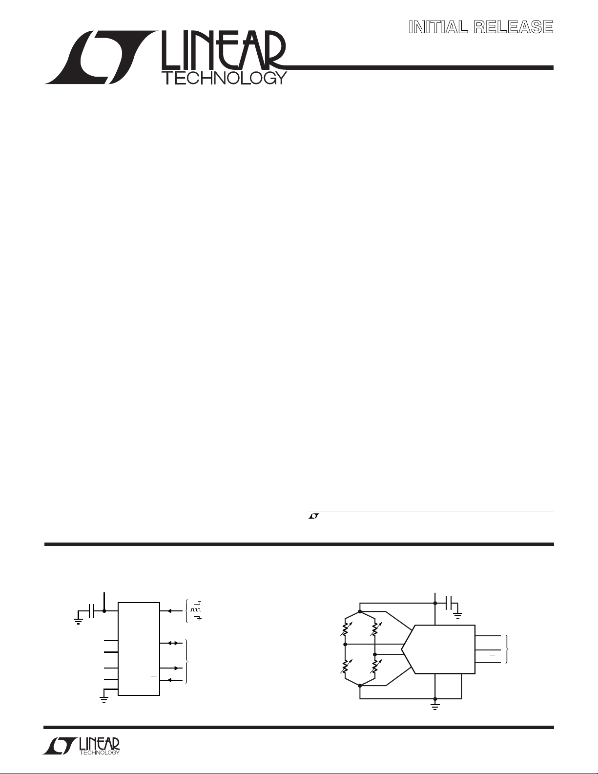
TYPICAL APPLICATIO S
2.7V TO 5.5V
1µF
214
V
CC
LTC2410
3
REFERENCE
VOLTAGE
0.1V TO V
CC
ANALOG INPUT RANGE
TO 0.5V
–0.5V
REF
REF
1, 7, 8, 9, 10, 15, 16
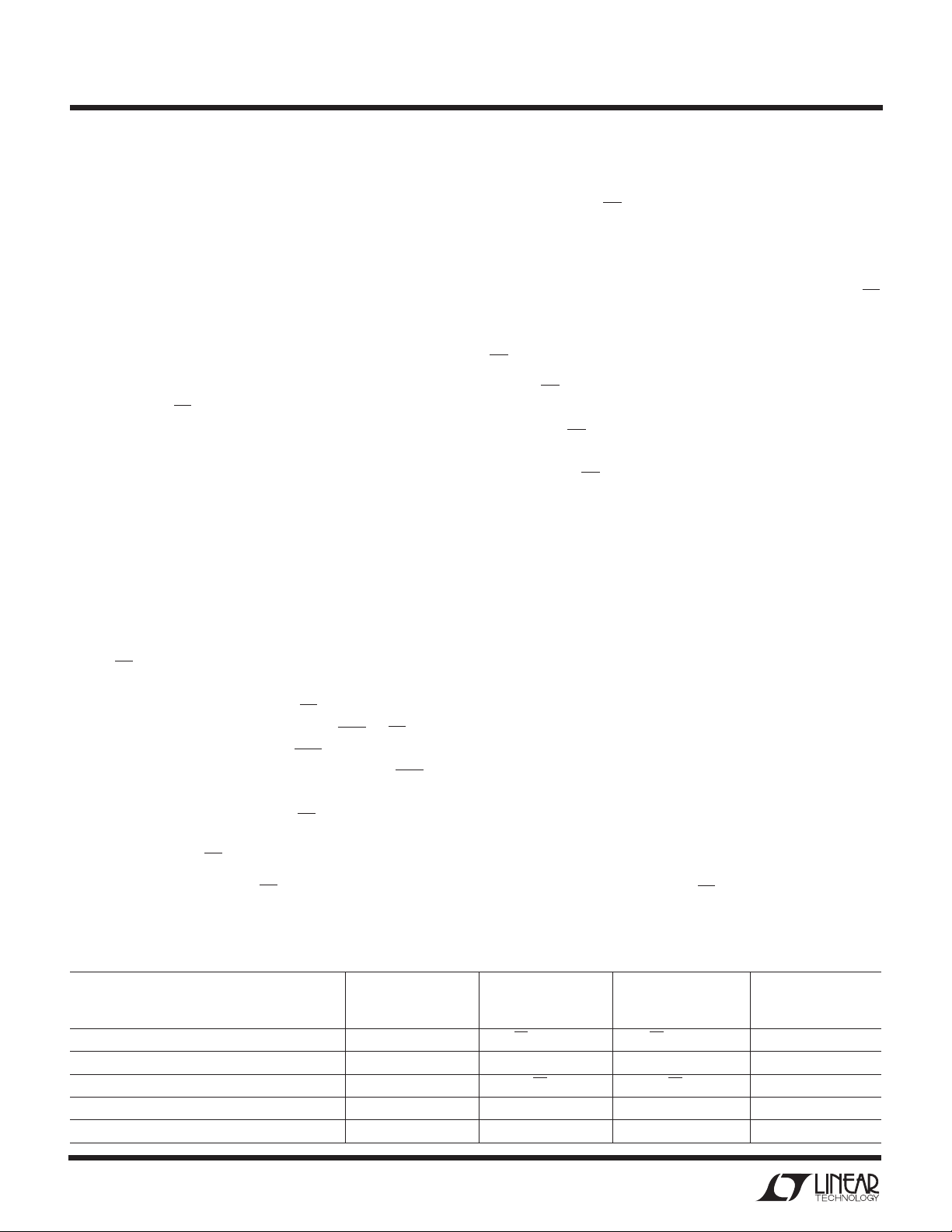
+
REF
REF
IN
IN
GND
SCK
–
+
SDO
–
4
5
6
U
V
CC
= INTERNAL OSC/50Hz REJECTION
F
O
13
12
11
CS
Information furnished by Linear Technology Corporation is believed to be accurate and reliable.
However, no responsibility is assumed for its use. Linear Technology Corporation makes no representation that the interconnection of its circuits as described herein will not infringe on existing patent rights.
= EXTERNAL CLOCK SOURCE
= INTERNAL OSC/60Hz REJECTION
3-WIRE
SPI INTERFACE
2410 TA01
BRIDGE
IMPEDANCE
100Ω TO10k
V
CC
1µF
2
3
REF+V
IN
IN
+
–
REF
CC
LTC2410
–
GND F
1, 7, 8
9, 10,
15, 16
5
6
4
12
SDO
3-WIRE
SCK
13
11
O
14
2410 TA02
CS
SPI INTERFACE
1
LTC2410
WW
W
ABSOLUTE AXI U RATI GS
U
UUW
PACKAGE/ORDER I FOR ATIO
(Notes 1, 2)
Supply Voltage (VCC) to GND.......................– 0.3V to 7V
Analog Input Pins Voltage
to GND.................................... –0.3V to (VCC + 0.3V)
Reference Input Pins Voltage
to GND.................................... –0.3V to (VCC + 0.3V)
Digital Input Voltage to GND........ –0.3V to (VCC + 0.3V)
Digital Output Voltage to GND ..... –0.3V to (VCC + 0.3V)
Operating Temperature Range
GND
REF
REF
GND
GND
V
CC
IN
IN
LTC2410C ............................................... 0°C to 70°C
LTC2410I............................................ –40°C to 85°C
Storage Temperature Range ................. –65°C to 150°C
Lead Temperature (Soldering, 10 sec).................. 300°C
ELECTRICAL CHARACTERISTICS
temperature range, otherwise specifications are at T
PARAMETER CONDITIONS MIN TYP MAX UNITS
Resolution (No Missing Codes) 0.1V ≤ V
Integral Nonlinearity REF+ = 2.5V, REF– = GND, V
5V ≤ VCC ≤ 5.5V, REF+ = 5V, REF– = GND, V
Offset Error 2.5V ≤ REF+ ≤ VCC, REF– = GND, ● 0.5 2.5 µV
GND ≤ IN
Offset Error Drift 2.5V ≤ REF+ ≤ VCC, REF– = GND, 10 nV/°C
GND ≤ IN
Positive Full-Scale Error 2.5V ≤ REF+ ≤ VCC, REF– = GND, ● 2.5 12 ppm of V
IN+ = 0.75REF+, IN– = 0.25 • REF
Positive Full-Scale Error Drift 2.5V ≤ REF+ ≤ VCC, REF– = GND, 0.04 ppm of V
Negative Full-Scale Error 2.5V ≤ REF+ ≤ VCC, REF– = GND, ● 2.5 12 ppm of V
Negative Full-Scale Error Drift 2.5V ≤ REF+ ≤ VCC, REF– = GND, 0.04 ppm of V
Total Unadjusted Error REF+ = 2.5V, REF– = GND, V
Output Noise 5V ≤ VCC ≤ 5.5V, REF+ = 5V, V
+
IN
IN+ = 0.25 • REF+, IN– = 0.75 • REF
+
IN
5V ≤ VCC ≤ 5.5V, REF+ = 5V, REF– = GND, V
GND ≤ IN– = IN+ ≤ 5V, (Note 13)
≤ VCC, –0.5 • V
REF
+
= IN– ≤ VCC, (Note 14)
+
= IN– ≤ V
= 0.75REF+, IN– = 0.25 • REF
= 0.25 • REF+, IN– = 0.75 • REF
The ● denotes specifications which apply over the full operating
= 25°C. (Notes 3, 4)
A
≤ VIN ≤ 0.5 • V
REF
= 1.25V, (Note 6) ● 1 ppm of V
INCM
CC
= 1.25V 5 ppm of V
INCM
REF
Consult factory for Military grade parts.
REF
= 2.5V, (Note 6) ● 2 14 ppm of V
INCM
+
+
+
+
= 2.5V 10 ppm of V
INCM
– = GND, 0.8 µV
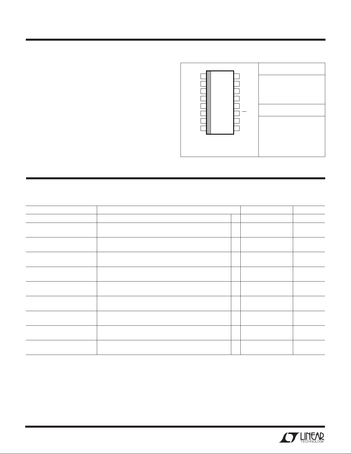
TOP VIEW
1
2
+
3
–
4
+
5
–
6
7
8
GN PACKAGE
16-LEAD PLASTIC SSOP
T
= 125°C, θJA = 95°C/W
JMAX
, (Note 5) ● 24 Bits
16
GND
15
GND
14
F
O
13
SCK
12
SDO
11
CS
10
GND
9
GND
ORDER PART NUMBER
LTC2410CGN
LTC2410IGN
GN PART MARKING
2410
2410I
REF
REF
REF
/°C
REF
REF
/°C
REF
REF
REF
RMS
2

LTC2410
U
CO VERTER CHARACTERISTICS
temperature range, otherwise specifications are at T
PARAMETER CONDITIONS MIN TYP MAX UNITS
Input Common Mode Rejection DC 2.5V ≤ REF+ ≤ VCC, REF– = GND, ● 130 140 dB
GND ≤ IN
Input Common Mode Rejection 2.5V ≤ REF+ ≤ VCC, REF– = GND, ● 140 dB
60Hz ±2% GND ≤ IN
Input Common Mode Rejection 2.5V ≤ REF+ ≤ VCC, REF– = GND, ● 140 dB
50Hz ±2% GND ≤ IN
Input Normal Mode Rejection (Note 7) ● 110 140 dB
60Hz ±2%
Input Normal Mode Rejection (Note 8) ● 110 140 dB
50Hz ±2%
Reference Common Mode 2.5V ≤ REF+ ≤ VCC, GND ≤ REF– ≤ 2.5V, ● 130 140 dB
Rejection DC V
Power Supply Rejection, DC REF+ = 2.5V, REF– = GND, IN– = IN+ = GND 100 dB
Power Supply Rejection, 60Hz ±2% REF+ = 2.5V, REF– = GND, IN– = IN+ = GND, (Note 7) 110 dB
Power Supply Rejection, 50Hz ±2% REF+ = 2.5V, REF– = GND, IN– = IN+ = GND, (Note 8) 110 dB
–
= IN+ ≤ 5V
–
= IN+ ≤ 5V, (Note 7)
–
= IN+ ≤ 5V, (Note 8)
= 2.5V, IN– = IN+ = GND
REF
The ● denotes specifications which apply over the full operating
= 25°C. (Notes 3, 4)
A
UUU
A ALOG I PUT AUD REFERE CE
temperature range, otherwise specifications are at T
SYMBOL PARAMETER CONDITIONS MIN TYP MAX UNITS
+
IN
–
IN
V
IN
+
REF
–
REF
V
REF
CS (IN+)IN
CS (IN–)IN
CS (REF+)REF
CS (REF–)REF
I
I
I
I
(IN+)IN+ DC Leakage Current CS = VCC, IN+ = GND ● –10 1 10 nA
DC_LEAK
(IN–)IN– DC Leakage Current CS = VCC, IN– = GND ● –10 1 10 nA
DC_LEAK
(REF+)REF+ DC Leakage Current CS = VCC, REF+ = 5V ● –10 1 10 nA
DC_LEAK
(REF–)REF– DC Leakage Current CS = VCC, REF– = GND ● –10 1 10 nA
DC_LEAK
Absolute/Common Mode IN+ Voltage ● GND – 0.3V VCC + 0.3V V
Absolute/Common Mode IN– Voltage ● GND – 0.3V VCC + 0.3V V
Input Differential Voltage Range ● –V
+
(IN
– IN–)
Absolute/Common Mode REF+ Voltage ● 0.1 V
Absolute/Common Mode REF– Voltage ● GND VCC – 0.1V V
Reference Differential Voltage Range ● 0.1 V
+
– REF–)
(REF
+
Sampling Capacitance 18 pF
–
Sampling Capacitance 18 pF
+
Sampling Capacitance 18 pF
–
Sampling Capacitance 18 pF
= 25°C. (Note 3)
A
The ● denotes specifications which apply over the full operating
/2 V
REF
/2 V
REF
CC
CC
V
V
3
LTC2410
UU
DIGITAL I PUTS A D DIGITAL OUTPUTS
operating temperature range, otherwise specifications are at T
SYMBOL PARAMETER CONDITIONS MIN TYP MAX UNITS
V
IH
V
IL
V
IH
V
IL
I
IN
I
IN
C
IN
C
IN
V
OH
V
OL
V
OH
V
OL
I
OZ
High Level Input Voltage 2.7V ≤ VCC ≤ 5.5V ● 2.5 V
CS, F
O
Low Level Input Voltage 4.5V ≤ VCC ≤ 5.5V ● 0.8 V
CS, F
O
High Level Input Voltage 2.7V ≤ VCC ≤ 5.5V (Note 9) ● 2.5 V
SCK 2.7V ≤ V
Low Level Input Voltage 4.5V ≤ VCC ≤ 5.5V (Note 9) ● 0.8 V
SCK 2.7V ≤ V
Digital Input Current 0V ≤ VIN ≤ V
CS, F
O
Digital Input Current 0V ≤ VIN ≤ VCC (Note 9) ● –10 10 µA
SCK
Digital Input Capacitance 10 pF
CS, F
O
Digital Input Capacitance (Note 9) 10 pF
SCK
High Level Output Voltage IO = –800µA ● VCC – 0.5V V
SDO
Low Level Output Voltage IO = 1.6mA ● 0.4V V
SDO
High Level Output Voltage IO = –800µA (Note 10) ● VCC – 0.5V V
SCK
Low Level Output Voltage IO = 1.6mA (Note 10) ● 0.4V V
SCK
Hi-Z Output Leakage ● –10 10 µA
SDO
2.7V ≤ VCC ≤ 3.3V 2.0 V
2.7V ≤ VCC ≤ 5.5V 0.6 V
= 25°C. (Note 3)
A
≤ 3.3V (Note 9) 2.0 V
CC
≤ 5.5V (Note 9) 0.6 V
CC
CC
The ● denotes specifications which apply over the full
● –10 10 µA
WU
POWER REQUIRE E TS
otherwise specifications are at T
SYMBOL PARAMETER CONDITIONS MIN TYP MAX UNITS
V
CC
I
CC
Supply Voltage ● 2.7 5.5 V
Supply Current
Conversion Mode CS = 0V (Note 12)
Sleep Mode CS = V
= 25°C. (Note 3)
A
The ● denotes specifications which apply over the full operating temperature range,
● 200 300 µA
(Note 12) ● 20 30 µA
CC
4
LTC2410
WU
TI I G CHARACTERISTICS
range, otherwise specifications are at T
SYMBOL PARAMETER CONDITIONS MIN TYP MAX UNITS
f
EOSC
t
HEO
t
LEO
t
CONV
f
ISCK
D
ISCK
f
ESCK
t
LESCK
t
HESCK
t
DOUT_ISCK
t
DOUT_ESCK
t
1
t2 CS ↑ to SDO High Z ● 0 200 ns
t3 CS ↓ to SCK ↓ (Note 10) ● 0 200 ns
t4 CS ↓ to SCK ↑ (Note 9) ● 50 ns
t
KQMAX
t
KQMIN
t
5
t
6
Note 1: Absolute Maximum Ratings are those values beyond which the
life of the device may be impaired.
Note 2: All voltage values are with respect to GND.
Note 3: V
= REF+ – REF–, V
V
REF
V
= IN+ – IN–, V
IN
Note 4: F
source with f
Note 5: Guaranteed by design, not subject to test.
Note 6: Integral nonlinearity is defined as the deviation of a code from
a straight line passing through the actual endpoints of the transfer
curve. The deviation is measured from the center of the quantization
band.
Note 7: FO = 0V (internal oscillator) or f
(external oscillator).
External Oscillator Frequency Range ● 2.56 2000 kHz
External Oscillator High Period ● 0.25 390 µs
External Oscillator Low Period ● 0.25 390 µs
Conversion Time FO = 0V ● 130.86 133.53 136.20 ms
Internal SCK Frequency Internal Oscillator (Note 10) 19.2 kHz
Internal SCK Duty Cycle (Note 10) ● 45 55 %
External SCK Frequency Range (Note 9) ● 2000 kHz
External SCK Low Period (Note 9) ● 250 ns
External SCK High Period (Note 9) ● 250 ns
Internal SCK 32-Bit Data Output Time Internal Oscillator (Notes 10, 12) ● 1.64 1.67 1.70 ms
External SCK 32-Bit Data Output Time (Note 9) ● 32/f
CS ↓ to SDO Low Z ● 0 200 ns
SCK ↓ to SDO Valid ● 220 ns
SDO Hold After SCK ↓ (Note 5) ● 15 ns
SCK Set-Up Before CS ↓ ● 50 ns
SCK Hold After CS ↓ ● 50 ns
= 2.7 to 5.5V unless otherwise specified.
CC
INCM
pin tied to GND or to VCC or to external conversion clock
O
= 153600Hz unless otherwise specified.
EOSC
= (REF+ + REF–)/2;
REFCM
= (IN+ + IN–)/2.
= 25°C. (Note 3)
A
= 153600Hz ±2%
EOSC
The ● denotes specifications which apply over the full operating temperature
F
= V
O
CC
External Oscillator (Note 11)
External Oscillator (Notes 10, 11) f
External Oscillator (Notes 10, 11)
Note 8: FO = VCC (internal oscillator) or f
(external oscillator).
Note 9: The converter is in external SCK mode of operation such that
the SCK pin is used as digital input. The frequency of the clock signal
driving SCK during the data output is f
Note 10: The converter is in internal SCK mode of operation such that
the SCK pin is used as digital output. In this mode of operation the
SCK pin has a total equivalent load capacitance C
Note 11: The external oscillator is connected to the FO pin. The external
oscillator frequency, f
Note 12: The converter uses the internal oscillator.
= 0V or FO = VCC.
F
O
Note 13: The output noise includes the contribution of the internal
calibration operations.
Note 14: Guaranteed by design and test correlation.
● 157.03 160.23 163.44 ms
● 20510/f
● 256/f
, is expressed in kHz.
EOSC
(in kHz) ms
EOSC
/8 kHz
EOSC
(in kHz) ms
EOSC
(in kHz) ms
ESCK
= 128000Hz ±2%
EOSC
and is expressed in kHz.
ESCK
= 20pF.
LOAD
5

LTC2410
UUU
PI FU CTIO S
GND (Pins 1, 7, 8, 9, 10, 15, 16): Ground. Multiple
ground pins internally connected for optimum ground
current flow and VCC decoupling. Connect each one of
these pins to a ground plane through a low impedance
connection.
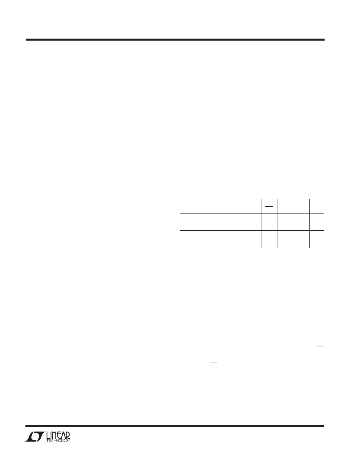
VCC (Pin 2): Positive Supply Voltage. Bypass to GND
(Pin␣ 1) with a 10µF tantalum capacitor in parallel with
0.1µF ceramic capacitor as close to the part as possible.
REF+ (Pin 3), REF– (Pin 4): Differential Reference Input.
The voltage on these pins can have any value between GND
and VCC as long as the reference positive input, REF+, is
maintained more positive than the reference negative
input, REF–, by at least 0.1V.
IN+ (Pin 5), IN– (Pin 6): Differential Analog Input. The
voltage on these pins can have any value between
GND – 0.3V and VCC + 0.3V. Within these limits the
converter bipolar input range (VIN = IN+ – IN–) extends
from – 0.5 • (V
the converter produces unique overrange and underrange
output codes.
CS (Pin 11): Active LOW Digital Input. A LOW on this pin
enables the SDO digital output and wakes up the ADC.
Following each conversion the ADC automatically enters
the Sleep mode and remains in this low power state as
long as CS is HIGH. A LOW-to-HIGH transition on CS
during the Data Output transfer aborts the data transfer
and starts a new conversion.
) to 0.5 • (V
REF
). Outside this input range
REF
SDO (Pin 12): Three-State Digital Output. During the Data
Output period this pin is used as serial data output. When
the chip select CS is HIGH (CS = VCC) the SDO pin is in a
high impedance state. During the Conversion and Sleep
periods this pin is used as the conversion status output.
The conversion status can be observed by pulling CS LOW.
SCK (Pin 13): Bidirectional Digital Clock Pin. In Internal
Serial Clock Operation mode, SCK is used as digital output
for the internal serial interface clock during the Data
Output period. In External Serial Clock Operation mode,
SCK is used as digital input for the external serial interface
clock during the Data Output period. A weak internal pullup is automatically activated in Internal Serial Clock Operation mode. The Serial Clock Operation mode is determined by the logic level applied to the SCK pin at power up
or during the most recent falling edge of CS.
FO (Pin 14): Frequency Control Pin. Digital input that
controls the ADC’s notch frequencies and conversion
time. When the FO pin is connected to VCC (FO = VCC), the
converter uses its internal oscillator and the digital filter
first null is located at 50Hz. When the FO pin is connected
to GND (FO = OV), the converter uses its internal oscillator
and the digital filter first null is located at 60Hz. When F
is driven by an external clock signal with a frequency f
the converter uses this signal as its system clock and the
digital filter first null is located at a frequency f
EOSC
EOSC
/2560.
O
,
6
LTC2410
1.69k
SDO
2410 TA04
Hi-Z TO V
OL
VOH TO V
OL
VOL TO Hi-Z
C
LOAD
= 20pF
V
CC
CONVERT
SLEEP
DATA OUTPUT
2410 F01
TRUE
FALSE
CS = LOW
AND
SCK
UU
W
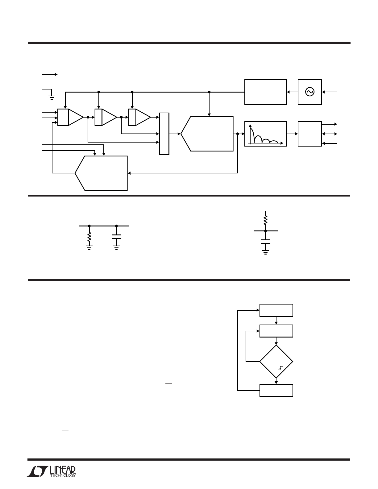
FU CTIO AL BLOCK DIAGRA
V
CC
GND
+
IN
–
IN
+
–
∫∫∫
∑
+
REF
–
REF
–+
DAC
TEST CIRCUITS
SDO
ADC
AUTOCALIBRATION
AND CONTROL
DECIMATING FIR
INTERNAL
OSCILLATOR
SERIAL
INTERFACE
(INT/EXT)
F
O
SDO
SCK
CS
2410 FD
1.69k
Hi-Z TO V
VOL TO V
OH
VOH TO Hi-Z
U
OH
= 20pF
C
LOAD
2410 TA03
WUU
APPLICATIO S I FOR ATIO
CONVERTER OPERATION
Converter Operation Cycle
The LTC2410 is a low power, delta-sigma analog-todigital converter with an easy to use 3-wire serial interface.
Its operation is made up of three states. The converter
operating cycle begins with the conversion, followed by
the low power sleep state and ends with the data output
(see Figure 1). The 3-wire interface consists of serial data
output (SDO), serial clock (SCK) and chip select (CS).
Initially, the LTC2410 performs a conversion. Once the
conversion is complete, the device enters the sleep state.
While in this sleep state, power consumption is reduced by
an order of magnitude. The part remains in the sleep state
as long as CS is HIGH. The conversion result is held
indefinitely in a static shift register while the converter is
in the sleep state.
Figure 1. LTC2410 State Transition Diagram
7

LTC2410
U
WUU
APPLICATIO S I FOR ATIO
Once CS is pulled LOW, the device begins outputting the
conversion result. There is no latency in the conversion
result. The data output corresponds to the conversion just
performed. This result is shifted out on the serial data out
pin (SDO) under the control of the serial clock (SCK). Data
is updated on the falling edge of SCK allowing the user to
reliably latch data on the rising edge of SCK (see Figure 3).
The data output state is concluded once 32 bits are read
out of the ADC or when CS is brought HIGH. The device
automatically initiates a new conversion and the cycle
repeats.
Through timing control of the CS and SCK pins, the
LTC2410 offers several flexible modes of operation
(internal or external SCK and free-running conversion
modes). These various modes do not require programming configuration registers; moreover, they do not disturb the cyclic operation described above. These modes of
operation are described in detail in the Serial Interface
Timing Modes section.
Conversion Clock
A major advantage the delta-sigma converter offers over
conventional type converters is an on-chip digital filter
(commonly implemented as a Sinc or Comb filter). For
high resolution, low frequency applications, this filter is
typically designed to reject line frequencies of 50 or 60Hz
plus their harmonics. The filter rejection performance is
directly related to the accuracy of the converter system
clock. The LTC2410 incorporates a highly accurate onchip oscillator. This eliminates the need for external frequency setting components such as crystals or oscillators. Clocked by the on-chip oscillator, the LTC2410
achieves a minimum of 110dB rejection at the line frequency (50Hz or 60Hz ±2%).
Ease of Use
The LTC2410 data output has no latency, filter settling
delay or redundant data associated with the conversion
cycle. There is a one-to-one correspondence between the
conversion and the output data. Therefore, multiplexing
multiple analog voltages is easy.
The LTC2410 performs offset and full-scale calibrations
every conversion cycle. This calibration is transparent to
the user and has no effect on the cyclic operation described above. The advantage of continuous calibration is
extreme stability of offset and full-scale readings with respect to time, supply voltage change and temperature drift.
Power-Up Sequence
The LTC2410 automatically enters an internal reset state
when the power supply voltage VCC drops below approximately 2.2V. This feature guarantees the integrity of the
conversion result and of the serial interface mode selection. (See the 2-wire I/O sections in the Serial Interface
Timing Modes section.)
When the VCC voltage rises above this critical threshold,
the converter creates an internal power-on-reset (POR)
signal with a duration of approximately 0.5ms. The POR
signal clears all internal registers. Following the POR
signal, the LTC2410 starts a normal conversion cycle and
follows the succession of states described above. The first
conversion result following POR is accurate within the
specifications of the device if the power supply voltage is
restored within the operating range (2.7V to 5.5V) before
the end of the POR time interval.
Reference Voltage Range
This converter accepts a truly differential external reference voltage. The absolute/common mode voltage specification for the REF+ and REF– pins covers the entire range
from GND to VCC. For correct converter operation, the
REF+ pin must always be more positive than the REF– pin.
The LTC2410 can accept a differential reference voltage
from 0.1V to VCC. The converter output noise is determined by the thermal noise of the front-end circuits, and
as such, its value in nanovolts is nearly constant with
reference voltage. A decrease in reference voltage will not
significantly improve the converter’s effective resolution.
On the other hand, a reduced reference voltage will improve the converter’s overall INL performance. A reduced
reference voltage will also improve the converter performance when operated with an external conversion clock
(external FO signal) at substantially higher output data
rates (see the Output Data Rate section).
8
LTC2410
U
WUU
APPLICATIO S I FOR ATIO
Input Voltage Range
The analog input is truly differential with an absolute/
common mode range for the IN+ and IN– input pins
extending from GND – 0.3V to VCC + 0.3V. Outside
these limits the ESD protection devices begin to turn on
and the errors due to input leakage current increase
rapidly. Within these limits the LTC2410 converts the
bipolar differential input signal, VIN = IN+ – IN–, from
–FS = – 0.5 • V
REF+ – REF–. Outside this range the converter indicates the
overrange or the underrange condition using distinct
output codes.
Input signals applied to IN+ and IN– pins may extend by
300mV below ground and above VCC. In order to limit any
fault current, resistors of up to 5k may be added in series
with the IN+ and IN– pins without affecting the performance of the device. In the physical layout, it is important
to maintain the parasitic capacitance of the connection
between these series resistors and the corresponding pins
as low as possible; therefore, the resistors should be
located as close as practical to the pins. The effect of the
series resistance on the converter accuracy can be evaluated from the curves presented in the Input Current/
Reference Current sections. In addition, series resistors
will introduce a temperature dependent offset error due to
the input leakage current. A 1nA input leakage current will
develop a 1ppm offset error on a 5k resistor if V
This error has a very strong temperature dependency.
Output Data Format
The LTC2410 serial output data stream is 32 bits long. The
first 3 bits represent status information indicating the sign
and conversion state. The next 24 bits are the conversion
result, MSB first. The remaining 5 bits are sub LSBs
beyond the 24-bit level that may be included in averaging
or discarded without loss of resolution. The third and
fourth bit together are also used to indicate an underrange
condition (the differential input voltage is below –FS) or an
overrange condition (the differential input voltage is above
+FS).
Bit 31 (first output bit) is the end of conversion (EOC)
indicator. This bit is available at the SDO pin during the
conversion and sleep states whenever the CS pin is LOW.
to +FS = 0.5 • V
REF
where V
REF
REF
=
REF
= 5V.
This bit is HIGH during the conversion and goes LOW
when the conversion is complete.
Bit 30 (second output bit) is a dummy bit (DMY) and is
always LOW.
Bit 29 (third output bit) is the conversion result sign indicator (SIG). If VIN is >0, this bit is HIGH. If VIN is <0, this
bit is LOW.
Bit 28 (fourth output bit) is the most significant bit (MSB)
of the result. This bit in conjunction with Bit 29 also
provides the underrange or overrange indication. If both
Bit 29 and Bit 28 are HIGH, the differential input voltage is
above +FS. If both Bit 29 and Bit 28 are LOW, the
differential input voltage is below –FS.
The function of these bits is summarized in Table 1.
Table 1. LTC2410 Status Bits
Bit 31 Bit 30 Bit 29 Bit 28
Input Range EOC DMY SIG MSB
VIN ≥ 0.5 • V
0V ≤ VIN < 0.5 • V
–0.5 • V
VIN < –0.5 • V
REF
≤ VIN < 0V 0 0 0 1
REF
REF
REF
0011
0010
0000
Bits 28-5 are the 24-bit conversion result MSB first.
Bit 5 is the least significant bit (LSB).
Bits 4-0 are sub LSBs below the 24-bit level. Bits 4-0 may
be included in averaging or discarded without loss of
resolution.
Data is shifted out of the SDO pin under control of the serial
clock (SCK), see Figure 3. Whenever CS is HIGH, SDO
remains high impedance and any externally generated
SCK clock pulses are ignored by the internal data out shift
register.
In order to shift the conversion result out of the device, CS
must first be driven LOW. EOC is seen at the SDO pin of the
device once CS is pulled LOW. EOC changes real time from
HIGH to LOW at the completion of a conversion. This
signal may be used as an interrupt for an external
microcontroller. Bit 31 (EOC) can be captured on the first
rising edge of SCK. Bit 30 is shifted out of the device on the
first falling edge of SCK. The final data bit (Bit 0) is shifted
out on the falling edge of the 31st SCK and may be latched
9
LTC2410
U
WUU
APPLICATIO S I FOR ATIO
on the rising edge of the 32nd SCK pulse. On the falling
edge of the 32nd SCK pulse, SDO goes HIGH indicating the
initiation of a new conversion cycle. This bit serves as EOC
(Bit 31) for the next conversion cycle. Table 2 summarizes
the output data format.
As long as the voltage on the IN+ and IN– pins is maintained
within the –0.3V to (VCC + 0.3V) absolute maximum
operating range, a conversion result is generated for any
differential input voltage VIN from –FS = –0.5 • V
+FS = 0.5 • V
. For differential input voltages greater than
REF
+FS, the conversion result is clamped to the value corresponding to the +FS + 1LSB. For differential input voltages
below –FS, the conversion result is clamped to the value
corresponding to –FS – 1LSB.
CS
REF
to
Frequency Rejection Selection (FO)
The LTC2410 internal oscillator provides better than 110dB
normal mode rejection at the line frequency and all its
harmonics for 50Hz ±2% or 60Hz ±2%. For 60Hz rejection, FO should be connected to GND while for 50Hz
rejection the FO pin should be connected to VCC.
The selection of 50Hz or 60Hz rejection can also be made
by driving FO to an appropriate logic level. A selection
change during the sleep or data output states will not
disturb the converter operation. If the selection is made
during the conversion state, the result of the conversion in
progress may be outside specifications but the following
conversions will not be affected.
When a fundamental rejection frequency different from
50Hz or 60Hz is required or when the converter must be
BIT 31
SDO
Hi-Z
SCK
SLEEP DATA OUTPUT CONVERSION
Table 2. LTC2410 Output Data Format
Differential Input Voltage Bit 31 Bit 30 Bit 29 Bit 28 Bit 27 Bit 26 Bit 25 … Bit 0
* EOC DMY SIG MSB
V
IN
VIN* ≥ 0.5 • V
0.5 • V
0.25 • V
0.25 • V
0 00100 0 0…0
–1LSB 0 0011 1 1…1
–0.25 • V
–0.25 • V
–0.5 • V
VIN* < –0.5 • V
*The differential input voltage VIN = IN+ – IN–.
**The differential reference voltage V
REF
** – 1LSB 0 0101 1 1…1
REF
** 00101 0 0…0
REF
** – 1LSB 00100 1 1…1
REF
** 00011 0 0…0
REF
** – 1LSB 00010 1 1…1
REF
** 00010 0 0…0
REF
REF
EOC
12345 262732
** 00110 0 0…0
** 00001 1 1…1
= REF+ – REF–.
REF
BIT 28BIT 29BIT 30
MSBSIG“0”
Figure 3. Output Data Timing
LSB
BIT 0BIT 27 BIT 5
24
2410 F03
10
LTC2410
U
WUU
APPLICATIO S I FOR ATIO
synchronized with an outside source, the LTC2410 can
operate with an external conversion clock. The converter
automatically detects the presence of an external clock
signal at the FO pin and turns off the internal oscillator. The
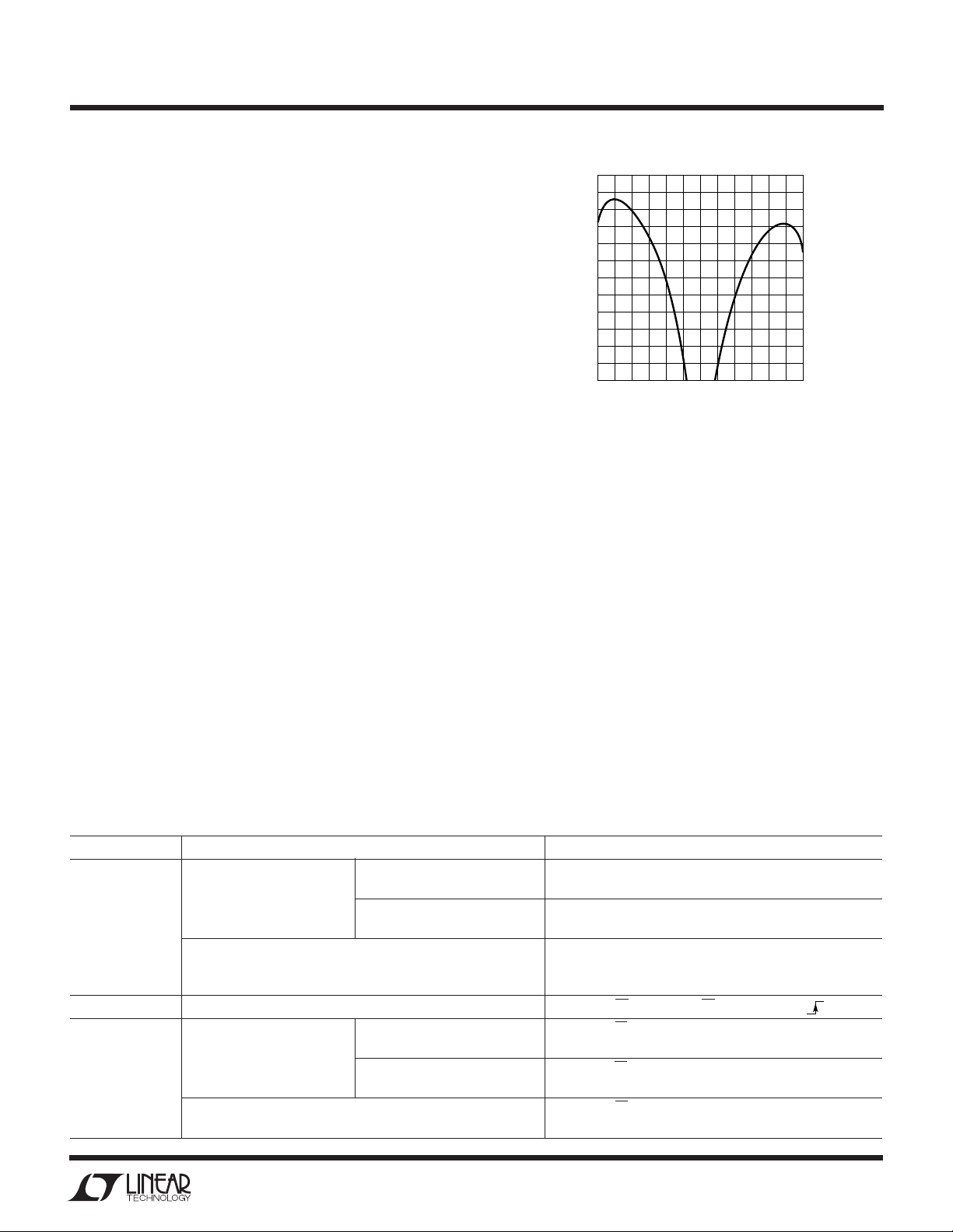
frequency f
2560Hz (1Hz notch frequency) to be detected. The external clock signal duty cycle is not significant as long as the
minimum and maximum specifications for the high and
low periods t
While operating with an external conversion clock of a
frequency f
normal mode rejection in a frequency range f
±4% and its harmonics. The normal mode rejection as a
function of the input frequency deviation from f
is shown in Figure 4.
Whenever an external clock is not present at the FO pin the
converter automatically activates its internal oscillator and
enters the Internal Conversion Clock mode. The LTC2410
operation will not be disturbed if the change of conversion
clock source occurs during the sleep state or during the
data output state while the converter uses an external
serial clock. If the change occurs during the conversion
state, the result of the conversion in progress may be
outside specifications but the following conversions will
not be affected. If the change occurs during the data output
state and the converter is in the Internal SCK mode, the
serial clock duty cycle may be affected but the serial data
stream will remain valid.
of the external signal must be at least
EOSC
and t
HEO
, the LTC2410 provides better than 110dB
EOSC
are observed.
LEO
EOSC
EOSC
/2560
/2560
–80
–85
–90
–95
–100
–105
–110
–115
–120
–125
NORMAL MODE REJECTION (dB)
–130
–135
–140
–12–8–404812
DIFFERENTIAL INPUT SIGNAL FREQUENCY
DEVIATION FROM NOTCH FREQUENCY f
Figure 4. LTC2410 Normal Mode Rejection When
Using an External Oscillator of Frequency f
EOSC
/2560(%)
2410 F04
EOSC
Table 3 summarizes the duration of each state and the
achievable output data rate as a function of FO.
SERIAL INTERFACE PINS
The LTC2410 transmits the conversion results and receives the start of conversion command through a synchronous 3-wire interface. During the conversion and
sleep states, this interface can be used to assess the
converter status and during the data output state it is used
to read the conversion result.
Table 3. LTC2410 State Duration
State Operating Mode Duration
CONVERT Internal Oscillator FO = LOW 133ms, Output Data Rate ≤ 7.5 Readings/s
(60Hz Rejection)
FO = HIGH 160ms, Output Data Rate ≤ 6.2 Readings/s
(50Hz Rejection)
External Oscillator FO = External Oscillator 20510/f
with Frequency f
/2560 Rejection)
(f
EOSC
SLEEP As Long As CS = HIGH Until CS = LOW and SCK
DATA OUTPUT Internal Serial Clock FO = LOW/HIGH As Long As CS = LOW But Not Longer Than 1.67ms
(Internal Oscillator) (32 SCK cycles)
FO = External Oscillator with As Long As CS = LOW But Not Longer Than 256/f
Frequency f
External Serial Clock with As Long As CS = LOW But Not Longer Than 32/f
Frequency f
kHz (32 SCK cycles)
SCK
EOSC
kHz
EOSC
kHz (32 SCK cycles)
s, Output Data Rate ≤ f
EOSC
/20510 Readings/s
EOSC
SCK
EOSC
ms
ms
11
LTC2410
U
WUU
APPLICATIO S I FOR ATIO
Serial Clock Input/Output (SCK)
The serial clock signal present on SCK (Pin 13) is used to
synchronize the data transfer. Each bit of data is shifted out
the SDO pin on the falling edge of the serial clock.
In the Internal SCK mode of operation, the SCK pin is an
output and the LTC2410 creates its own serial clock by
dividing the internal conversion clock by 8. In the External
SCK mode of operation, the SCK pin is used as input. The
internal or external SCK mode is selected on power-up and
then reselected every time a HIGH-to-LOW transition is
detected at the CS pin. If SCK is HIGH or floating at powerup or during this transition, the converter enters the internal SCK mode. If SCK is LOW at power-up or during this
transition, the converter enters the external SCK mode.
Serial Data Output (SDO)
The serial data output pin, SDO (Pin 12), provides the
result of the last conversion as a serial bit stream (MSB
first) during the data output state. In addition the SDO pin
is used as an end of conversion indicator during the
conversion and sleep states.
When CS (Pin 11) is HIGH, the SDO driver is switched to
a high impedance state. This allows sharing the serial
interface with other devices. If CS is LOW during the
convert or sleep state, SDO will output EOC. If CS is LOW
during the conversion phase, the EOC bit appears HIGH on
the SDO pin. Once the conversion is complete, EOC goes
LOW. The device remains in the sleep state until the first
rising edge of SCK occurs while CS = LOW.
Chip Select Input (CS)
The active LOW chip select, CS (Pin 11), is used to test the
conversion status and to enable the data output transfer as
described in the previous sections.
In addition, the CS signal can be used to trigger a new
conversion cycle before the entire serial data transfer has
been completed. The LTC2410 will abort any serial data
transfer in progress and start a new conversion cycle
anytime a LOW-to-HIGH transition is detected at the CS
pin after the converter has entered the data output state
(i.e., after the first rising edge of SCK occurs with
CS␣=␣LOW).
Finally, CS can be used to control the free-running modes
of operation, see Serial Interface Timing Modes section.
Grounding CS will force the ADC to continuously convert
at the maximum output rate selected by FO. Tying a
capacitor to CS will reduce the output rate and power
dissipation by a factor proportional to the capacitor’s
value, see Figures 12 to 14.
SERIAL INTERFACE TIMING MODES
The LTC2410’s 3-wire interface is SPI and MICROWIRE
compatible. This interface offers several flexible modes of
operation. These include internal/external serial clock,
2- or 3-wire I/O, single cycle conversion and autostart. The
following sections describe each of these serial interface
timing modes in detail. In all these cases, the converter
can use the internal oscillator (FO = LOW or FO = HIGH) or
an external oscillator connected to the FO pin. Refer to
Table␣ 4 for a summary.
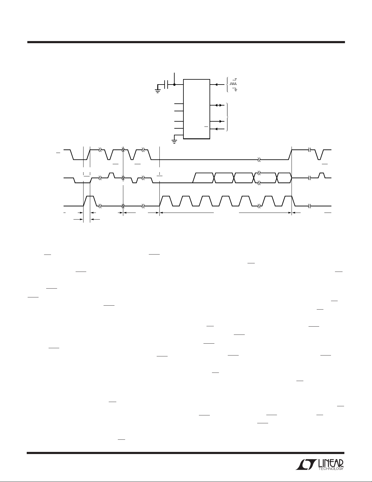
External Serial Clock, Single Cycle Operation
(SPI/MICROWIRE Compatible)
This timing mode uses an external serial clock to shift out
the conversion result and a CS signal to monitor and
control the state of the conversion cycle, see Figure 5.
Table 4. LTC2410 Interface Timing Modes
Conversion Data Connection
SCK Cycle Output and
Configuration Source Control Control Waveforms
External SCK, Single Cycle Conversion External CS and SCK CS and SCK Figures 5, 6
External SCK, 2-Wire I/O External SCK SCK Figure 7
Internal SCK, Single Cycle Conversion Internal CS ↓ CS ↓ Figures 8, 9
Internal SCK, 2-Wire I/O, Continuous Conversion Internal Continuous Internal Figure 10
Internal SCK, Autostart Conversion Internal C
EXT
Internal Figure 11
12
LTC2410
U
WUU
APPLICATIO S I FOR ATIO
The serial clock mode is selected on the falling edge of CS.
To select the external serial clock mode, the serial clock pin
(SCK) must be LOW during each CS falling edge.
The serial data output pin (SDO) is Hi-Z as long as CS is
HIGH. At any time during the conversion cycle, CS may be
pulled LOW in order to monitor the state of the converter.
While CS is pulled LOW, EOC is output to the SDO pin.
EOC␣ =␣ 1 while a conversion is in progress and EOC = 0 if
the device is in the sleep state. Independent of CS, the
device automatically enters the low power sleep state once
the conversion is complete.
When the device is in the sleep state (EOC = 0), its
conversion result is held in an internal static shift register. The device remains in the sleep state until the first
rising edge of SCK is seen while CS is LOW. Data is
out the SDO pin on each falling edge of SCK. This enables
external circuitry to latch the output on the rising edge of
SCK. EOC can be latched on the first rising edge of SCK
and the last bit of the conversion result can be latched on
the 32nd rising edge of SCK. On the 32nd falling edge of
SCK, the device begins a new conversion. SDO goes HIGH
(EOC = 1) indicating a conversion is in progress.
At the conclusion of the data cycle, CS may remain LOW
and EOC monitored as an end-of-conversion interrupt.
Alternatively, CS may be driven HIGH setting SDO to Hi-Z.
shifted
As described above, CS may be pulled LOW at any time in
order to monitor the conversion status.
Typically, CS remains LOW during the data output state.
However, the data output state may be aborted by pulling
CS HIGH anytime between the first rising edge and the
32nd falling edge of SCK, see Figure 6. On the rising edge
of CS, the device aborts the data output state and immediately initiates a new conversion. This is useful for systems not requiring all 32 bits of output data, aborting an
invalid conversion cycle or synchronizing the start of a
conversion.
External Serial Clock, 2-Wire I/O
This timing mode utilizes a 2-wire serial I/O interface. The
conversion result is shifted out of the device by an externally generated serial clock (SCK) signal, see Figure 7. CS
may be permanently tied to ground, simplifying the user
interface or isolation barrier.
The external serial clock mode is selected at the end of the
power-on reset (POR) cycle. The POR cycle is concluded
approximately 0.5ms after VCC exceeds 2.2V. The level
applied to SCK at this time determines if SCK is internal or
external. SCK must be driven LOW prior to the end of POR
in order to enter the external serial clock timing mode.
SDO
SCK
(EXTERNAL)
CS
CONVERSION
2.7V TO 5.5V
1µF
214
V
F
CC
O
LTC2410
3
+
REFERENCE
VOLTAGE
0.1V TO V
ANALOG INPUT RANGE
TO 0.5V
–0.5V
REF
1, 7, 8, 9, 10, 15, 16
TEST EOCTEST EOC
SLEEP DATA OUTPUT CONVERSION
BIT 31
EOC
REF
4
REF
CC
5
+
IN
REF
6
–
IN
GND
13
SCK
–
12
SDO
11
CS
V
CC
= 50Hz REJECTION
= EXTERNAL OSCILLATOR
= 60Hz REJECTION
3-WIRE
SPI INTERFACE
BIT 5BIT 27 BIT 26BIT 28BIT 29BIT 30
LSB
BIT 0
SUB LSBMSBSIG
Figure 5. External Serial Clock, Single Cycle Operation
TEST EOC
Hi-ZHi-ZHi-Z
2410 F05
13
LTC2410
U
WUU
APPLICATIO S I FOR ATIO
ANALOG INPUT RANGE
–0.5V
REF
CS
TEST EOC TEST EOC
SDO
SCK
(EXTERNAL)
EOC
CONVERSIONSLEEP SLEEP
DATA OUTPUT
Hi-Z
Hi-Z Hi-ZHi-Z
2.7V TO 5.5V
1µF
REFERENCE
VOLTAGE
0.1V TO V
CC
TO 0.5V
REF
1, 7, 8, 9, 10, 15, 16
BIT 31BIT 0
EOC
V
CC
214
V
3
REF
4
REF
5
IN
6
IN
GND
CC
LTC2410
+
–
+
–
F
SCK
SDO
CS
O
13
12
11
DATA OUTPUT
= 50Hz REJECTION
= EXTERNAL OSCILLATOR
= 60Hz REJECTION
3-WIRE
SPI INTERFACE
MSBSIG
BIT 8BIT 27 BIT 9BIT 28BIT 29BIT 30
TEST EOC
CONVERSION
2410 F06
Figure 6. External Serial Clock, Reduced Data Output Length
Since CS is tied LOW, the end-of-conversion (EOC) can be
continuously monitored at the SDO pin during the convert
and sleep states. EOC may be used as an interrupt to an
external controller indicating the conversion result is
ready. EOC = 1 while the conversion is in progress and
EOC␣ =␣ 0 once the conversion enters the low power sleep
state. On the falling edge of EOC, the conversion result is
loaded into an internal static shift register. The device
remains in the sleep state until the first rising edge of SCK.
Data is shifted out the SDO pin on each falling edge of SCK
enabling external circuitry to latch data on the rising edge
of SCK. EOC can be latched on the first rising edge of SCK.
On the 32nd falling edge of SCK, SDO goes HIGH (EOC␣ =␣ 1)
indicating a new conversion has begun.
Internal Serial Clock, Single Cycle Operation
This timing mode uses an internal serial clock to shift out
the conversion result and a CS signal to monitor and
control the state of the conversion cycle, see Figure 8.
In order to select the internal serial clock timing mode, the
serial clock pin (SCK) must be floating (Hi-Z) or pulled
HIGH prior to the falling edge of CS. The device will not
enter the internal serial clock mode if SCK is driven LOW
on the falling edge of CS. An internal weak pull-up resistor
is active on the SCK pin during the falling edge of CS;
therefore, the internal serial clock timing mode is automatically selected if SCK is not externally driven.
The serial data output pin (SDO) is Hi-Z as long as CS is
HIGH. At any time during the conversion cycle, CS may be
pulled LOW in order to monitor the state of the converter.
Once CS is pulled LOW, SCK goes LOW and EOC is output
to the SDO pin. EOC = 1 while a conversion is in progress
and EOC = 0 if the device is in the sleep state.
When testing EOC, if the conversion is complete (EOC = 0),
the device will exit the sleep state and enter the data output
state if CS remains LOW. In order to prevent the device
from exiting the low power sleep state, CS must be pulled
HIGH before the first rising edge of SCK. In the internal
SCK timing mode, SCK goes HIGH and the device begins
outputting data at time t
(if EOC = 0) or t
after EOC goes LOW (if CS is LOW
EOCtest
during the falling edge of EOC). The value of t
after the falling edge of CS
EOCtest
EOCtest
is 23µs
if the device is using its internal oscillator (F0 = logic LOW
or HIGH). If FO is driven by an external oscillator of
14
 Loading...