

Linear Technology LTC2408, LTC2404 Datasheet
FEATURES
LTC2404/LTC2408
4-/8-Channel 24-Bit µPower
TM
No Latency ∆Σ
ADCs
U
DESCRIPTIO
■
Pin Compatible 4-/8-Channel 24-Bit ADCs
■
Single Conversion Digital Filter Settling Time
Simplifies Multiplexing
■
4ppm INL, No Missing Codes
■
4ppm Full-Scale Error
■
0.5ppm Offset
■
0.3ppm Noise
■
Internal Oscillator—No External Components
Required
■
110dB Min, 50Hz/60Hz Notch Filter
■
Reference Input Voltage: 0.1V to V
■
Live Zero—Extended Input Range Accommodates
CC
12.5% Overrange and Underrange
■
Single Supply 2.7V to 5.5V Operation
■
Low Supply Current (200µA) and Auto Shutdown
U
APPLICATIO S
■
Weight Scales
■
Direct Temperature Measurement
■
Gas Analyzers
■
Strain-Gage Transducers
■
Instrumentation
■
Data Acquisition
■
Industrial Process Control
■
6-Digit DVMs
The LTC®2404/LTC2408 are 4-/8-channel 2.7V to 5.5V
micropower 24-bit A/D converters with an integrated
oscillator, 4ppm INL and 0.3ppm RMS noise. They use
delta-sigma technology and provide single cycle digital
filter settling time (no latency delay) for multiplexed
applications. The first conversion after the channel is
changed is always valid. Through a single pin the LTC2404/
LTC2408 can be configured for better than 110dB rejection at 50Hz or 60Hz ±2%, or can be driven by an external
oscillator for a user defined rejection frequency in the
range 1Hz to 120Hz. The internal oscillator requires no
external frequency setting components.
The converters accept any external reference voltage from
0.1V to VCC. With their extended input conversion range of
–12.5% V
to 112.5% V
REF
REF
the
LTC2404/LTC2408
smoothly resolve the offset and overrange problems of
preceding sensors or signal conditioning circuits.
The
LTC2404/LTC2408
communicate through a flexible
4-wire digital interface which is compatible with SPI and
MICROWIRETM protocols.
, LTC and LT are registered trademarks of Linear Technology Corporation.
No Latency ∆Σ is a trademark of Linear Technology Corporation.
MICROWIRE is a trademark of National Semiconductor Corporation.
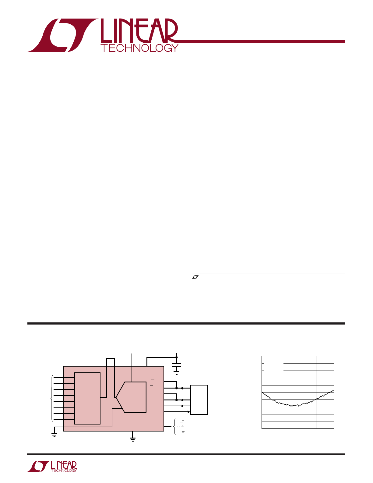
TYPICAL APPLICATIO
7 4 3 2, 8
9
CH0
10
CH1
11
CH2
12
CH3
CH4*
CH5*
CH6*
CH7*
6 COM
4-/8-CHANNEL
MUX
1, 5, 16, 18, 22, 27, 28
13
14
15
17
*THESE PINS ARE NO CONNECTS ON THE LTC2404
–0.12V
ANALOG
INPUTS
REF
1.12V
TO
REF
U
0.1V TO V
V
ADCINMUXOUT
24-BIT
+
∆∑ ADC
–
LTC2404/LTC2408
GND
CC
REFVCC
CSADC
CSMUX
SCK
CLK
D
SDO
2404/08 TA01
IN
F
O
2.7V TO 5.5V
23
20
19
25
21
24
26
1µF
SERIAL DATA LINK
MICROWIRE AND
SPI COMPATABLE
MPU
V
CC
= INTERNAL OSC/50Hz REJECTION
= EXTERNAL CLOCK SOURCE
= INTERNAL OSC/60Hz REJECTION
Total Unadjusted Error vs Output Code
10
VDD = 5V
8
= 5V
V
REF
= 25°C
T
A
6
= LOW
F
O
4
2
0
–2
–4
LINEARITY ERROR (ppm)
–6
–8
–10
0 8,338,608 16,777,215
OUTPUT CODE (DECIMAL)
2404/08 TA02
1
LTC2404/LTC2408
WW
W
U
ABSOLUTE MAXIMUM RATINGS
(Notes 1, 2)
Supply Voltage (VCC) to GND.......................– 0.3V to 7V
Analog Input Voltage to GND ....... –0.3V to (VCC + 0.3V)
Reference Input Voltage to GND .. –0.3V to (VCC + 0.3V)
Digital Input Voltage to GND........ –0.3V to (VCC + 0.3V)
Digital Output Voltage to GND ..... –0.3V to (VCC + 0.3V)
U
W
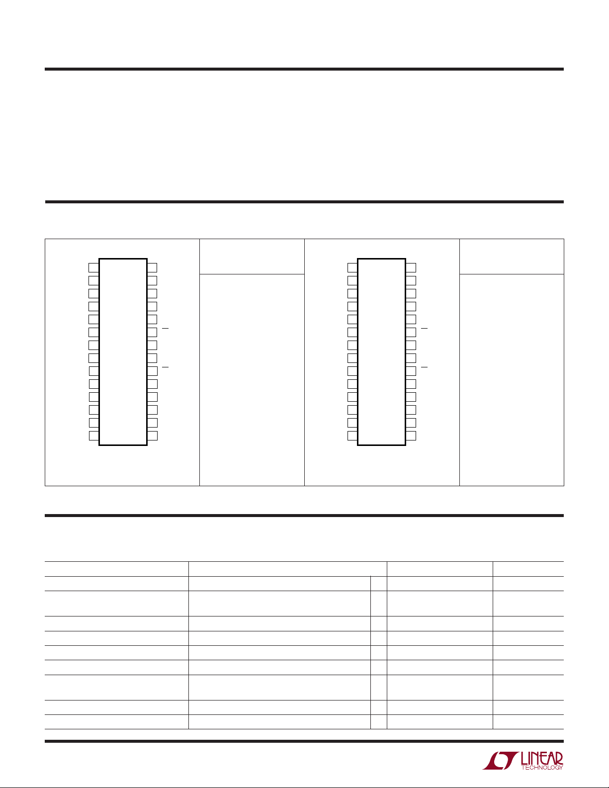
PACKAGE/ORDER INFORMATION
ORDER
PART NUMBER
LTC2404CG
LTC2404IG
GND
V
V
REF
ADCIN
GND
COM
MUXOUT
V
CH0
CH1
CH2
CH3
NC
NC
TOP VIEW
1
2
CC
3
4
5
6
7
8
CC
9
10
11
12
13
14
28
27
26
25
24
23
22
21
20
19
18
17
16
15
GND
GND
F
O
SCK
SDO
CSADC
GND
D
IN
CSMUX
CLK
GND
NC
GND
NC
Operating Temperature Range
LTC2404C/LTC2408C ..............................0°C to 70°C
LTC2404I/LTC2408I ........................... – 40°C to 85°C
Storage Temperature Range ................. –65°C to 150°C
Lead Temperature (Soldering, 10 sec).................. 300°C
U
ORDER
PART NUMBER
LTC2408CG
LTC2408IG
GND
V
V
REF
ADCIN
GND
COM
MUXOUT
V
CH0
CH1
CH2
CH3
CH4
CH5
TOP VIEW
1
2
CC
3
4
5
6
7
8
CC
9
10
11
12
13
14
28
27
26
25
24
23
22
21
20
19
18
17
16
15
GND
GND
F
O
SCK
SDO
CSADC
GND
D
IN
CSMUX
CLK
GND
CH7
GND
CH6
G PACKAGE
28-LEAD PLASTIC SSOP
T
= 125°C, θJA = 130°C/W
JMAX
G PACKAGE
28-LEAD PLASTIC SSOP
T
= 125°C, θJA = 130°C/W
JMAX
Consult factory for Military grade parts.
U
CONVERTER CHARACTERISTICS
temperature range, otherwise specifications are at TA = 25°C. (Notes 3, 4)
PARAMETER CONDITIONS MIN TYP MAX UNITS
Resolution (No Missing Codes) 2.5V ≤ V
Integral Nonlinearity V
REF
V
REF
Offset Error 2.5V ≤ V
Offset Error Drift 2.5V ≤ V
Full-Scale Error 2.5V ≤ V
Full-Scale Error Drift 2.5V ≤ V
Total Unadjusted Error V
REF
V
REF
Output Noise VIN = 0V (Note 13) 1.5 µV
Normal Mode Rejection 60Hz ±2% (Note 7) ● 110 130 dB
≤ VCC, (Note 5) ● 24 Bits
REF
= 2.5V (Note 6) ● 2 10 ppm of V
= 5V (Note 6) ● 4 15 ppm of V
≤ V
REF
≤ V
REF
≤ V
REF
≤ V
REF
= 2.5V 5 ppm of V
= 5V 10 ppm of V
The ● denotes specifications which apply over the full operating
CC
CC
CC
CC
● 0.5 2 ppm of V
0.01 ppm of V
● 4 10 ppm of V
0.02 ppm of V
REF
REF
REF
REF
REF
/°C
REF
/°C
REF
REF
RMS
2
LTC2404/LTC2408
U
CONVERTER CHARACTERISTICS
temperature range, otherwise specifications are at TA = 25°C. (Notes 3, 4)
PARAMETER CONDITIONS MIN TYP MAX UNITS
Normal Mode Rejection 50Hz ±2% (Note 8) ● 110 130 dB
Power Supply Rejection DC V
Power Supply Rejection 60Hz ±2% V
Power Supply Rejection 50Hz ±2% V
= 2.5V, VIN = 0V 100 dB
REF
= 2.5V, VIN = 0V, (Note 7) 110 dB
REF
= 2.5V, VIN = 0V, (Note 8) 110 dB
REF
The ● denotes specifications which apply over the full operating
UU
U
A ALOG I PUT A D REFERE CE
U
The ● denotes specifications which apply over the full operating
temperature range, otherwise specifications are at TA = 25°C. (Note 3)
SYMBOL PARAMETER CONDITIONS MIN TYP MAX UNITS
V
IN
V
REF
C
S(IN)
C
S(REF)
I
IN(LEAK)
I
REF(LEAK)
I
IN(MUX)
R
ON
I
S(OFF)
I
D(OFF)
t
OPEN
t
ON
t
OFF
QIRR MUX Off Isolation VIN = 2V
QINJ Charge Injection RS = 0Ω, CL = 1000pF, VS = 1V ±1pC
C
S(OFF)
C
D(OFF)
Input Voltage Range (Note 14) ● –0.125 • V
Reference Voltage Range ● 0.1 V
Input Sampling Capacitance 10 pF
Reference Sampling Capacitance 15 pF
Input Leakage Current CS = V
Reference Leakage Current V
On Channel Leakage Current VS = 2.5V (Note 15) ● ±20 nA
MUX On-Resistance I
MUX ∆RON vs Temperature 0.5 %/°C
∆RON vs VS (Note 15) 20 %
MUX Off Input Leakage Channel Off, VS = 2.5V ● ±20 nA
MUX Off Output Leakage Channel Off, VD = 2.5V ● ±20 nA
MUX Break-Before-Make Interval 125 290 ns
Enable Turn-On Time VS = 1.5V, RL = 3.4k, CL = 15pF 490 ns
Enable Turn-Off Time VS = 1.5V, RL = 3.4k, CL = 15pF 190 ns
Input Off Capacitance (MUX) 10 pF
Output Off Capacitance (MUX) 10 pF
CC
= 2.5V, CS = V
REF
= 1mA, VCC = 2.7V ● 250 300 Ω
OUT
= 1mA, VCC = 5V ● 120 250 Ω
I
OUT
P-P
CC
, RL = 1k, f = 100kHz 70 dB
● –10 1 10 nA
● –12 1 12 nA
REF
1.125 • V
CC
REF
V
V
3

LTC2404/LTC2408
UU
DIGITAL I PUTS A D DIGITAL OUTPUTS
operating temperature range, otherwise specifications are at TA = 25°C. (Note 3)
SYMBOL PARAMETER CONDITIONS MIN TYP MAX UNITS
V
IH
V
IL
V
IH
V
IL
I
IN
I
IN
C
IN
C
IN
V
OH
V
OL
V
OH
V
OL
I
OZ
VIN H
VIN L
MUX
MUX
High Level Input Voltage 2.7V ≤ VCC ≤ 5.5V ● 2.5 V
CS, F
O
Low Level Input Voltage 4.5V ≤ VCC ≤ 5.5V ● 0.8 V
CS, F
O
High Level Input Voltage 2.7V ≤ VCC ≤ 5.5V (Note 9) ● 2.5 V
SCK 2.7V ≤ V
Low Level Input Voltage 4.5V ≤ VCC ≤ 5.5V (Note 9) ● 0.8 V
SCK 2.7V ≤ V
Digital Input Current 0V ≤ VIN ≤ V
CS, F
O
Digital Input Current 0V ≤ VIN ≤ VCC (Note 9) ● –10 10 µA
SCK
Digital Input Capacitance 10 pF
CS, F
O
Digital Input Capacitance (Note 9) 10 pF
SCK
High Level Output Voltage IO = –800µA ● VCC – 0.5V V
SDO
Low Level Output Voltage IO = 1.6mA ● 0.4V V
SDO
High Level Output Voltage IO = –800µA (Note 10) ● VCC – 0.5V V
SCK
Low Level Output Voltage IO = 1.6mA (Note 10) ● 0.4V V
SCK
High-Z Output Leakage ● –10 10 µA
SDO
MUX High Level Input Voltage V+ = 3V ● 2V
MUX Low Level Input Voltage V+ = 2.4V ● 0.8 V
2.7V ≤ VCC ≤ 3.3V 2.0 V
2.7V ≤ VCC ≤ 5.5V 0.6 V
≤ 3.3V (Note 9) 2.0 V
CC
≤ 5.5V (Note 9) 0.6 V
CC
CC
The ● denotes specifications which apply over the full
● –10 10 µA
WU
POWER REQUIRE E TS
otherwise specifications are at TA = 25°C. (Note 3)
SYMBOL PARAMETER CONDITIONS MIN TYP MAX UNITS
V
CC
I
CC
I
CC(MUX)
Supply Voltage ● 2.7 5.5 V
Supply Current
Conversion Mode CS = 0V (Note 12)
Sleep Mode CS = V
Multiplexer Supply Current All Logic Inputs Tied Together ● 15 40 µA
The ● denotes specifications which apply over the full operating temperature range,
● 200 300 µA
(Note 12) ● 20 30 µA
CC
= 0V or 5V
V
IN
4
LTC2404/LTC2408
UW
TI I G CHARACTERISTICS
otherwise specifications are at TA = 25°C. (Note 3)
SYMBOL PARAMETER CONDITIONS MIN TYP MAX UNITS
f
EOSC
t
HEO
t
LEO
t
CONV
f
ISCK
D
ISCK
f
ESCK
t
LESCK
t
HESCK
t
DOUT_ISCK
t
DOUT_ESCK
t
1
t
2
t
3
t
4
t
KQMAX
t
KQMIN
t
5
t
6
External Oscillator Frequency Range ● 2.56 307.2 kHz
External Oscillator High Period ● 0.5 390 µs
External Oscillator Low Period ● 0.5 390 µs
Conversion Time FO = 0V ● 130.66 133.33 136 ms
Internal SCK Frequency Internal Oscillator (Note 10) 19.2 kHz
Internal SCK Duty Cycle (Note 10) 45 55 %
External SCK Frequency Range (Note 9) ● 2000 kHz
External SCK Low Period (Note 9) ● 250 ns
External SCK High Period (Note 9) ● 250 ns
Internal SCK 32-Bit Data Output Time Internal Oscillator (Notes 10, 12) ● 1.64 1.67 1.70 ms
External SCK 32-Bit Data Output Time (Note 9) ● 32/f
CS ↓ to SDO Low Z ● 0 150 ns
CS ↑ to SDO High Z ● 0 150 ns
CS ↓ to SCK ↓ (Note 10) ● 0 150 ns
CS ↓ to SCK ↑ (Note 9) ● 50 ns
SCK ↓ to SDO Valid ● 200 ns
SDO Hold After SCK ↓ (Note 5) ● 15 ns
SCK Set-Up Before CS ↓ ● 50 ns
SCK Hold After CS ↓ ● 50 ns
The ● denotes specifications which apply over the full operating temperature range,
= V
F
O
CC
External Oscillator (Note 11)
External Oscillator (Notes 10, 11) f
External Oscillator (Notes 10, 11)
● 156.80 160 163.20 ms
● 20480/f
● 256/f
(in kHz) ms
EOSC
/8 kHz
EOSC
(in kHz) ms
EOSC
(in kHz) ms
ESCK
Note 1: Absolute Maximum Ratings are those values beyond which the
life of the device may be impaired.
Note 2: All voltage values are with respect to GND.
Note 3: V
= 2.7 to 5.5V unless otherwise specified, source input
CC
is 0Ω.
Note 4: Internal Conversion Clock source with the F
to GND or to V
= 153600Hz unless otherwise specified.
f
EOSC
or to external conversion clock source with
CC
pin tied
O
Note 5: Guaranteed by design, not subject to test.
Note 6: Integral nonlinearity is defined as the deviation of a code from
a straight line passing through the actual endpoints of the transfer
curve. The deviation is measured from the center of the quantization
band.
Note 7: FO = 0V (internal oscillator) or f
= 153600Hz ±2%
EOSC
(external oscillator).
Note 8: F
= VCC (internal oscillator) or f
O
= 128000Hz ±2%
EOSC
(external oscillator).
Note 9: The converter is in external SCK mode of operation such that
the SCK pin is used as digital input. The frequency of the clock signal
driving SCK during the data output is f
and is expressed in kHz.
ESCK
Note 10: The converter is in internal SCK mode of operation such that
the SCK pin is used as digital output. In this mode of operation the
SCK pin has a total equivalent load capacitance C
Note 11: The external oscillator is connected to the F
oscillator frequency, f
, is expressed in kHz.
EOSC
= 20pF.
LOAD
pin. The external
O
Note 12: The converter uses the internal oscillator.
F
= 0V or FO = VCC.
O
Note 13: The output noise includes the contribution of the internal
calibration operations.
Note 14: For reference voltage values V
of –0.125 • V
to 1.125 • V
REF
is limited by the absolute maximum
REF
rating of the Analog Input Voltage pin (Pin 3). For 2.5V < V
0.267V + 0.89 • V
For 0.267V + 0.89 • V
+ 0.3V.
to V
CC
the input voltage range is –0.3V to 1.125 • V
CC
< V
CC
≤ VCC the input voltage range is –0.3V
REF
> 2.5V the extended input
REF
REF
≤
REF
Note 15: VS is the voltage applied to a channel input. VD is the voltage
applied to the MUX output.
.
5
LTC2404/LTC2408
UW
TYPICAL PERFOR A CE CHARACTERISTICS
Total Unadjusted Error
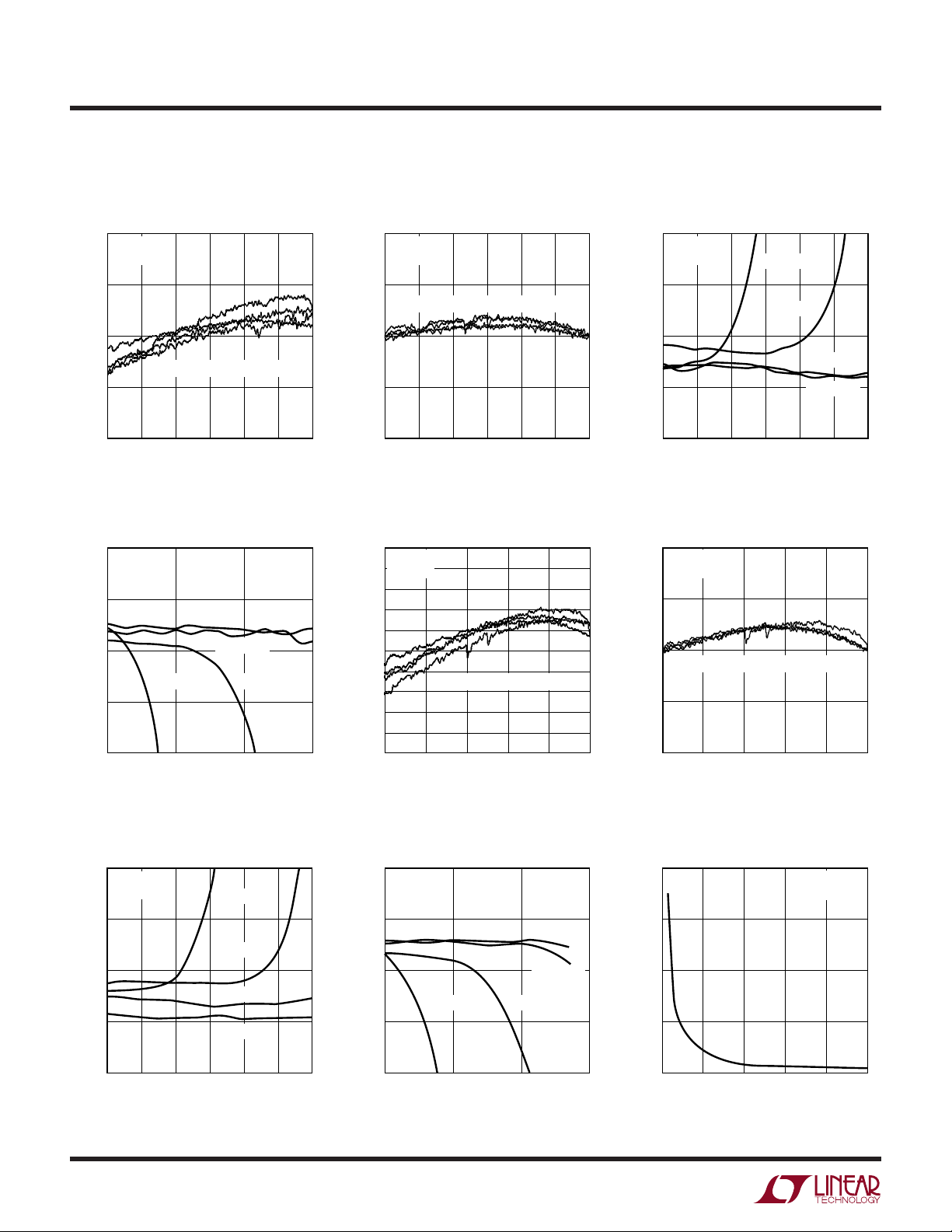
(3V Supply) INL (3V Supply)
10
VCC = 3V
= 3V
V
REF
5
0
ERROR (ppm)
–5
–10
0
TA = –55°C, –45°C, 25°C, 90°C
0.5 1.0 1.5 2.0
INPUT VOLTAGE (V)
Positive Extended Input Range
Total Unadjusted Error (3V Supply)
10
= 3V
V
CC
= 3V
V
REF
5
= –55°C
T
A
0
ERROR (ppm)
–5
–10
3.0
TA = 90°C TA = 25°C
3.1 3.2
INPUT VOLTAGE (V)
TA = –45°C
2.5 3.0
24048 G01
3.3
24048 G04
10
VCC = 3V
V
REF
5
0
ERROR (ppm)
–5
–10
0
Total Unadjusted Error
(5V Supply)
10
VCC = 5V
8
= 5V
V
REF
6
4
2
0
–2
ERROR (ppm)
–4
–6
–8
–10
0
= 3V
TA = –55°C, –45°C, 25°C, 90°C
0.5 1.0 1.5 2.0
INPUT VOLTAGE (V)
TA = –55°C, –45°C, 25°C, 90°C
1
INPUT VOLTAGE (V)
3
2
2.5 3.0
24048 G02
4
24048 G05
5
Negative Extended Input Range
Total Unadjusted Error (3V Supply)
10
VCC = 3V
= 3V
V
REF
5
0
ERROR (ppm)
–5
–10
–0.050
TA = 90°C
TA = 25°C
TA = –45°C
TA = –55°C
INPUT VOLTAGE (V)
INL (5V Supply)
10
VCC = 5V
= 5V
V
REF
5
0
ERROR (ppm)
–5
–10
TA = –55°C, –45°C, 25°C, 90°C
1
0
2
INPUT VOLTAGE (V)
3
–0.30
–0.25–0.20–0.15–0.10
24048 G03
4
5
24048 G06
Negative Extended Input Range
Total Unadjusted Error (5V Supply) Offset Error vs Reference Voltage
10
VCC = 5V
= 5V
V
REF
5
0
ERROR (ppm)
–5
–10
–0.050
INPUT VOLTAGE (V)
TA = 90°C
TA = 25°C
TA = –45°C
TA = –55°C
–0.30
–0.25–0.20–0.15–0.10
24048 G07
Positive Extended Input Range
Total Unadjusted Error (5V Supply)
10
V
= 5V
CC
= 5V
V
REF
5
0
ERROR (ppm)
–5
–10
5.0
TA = 90°C TA = 25°C
5.1 5.2
INPUT VOLTAGE (V)
T
TA = –45°C
= –55°C
A
24048 G08
5.3
20
)
15
REF
10
5
RMS NOISE (ppm OF V
0
1
0
REFERENCE VOLTAGE (V)
3
2
6
VCC = 5V
T
= 25°C
A
4
24048 G10
5
UW
V
CC
2.7
RMS NOISE (ppm)
0
2.5
5.0
3.2 3.7 4.2 4.7
24048 G12
5.2
V
REF
= 2.5V
T
A
= 25°C
TEMPERATURE (°C)
–50
–5.0
OFFSET ERROR (ppm)
–2.5
0
2.5
5.0
–25 0 25 50
24048 G15
75 100 125
VCC = 5V
V
REF
= 5V
V
IN
= 0V
V
CC
2.7
0
FULL-SCALE ERROR (ppm)
2
1
3
5
4
6
3.2 3.7 4.2 4.7
24048 G18
5.2
V
REF
= 2.5V
V
IN
= 2.5V
T
A
= 25°C
TYPICAL PERFOR A CE CHARACTERISTICS
LTC2404/LTC2408
RMS Noise vs Reference Voltage Offset Error vs V
20
)
15
REF
10
5
RMS NOISE (ppm OF V
0
1
0
REFERENCE VOLTAGE (V)
VCC = 5V
T
= 25°C
A
3
4
2
5
24048 G10
5.0
V
REF
T
= 25°C
A
2.5
0
OFFSET ERROR (ppm)
–2.5
–5.0
2.7
RMS Noise vs CODE OUT
1500
1000
V
= 5V
CC
= 5V
V
REF
= 0V
V
IN
1.00
0.75
0.50
VCC = 5V
V
REF
= –0.3V TO 5.3V
V
IN
= 25°C
T
A
CC
= 2.5V
3.2 3.7 4.2 4.7
= 5V
V
CC
5.2
24048 G11
RMS Noise vs V
Offset Error vs TemperatureNoise Histogram
CC
500
NUMBER OF READINGS
0
5.0
2.5
0
–2.5
FULL-SCALE ERROR (ppm)
–5.0
–0.5 0 0.5 1.0
OUTPUT CODE (ppm)
Full-Scale Error vs Temperature
VCC = 5V
V
REF
= 5V
V
IN
–50
–25 0 25 50
TEMPERATURE (°C)
75 100 125
24048 G13
= 5V
24048 G16
RMS NOISE (ppm)
0.25
1.5–1.0
0
0
7FFFFF
CODE OUT (HEX)
FFFFFF
24048 G14
Full-Scale Error
vs Reference Voltage
10.0
7.5
5.0
2.5
FULL-SCALE ERROR (ppm)
0
1
0
REFERENCE VOLTAGE (V)
VCC = 5V
= V
V
IN
REF
3
4
2
5
24048 G17
Full-Scale Error vs V
CC
7
LTC2404/LTC2408
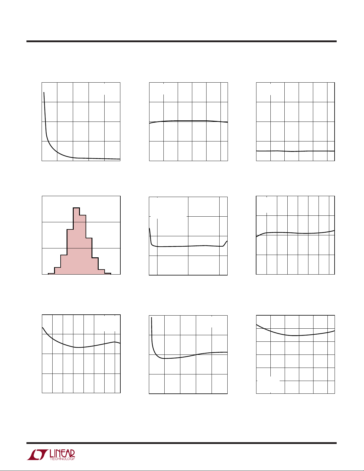
INPUT FREQUENCY
0
–60
–40
0
24048 F23
–80
–100
fS/2 f
S
–120
–140
–20
REJECTION (dB)
UW
TYPICAL PERFOR A CE CHARACTERISTICS
Conversion Current vs Temperature
230
220
210
200
190
180
SUPPLY CURRENT (µA)
170
160
150
–50
PSRR vs Frequency at V
–10
VCC = 4.1V
V
IN
–30
= 25°C
T
A
= 0
F
0
–50
–70
VCC = 5.5V
VCC = 4.1V
VCC= 2.7V
–25 0 50
= 0V
25
TEMPERATURE (°C)
75 100 125
CC
24048 G19
Sleep Current vs Temperature
30
25
20
15
10
SUPPLY CURRENT (µA)
5
0
–50
–25 0
VCC = 5.5V
V
CC
50 100 125
25 75
TEMPERATURE (°C)
PSRR vs Frequency at V
0
VCC = 4.1V
= 0V
V
IN
–20
= 25°C
T
A
= 0
F
O
–40
–60
= 2.7V
CC
24048 G20
PSRR vs Frequency at V
0
VCC = 4.1V
= 0V
V
IN
–20
= 25°C
T
A
= 0
F
O
–40
–60
REJECTION (dB)
–80
–100
–120
1
15,360Hz 153,600Hz
100 10k 1M
FREQUENCY AT VCC (Hz)
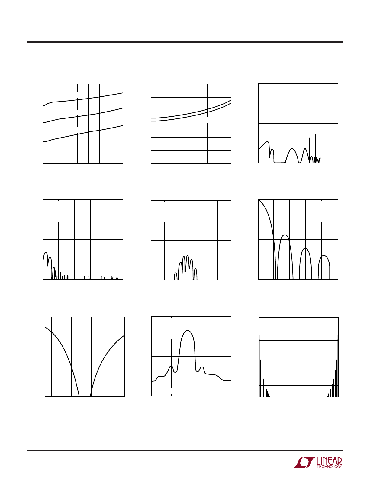
Rejection vs Frequency at V
0
–20
–40
–60
CC
VCC = 5V
V
REF
V
IN
F
O
24048 G21
IN
= 5V
= 2.5V
= 0
REJECTION (dB)
REJECTION (dB)
–90
–110
–130
0
50 100 150 200
FREQUENCY AT V
(Hz)
CC
Rejection vs Frequency at V
–60
–70
–80
–90
–100
–110
–120
–130
–140
–12–8–404812
INPUT FREQUENCY DEVIATION FROM NOTCH FREQUENCY (%)
250
24048 G22
IN
24048 G25
REJECTION (dB)
–80
–100
–120
15200
15300 15350 15400
15250
FREQUENCY AT VCC (Hz)
Rejection vs Frequency at V
0
VCC = 5V
= 5V
V
REF
–20
= 2.5V
V
IN
= 0
F
O
–40
–60
REJECTION (dB)
–80
–100
–120
SAMPLE RATE = 15.36kHz ±2%
15100
15200 15300 15400 15500
FREQUENCY AT VIN (Hz)
15450 15500
24048 G23
IN
24048 G26
REJECTION (dB)
–80
–100
–120
1
50 100 150 200
FREQUENCY AT VIN (Hz)
Rejection vs Frequency at V
250
24048 G24
IN
8
UW
TYPICAL PERFOR A CE CHARACTERISTICS
INL vs Maximum Output Rate
24
22
20
18
16
INL (BITS)
14
12
10
8
0
VCC = 5V
V
= 5V
REF
F
= EXTERNAL
0
(20480 × MAXIMUM
OUTPUT RATE)
TA = 25°C
T
= 90°C
A
15 20 25105 303540455055
MAXIMUM OUTPUT RATE (Hz)
60
24048 G27
24
22
20
18
16
14
RESOLUTION (BITS)*
12
10
8
LTC2404/LTC2408
Resolution vs Maximum
Output Rate
FO = EXTERNAL
(20480 × MAXIMUM
OUTPUT RATE)
T
T
VCC = V
VCC = V
= 3V
REF
/RMS NOISE)
LOG(V
*RESOLUTION =
0
15 20 25105 303540455055
MAXIMUM OUTPUT RATE (Hz)
REF
LOG (2)
= 25°C
A
= 90°C
A
REF
= 5V
60
24048 G28
U
UU
PIN FUNCTIONS
GND (Pins 1, 5, 16, 18, 22, 27, 28): Ground. Should be
connected directly to a ground plane through a minimum
length trace or it should be the single-point-ground in a
single point grounding system.
VCC (Pins 2, 8): Positive Supply Voltage. 2.7V ≤ VCC ≤
5.5V. Bypass to GND with a 10µF tantalum capacitor in
parallel with 0.1µF ceramic capacitor as close to the part
as possible.
V
(Pin 3): Reference Input. The reference voltage range
REF
is 0.1V to VCC.
ADCIN (Pin 4): Analog Input. The input voltage range is
–0.125 • V
voltage range may be limited by the pin absolute maximum rating of –0.3V to VCC + 0.3V.
COM (Pin 6): Signal Ground. Should be connected directly
to a ground plane through minimum length trace.
MUXOUT (Pin 7): MUX Output. This pin is the output of the
multiplexer. Tie to ADCIN for normal operation.
CH0 (Pin 9): Analog Multiplexer Input.
to 1.125 • V
REF
REF
. For V
> 2.5V the input
REF
CH4 (Pin 13): Analog Multiplexer Input. No connect on the
LTC2404.
CH5 (Pin 14): Analog Multiplexer Input. No connect on the
LTC2404.
CH6 (Pin 15): Analog Multiplexer Input. No connect on the
LTC2404.
CH7 (Pin 17): Analog Multiplexer Input. No connect on the
LTC2404.
CLK (Pin 19): Shift Clock for Data In. This clock synchronizes the serial data transfer into the MUX. For normal
operation, drive this pin in parallel with SCK.
CSMUX (Pin 20): MUX Chip Select Input. A logic high on
this input allows the MUX to receive a channel address. A
logic low enables the selected MUX channel and connects
it to the MUXOUT pin for A/D conversion. For normal
operation, drive this pin in parallel with CSADC.
DIN (Pin 21): Digital Data Input. The multiplexer address
is shifted into this input on the last four rising CLK edges
before CSMUX goes low.
CH1 (Pin 10): Analog Multiplexer Input.
CH2 (Pin 11): Analog Multiplexer Input.
CH3 (Pin 12): Analog Multiplexer Input.
CSADC (Pin 23): ADC Chip Select Input. A low on this pin
enables the SDO digital output and following each conversion, the ADC automatically enters the Sleep mode and
remains in this low power state as long as CSADC is high.
9
LTC2404/LTC2408
3.4k
SDO
24048 TC02
HI-Z TO V
OL
VOH TO V
OL
VOL TO HI-Z
C
LOAD
= 20pF
V
CC
U
UU
PIN FUNCTIONS
A high on this pin also disables the SDO digital output. A
low-to-high transition on CSADC during the Data Output
state aborts the data transfer and starts a new conversion.
For normal operation, drive this pin in parallel with CSMUX.
SDO (Pin 24): Three-State Digital Output. During the data
output period this pin is used for serial data output. When
the chip select CSADC is high (CSADC = VCC), the SDO pin
is in a high impedance state. During the Conversion and
Sleep periods, this pin can be used as a conversion status
output. The conversion status can be observed by pulling
CSADC low.
SCK (Pin 25): Shift Clock for Data Out. This clock synchronizes the serial data transfer of the ADC data output. Data
UU
W
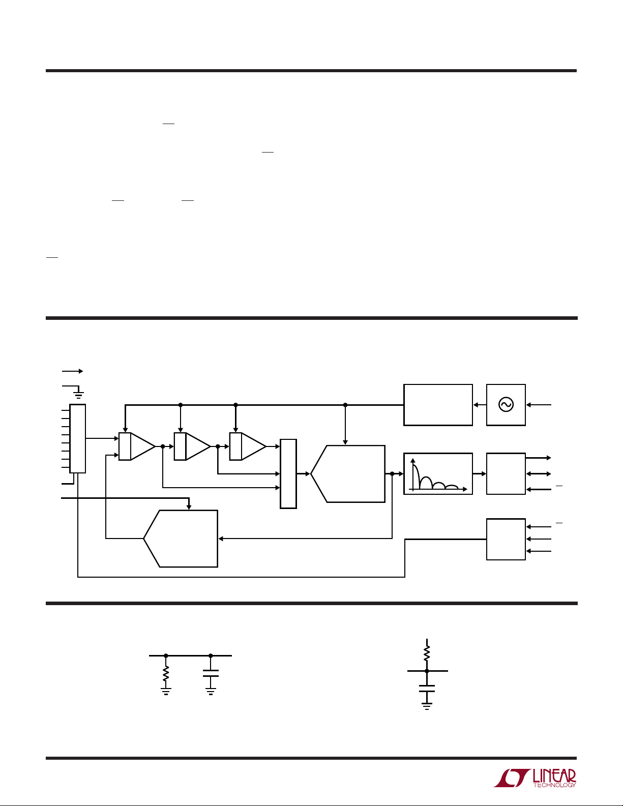
FU CTIO AL BLOCK DIAGRA
V
CC
GND
CH0
CH1
CH2
CH3
CH4
CH5
CH6
CH7
COM
V
REF
8-CHANNEL MUX
∫∫∫
∑
is shifted out of SDO on the falling edge of SCK. For normal
operation, drive this pin in parallel with CLK.
FO (Pin 26): Digital input which controls the ADC’s notch
frequencies and conversion time. When the FO pin is
connected to VCC (FO = VCC), the converter uses its internal
oscillator and the digital filter first null is located at 50Hz.
When the FO pin is connected to GND (FO = OV), the
converter uses its internal oscillator and the digital filter
first null is located at 60Hz. When FO is driven by an
external clock signal with a frequency f
, the converter
EOSC
uses this signal as its clock and the digital filter first null is
located at a frequency f
word rate is f
ADC
EOSC
/20480.
AUTOCALIBRATION
AND CONTROL
DECIMATING FIR
/2560. The resulting output
EOSC
INTERNAL
OSCILLATOR
(INT/EXT)
SERIAL
INTERFACE
F
O
SDO
SCK
CSADC
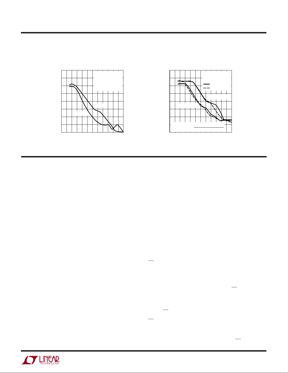
TEST CIRCUITS
10
SDO
DAC
3.4k
HI-Z TO V
VOL TO V
OH
VOH TO HI-Z
24048 BD
CSMUX
D
IN
CLK
CHANNEL
SELECT
= 20pF
C
LOAD
OH
24048 TC01
LTC2404/LTC2408
U
WUU
APPLICATIONS INFORMATION
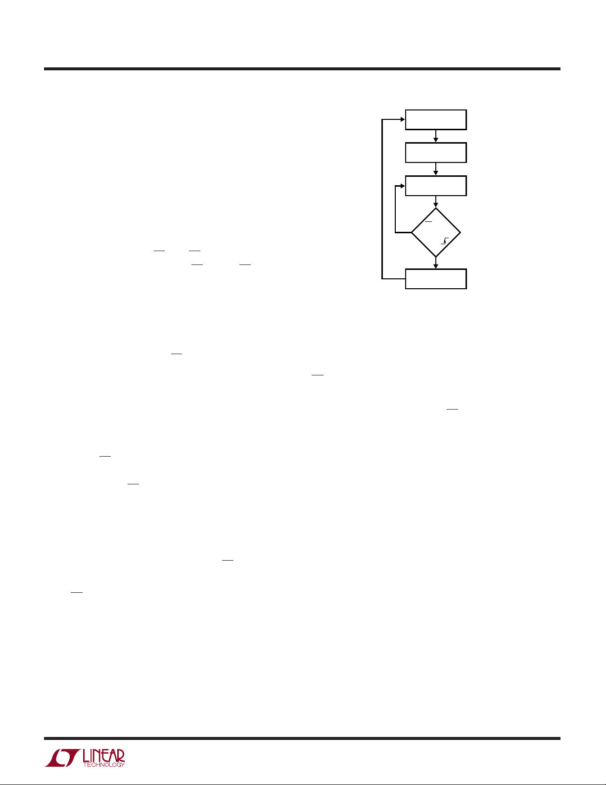
Converter Operation Cycle
The LTC2404/LTC2408 are low power, 4-/8-channel deltasigma analog-to-digital converters with easy-to-use
4-wire interfaces. Their operation is simple and made up
of four states. The converter operation begins with the
conversion, followed by a low power sleep state and
concluded with the data output (see Figure 1). Channel
selection may be performed while the device is in the sleep
state or at the conclusion of the data output state. The
interface consists of serial data output (SDO), serial clock
(CLK/SCK), chip select (CSADC/CSMUX) and data input
(DIN). By tying SCK to CLK and CSADC to CSMUX, the
interface requires only four wires.
Initially, the LTC2404 or LTC2408 performs a conversion.
Once the conversion is complete, the device enters the
sleep state. While in the sleep state, power consumption
is reduced by an order of magnitude. The part remains in
the sleep state as long as CSADC is logic HIGH. The
conversion result is held indefinitely in a static shift
register while the converter is in the sleep state.
Channel selection for the next conversion cycle is performed while the device is in the sleep state or at the end
of the data output state. A specific channel is selected by
applying a 4-bit serial word to the DIN pin on the rising edge
of CLK while CSMUX is HIGH, see Figure 3 and Table 3. The
channel is selected based on the last four bits clocked into
the DIN pin before CSMUX goes low. If DIN is all 0’s, the
previous channel remains selected.
CONVERT
CHANNEL SELECT
(SLEEP)
SLEEP
CSADC
1
AND
SCK
0
DATA OUTPUT
(CHANNEL SELECT)
Figure 1. LTC2408 State Transition Diagram
24048 F01
edge of SCK, see Figure 3. The data output state is
concluded once 32 bits are read out of the ADC or when
CSADC is brought HIGH. The device automatically initiates
a new conversion and the cycle repeats.
Through timing control of the CSADC and SCK pins, the
LTC2404/LTC2408 offer two modes of operation: internal
or external SCK. These modes do not require programming configuration registers; moreover, they do not disturb the cyclic operation described above. These modes of
operation are described in detail in the Serial Interface
Timing Modes section.
In the example, Figure 3, the MUX channel is selected
during the sleep state, just before the data output state
begins. Once the channel selection is complete, the device
remains in the sleep state as long as CSADC remains
HIGH.
Once CSADC is pulled low, the device begins outputting
the conversion result. There is no latency in the conversion
result. Since there is no latency, the first conversion
following a change in input channel is valid and corresponds to that channel. The data output corresponds to
the conversion just performed. This result is shifted out on
the serial data output pin (SDO) under the control of the
serial clock (SCK). Data is updated on the falling edge of
SCK allowing the user to reliably latch data on the rising
Conversion Clock
A major advantage delta-sigma converters offer over
conventional type converters is an on-chip digital filter
(commonly known as Sinc or Comb filter). For high
resolution, low frequency applications, this filter is typically designed to reject line frequencies of 50 or 60Hz plus
their harmonics. In order to reject these frequencies in
excess of 110dB, a highly accurate conversion clock is
required. The LTC2404/LTC2408 incorporate an on-chip
highly accurate oscillator. This eliminates the need for
external frequency setting components such as crystals or
oscillators. Clocked by the on-chip oscillator, the LTC2404/
LTC2408 reject line frequencies (50 or 60Hz ±2%) a
minimum of 110dB.
11
 Loading...