

Linear Technology LTC2400 Datasheet
FEATURES
■
24-Bit ADC in SO-8 Package
■
4ppm INL, No Missing Codes
■
4ppm Full-Scale Error
■
Single Conversion Settling Time
for Multiplexed Applications
■
0.5ppm Offset
■
0.3ppm Noise
■
Internal Oscillator—No External Components
Required
■
110dB Min, 50Hz/60Hz Notch Filter
■
Reference Input Voltage: 0.1V to V
■
Live Zero—Extended Input Range Accommodates
CC
12.5% Overrange and Underrange
■
Single Supply 2.7V to 5.5V Operation
■
Low Supply Current (200µA) and Auto Shutdown
U
APPLICATIO S
■
Weight Scales
■
Direct Temperature Measurement
■
Gas Analyzers
■
Strain-Gage Transducers
■
Instrumentation
■
Data Acquisition
■
Industrial Process Control
■
6-Digit DVMs
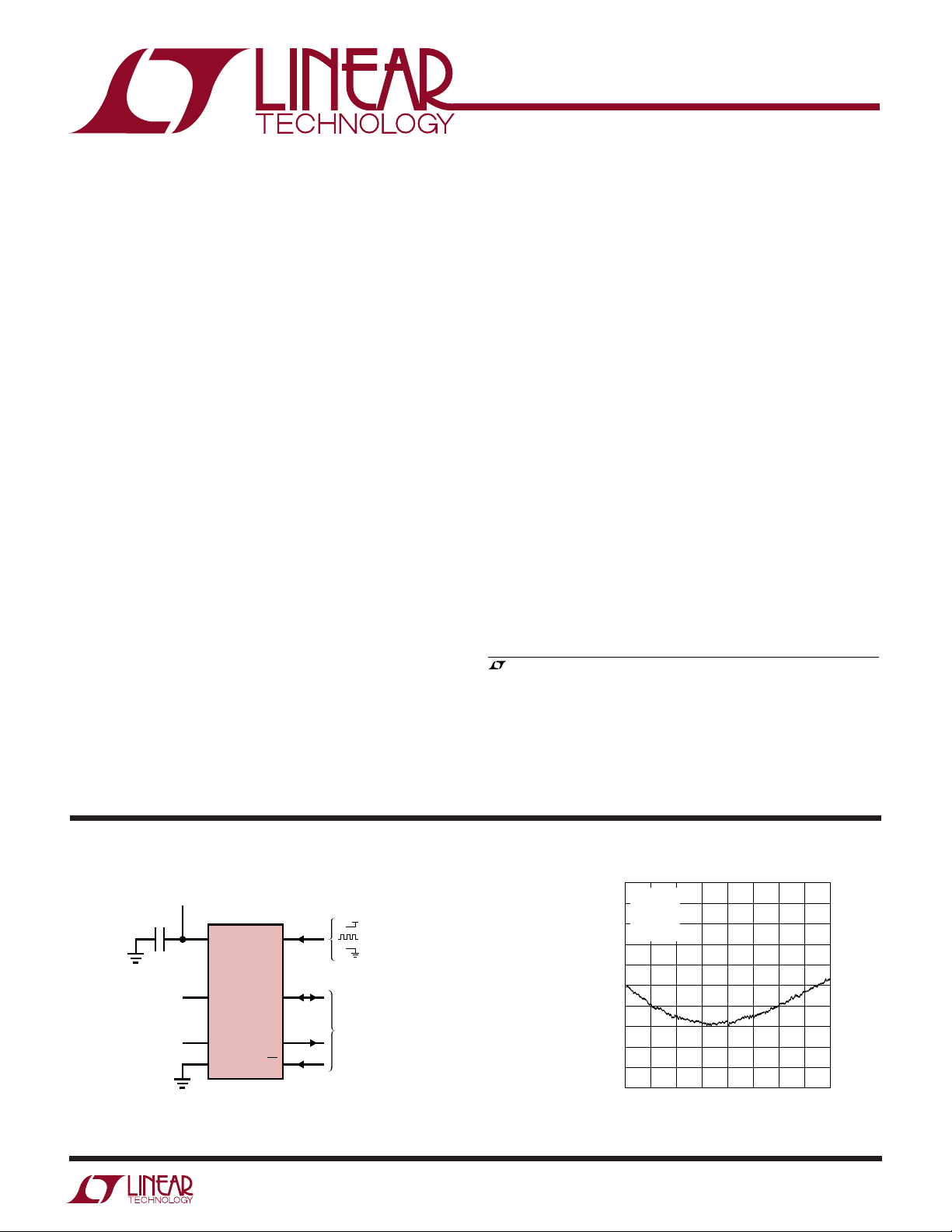
LTC2400
24-Bit µPower
No Latency ∆Σ
TM
ADC in SO-8
U
DESCRIPTIO
The LTC®2400 is a 2.7V to 5.5V micropower 24-bit
converter with an integrated oscillator, 4ppm INL and
0.3ppm RMS noise. It uses delta-sigma technology and
provides single cycle settling time for multiplexed applications. Through a single pin the LTC2400 can be configured for better than 110dB rejection at 50Hz or 60Hz ±2%,
or it can be driven by an external oscillator for a user
defined rejection frequency in the range 1Hz to 120Hz.
The internal oscillator requires no external frequency
setting components.
The converter accepts any external reference voltage from
0.1V to VCC. With its extended input conversion range of
–12.5% V
resolves the offset and overrange problems of preceding
sensors or signal conditioning circuits.
The LTC2400 communicates through a flexible 3-wire
digital interface which is compatible with SPI and
MICROWIRETM protocols.
, LTC and LT are registered trademarks of Linear Technology Corporation.
No Latency ∆Σ is a trademark of Linear Technology Corporation.
MICROWIRE is a trademark of National Semiconductor Corporation.
to 112.5% V
REF
, the LTC2400 smoothly
REF
TYPICAL APPLICATIO
2.7V TO 5.5V
1µF
–0.12V
REFERENCE
VOLTAGE
0.1V TO V
ANALOG
INPUT RANGE
TO 1.12V
REF
REF
CC
V
CC
V
REF
V
IN
GND CS
LTC2400
SCK
SDO
F
O
U
V
CC
= INTERNAL OSC/50Hz REJECTION
= EXTERNAL CLOCK SOURCE
= INTERNAL OSC/60Hz REJECTION
3-WIRE
SPI INTERFACE
2400 TA01
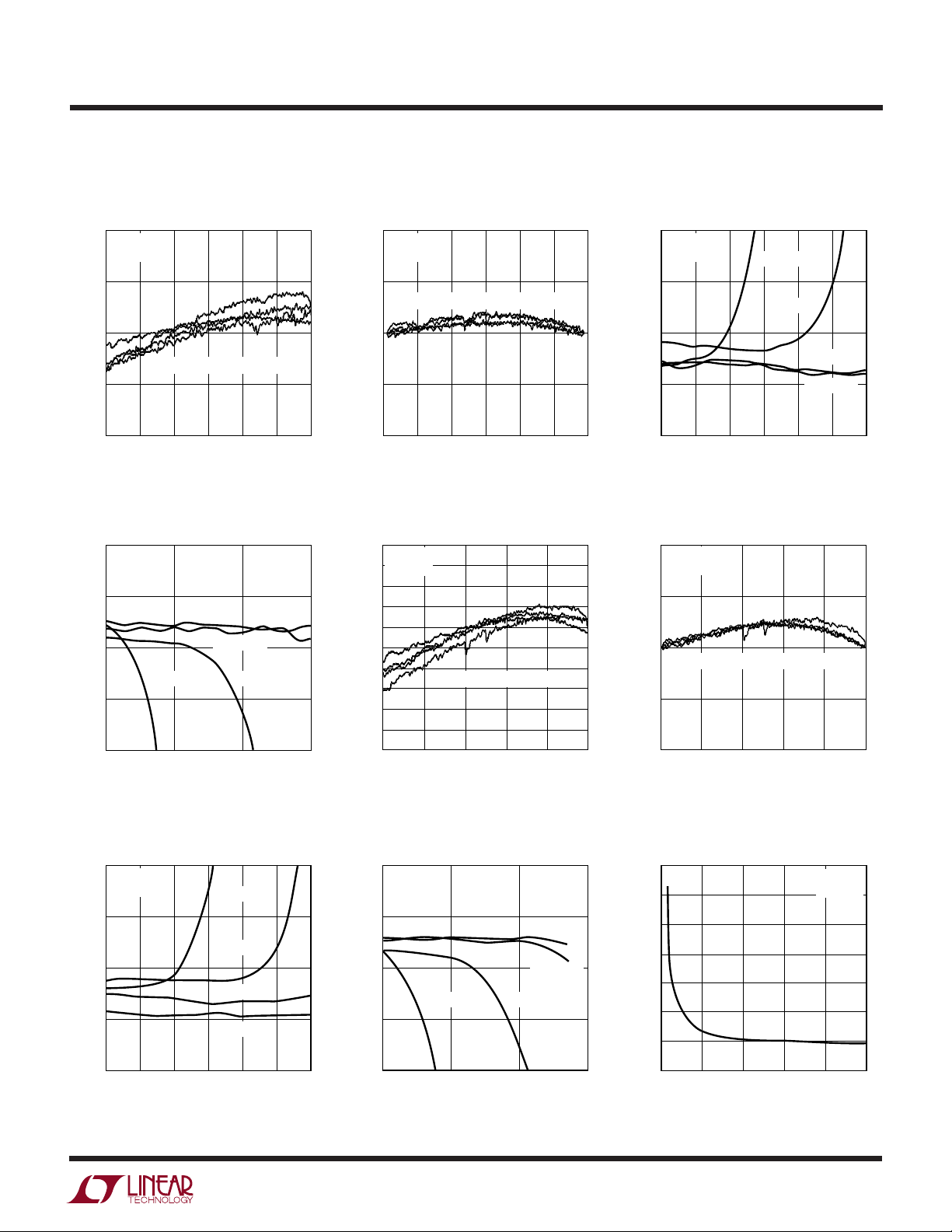
Total Unadjusted Error vs Output Code
10
VCC = 5V
8
= 5V
V
REF
= 25°C
T
A
6
= LOW
F
O
4
2
0
–2
–4
LINEARITY ERROR (ppm)
–6
–8
–10
0 8,338,608 16,777,215
OUTPUT CODE (DECIMAL)
2400 TA02
1
LTC2400
WW
W
ABSOLUTE MAXIMUM RATINGS
U
UUW
PACKAGE/ORDER INFORMATION
(Notes 1, 2)
Supply Voltage (VCC) to GND.......................–0.3V to 7V
Analog Input Voltage to GND ....... –0.3V to (VCC + 0.3V)
Reference Input Voltage to GND .. –0.3V to (VCC + 0.3V)
Digital Input Voltage to GND........ –0.3V to (VCC + 0.3V)
Digital Output Voltage to GND ..... –0.3V to (VCC + 0.3V)
Operating Temperature Range
LTC2400C ............................................... 0°C to 70°C
LTC2400I............................................ – 40°C to 85°C
Storage Temperature Range ................. –65°C to 150°C
TOP VIEW
V
1
CC
V
2
REF
V
3
IN
GND
4
S8 PACKAGE
8-LEAD PLASTIC SO
T
= 125°C, θJA = 130°C/W
JMAX
Consult factory for Military grade parts.
8
F
O
SCK
7
SDO
6
CS
5
ORDER PART NUMBER
LTC2400CS8
LTC2400IS8
S8 PART MARKING
2400
2400I
Lead Temperature (Soldering, 10 sec)..................300°C
U
CONVERTER CHARACTERISTICS
temperature range, otherwise specifications are at TA = 25°C. (Notes 3, 4)
PARAMETER CONDITIONS MIN TYP MAX UNITS
Resolution (No Missing Codes) 0.1V ≤ V
Integral Nonlinearity V
Offset Error 2.5V ≤ V
Offset Error Drift 2.5V ≤ V
Full-Scale Error 2.5V ≤ V
Full-Scale Error Drift 2.5V ≤ V
Total Unadjusted Error V
Output Noise VIN = 0V (Note 13) 1.5 µV
Normal Mode Rejection 60Hz ±2% (Note 7) ● 110 130 dB
Normal Mode Rejection 50Hz ±2% (Note 8) ● 110 130 dB
Power Supply Rejection, DC V
Power Supply Rejection, 60Hz ±2% V
Power Supply Rejection, 50Hz ±2% V
REF
V
REF
REF
V
REF
REF
REF
REF
≤ VCC, (Note 5) ● 24 Bits
REF
= 2.5V (Note 6) ● 2 10 ppm of V
= 5V (Note 6) ● 4 15 ppm of V
≤ V
REF
CC
≤ V
REF
CC
≤ V
REF
CC
≤ V
REF
CC
= 2.5V 5 ppm of V
= 5V 10 ppm of V
= 2.5V, VIN = 0V 100 dB
= 2.5V, VIN = 0V, (Notes 7, 15) 110 dB
= 2.5V, VIN = 0V, (Notes 8, 15) 110 dB
The ● denotes specifications which apply over the full operating
● 0.5 2 ppm of V
0.01 ppm of V
● 4 10 ppm of V
0.02 ppm of V
REF
REF
REF
REF
REF
/°C
REF
/°C
REF
REF
RMS
UU
U
A ALOG I PUT A D REFERE CE
U
The ● denotes specifications which apply over the full operating
temperature range, otherwise specifications are at TA = 25°C. (Note 3)
SYMBOL PARAMETER CONDITIONS MIN TYP MAX UNITS
V
IN
V
REF
C
S(IN)
C
S(REF)
I
IN(LEAK)
I
REF(LEAK)
Input Voltage Range (Note 14) ● –0.125 • V
Reference Voltage Range ● 0.1 V
Input Sampling Capacitance 10 pF
Reference Sampling Capacitance 15 pF
Input Leakage Current CS = V
Reference Leakage Current V
= 2.5V, CS = V
REF
CC
CC
● –10 1 10 nA
● –10 1 10 nA
REF
1.125 • V
CC
REF
2
V
V
LTC2400
UU
DIGITAL I PUTS A D DIGITAL OUTPUTS
operating temperature range, otherwise specifications are at TA = 25°C. (Note 3)
SYMBOL PARAMETER CONDITIONS MIN TYP MAX UNITS
V
IH
V
IL
V
IH
V
IL
I
IN
I
IN
C
IN
C
IN
V
OH
V
OL
V
OH
V
OL
I
OZ
High Level Input Voltage 2.7V ≤ VCC ≤ 5.5V ● 2.5 V
CS, F
O
Low Level Input Voltage 4.5V ≤ VCC ≤ 5.5V ● 0.8 V
CS, F
O
High Level Input Voltage 2.7V ≤ VCC ≤ 5.5V (Note 9) ● 2.5 V
SCK 2.7V ≤ V
Low Level Input Voltage 4.5V ≤ VCC ≤ 5.5V (Note 9) ● 0.8 V
SCK 2.7V ≤ V
Digital Input Current 0V ≤ VIN ≤ V
CS, F
O
Digital Input Current 0V ≤ VIN ≤ VCC (Note 9) ● –10 10 µA
SCK
Digital Input Capacitance 10 pF
CS, F
O
Digital Input Capacitance (Note 9) 10 pF
SCK
High Level Output Voltage IO = –800µA ● VCC – 0.5V V
SDO
Low Level Output Voltage IO = 1.6mA ● 0.4V V
SDO
High Level Output Voltage IO = –800µA (Note 10) ● VCC – 0.5V V
SCK
Low Level Output Voltage IO = 1.6mA (Note 10) ● 0.4V V
SCK
High-Z Output Leakage ● –10 10 µA
SDO
2.7V ≤ VCC ≤ 3.3V 2.0 V
2.7V ≤ VCC ≤ 5.5V 0.6 V
≤ 3.3V (Note 9) 2.0 V
CC
≤ 5.5V (Note 9) 0.6 V
CC
CC
The ● denotes specifications which apply over the full
● –10 10 µA
WU
POWER REQUIRE E TS
otherwise specifications are at TA = 25°C. (Note 3)
SYMBOL PARAMETER CONDITIONS MIN TYP MAX UNITS
V
CC
I
CC
Supply Voltage ● 2.7 5.5 V
Supply Current
Conversion Mode CS = 0V (Note 12)
Sleep Mode CS = V
The ● denotes specifications which apply over the full operating temperature range,
● 200 300 µA
(Note 12) ● 20 30 µA
CC
3
LTC2400
UW
TI I G CHARACTERISTICS
range, otherwise specifications are at TA = 25°C. (Note 3)
SYMBOL PARAMETER CONDITIONS MIN TYP MAX UNITS
f
EOSC
t
HEO
t
LEO
t
CONV
f
ISCK
D
ISCK
f
ESCK
t
LESCK
t
HESCK
t
DOUT_ISCK
t
DOUT_ESCK
t
1
t2 CS ↑ to SDO High Z ● 0 150 ns
t3 CS ↓ to SCK ↓ (Note 10) ● 0 150 ns
t4 CS ↓ to SCK ↑ (Note 9) ● 50 ns
t
KQMAX
t
KQMIN
t
5
t
6
External Oscillator Frequency Range ● 2.56 307.2 kHz
External Oscillator High Period ● 0.5 390 µs
External Oscillator Low Period ● 0.5 390 µs
Conversion Time FO = 0V ● 130.66 133.33 136 ms
Internal SCK Frequency Internal Oscillator (Note 10) 19.2 kHz
Internal SCK Duty Cycle (Note 10) ● 45 55 %
External SCK Frequency Range (Note 9) ● 2000 kHz
External SCK Low Period (Note 9) ● 250 ns
External SCK High Period (Note 9) ● 250 ns
Internal SCK 32-Bit Data Output Time Internal Oscillator (Notes 10, 12) ● 1.64 1.67 1.70 ms
External SCK 32-Bit Data Output Time (Note 9) ● 32/f
CS ↓ to SDO Low Z ● 0 150 ns
SCK ↓ to SDO Valid ● 200 ns
SDO Hold After SCK ↓ (Note 5) ● 15 ns
SCK Set-Up Before CS ↓ ● 50 ns
SCK Hold After CS ↓ ● 50 ns
The ● denotes specifications which apply over the full operating temperature
= V
F
O
CC
External Oscillator (Note 11)
External Oscillator (Notes 10, 11) f
External Oscillator (Notes 10, 11)
● 156.80 160 163.20 ms
● 20480/f
● 256/f
(in kHz) ms
EOSC
/8 kHz
EOSC
(in kHz) ms
EOSC
(in kHz) ms
ESCK
Note 1: Absolute Maximum Ratings are those values beyond which the
life of the device may be impaired.
Note 2: All voltage values are with respect to GND.
Note 3: V
Note 4: Internal Conversion Clock source with the F
to GND or to V
f
EOSC
= 2.7 to 5.5V unless otherwise specified.
CC
or to external conversion clock source with
CC
= 153600Hz unless otherwise specified.
pin tied
O
Note 5: Guaranteed by design, not subject to test.
Note 6: Integral nonlinearity is defined as the deviation of a code from
a straight line passing through the actual endpoints of the transfer
curve. The deviation is measured from the center of the quantization
band.
Note 7: FO = 0V (internal oscillator) or f
= 153600Hz ±2%
EOSC
(external oscillator).
Note 8: F
= VCC (internal oscillator) or f
O
= 128000Hz ±2%
EOSC
(external oscillator).
Note 9: The converter is in external SCK mode of operation such that
the SCK pin is used as digital input. The frequency of the clock signal
driving SCK during the data output is f
and is expressed in kHz.
ESCK
Note 10: The converter is in internal SCK mode of operation such that
the SCK pin is used as digital output. In this mode of operation the
SCK pin has a total equivalent load capacitance C
LOAD
= 20pF.
Note 11: The external oscillator is connected to the FO pin. The external
oscillator frequency, f
, is expressed in kHz.
EOSC
Note 12: The converter uses the internal oscillator.
= 0V or FO = VCC.
F
O
Note 13: The output noise includes the contribution of the internal
calibration operations.
Note 14: For reference voltage values V
of –0.125 • V
to 1.125 • V
REF
is limited by the absolute maximum
REF
rating of the Analog Input Voltage pin (Pin 3). For 2.5V < V
0.267V + 0.89 • V
For 0.267V + 0.89 • V
+ 0.3V.
to V
CC
the input voltage range is –0.3V to 1.125 • V
CC
< V
CC
≤ VCC the input voltage range is –0.3V
REF
> 2.5V the extended input
REF
REF
≤
.
REF
Note 15: The DC voltage at VCC = 4.1V, and the AC voltage applied to
is 2.8V
V
CC
P-P
4
UW
REFERENCE VOLTAGE
0
4
5
6
34
2400 G09
3
2
12 5
1
0
–1
OFFSET ERROR (ppm)
VCC = 5V
T
A
= 25°C
TYPICAL PERFOR A CE CHARACTERISTICS
LTC2400
Total Unadjusted Error
(3V Supply) INL (3V Supply)
10
VCC = 3V
= 3V
V
REF
5
0
ERROR (ppm)
–5
–10
0
TA = –55°C, –45°C, 25°C, 90°C
0.5 1.0 1.5 2.0
INPUT VOLTAGE (V)
Positive Input Extended Total
Unadjusted Error (3V Supply)
10
= 3V
V
CC
= 3V
V
REF
5
= –55°C
T
A
0
ERROR (ppm)
–5
–10
3.0
TA = 90°C TA = 25°C
3.1 3.2
INPUT VOLTAGE (V)
TA = –45°C
2.5 3.0
2400 G01
3.3
2400 G04
10
VCC = 3V
= 3V
V
REF
5
0
ERROR (ppm)
–5
–10
0
0.5 1.0 1.5 2.0
Total Unadjusted Error
(5V Supply)
10
VCC = 5V
8
= 5V
V
REF
6
4
2
0
–2
ERROR (ppm)
–4
–6
–8
–10
0
TA = –55°C, –45°C, 25°C, 90°C
INPUT VOLTAGE (V)
TA = –55°C, –45°C, 25°C, 90°C
1
INPUT VOLTAGE (V)
3
2
2.5 3.0
2400 G02
4
2400 G05
5
Negative Input Extended Total
Unadjusted Error (3V Supply)
10
VCC = 3V
= 3V
V
REF
5
0
ERROR (ppm)
–5
–10
–0.050
TA = 90°C
TA = 25°C
INPUT VOLTAGE (V)
INL (5V Supply)
10
VCC = 5V
= 5V
V
REF
5
0
ERROR (ppm)
–5
–10
TA = –55°C, –45°C, 25°C, 90°C
1
0
2
INPUT VOLTAGE (V)
3
TA = –45°C
TA = –55°C
–0.25–0.20–0.15–0.10
2400 G03
4
2400 G06
–0.30
5
10
5
0
ERROR (ppm)
–5
–10
Negative Input Extended Total
Unadjusted Error (5V Supply) Offset Error vs Reference Voltage
VCC = 5V
= 5V
V
REF
–0.050
INPUT VOLTAGE (V)
TA = 90°C
TA = 25°C
TA = –45°C
TA = –55°C
–0.30
–0.25–0.20–0.15–0.10
2400 G07
Positive Input Extended Total
Unadjusted Error (5V Supply)
10
V
= 5V
CC
= 5V
V
REF
5
0
ERROR (ppm)
–5
–10
TA = 90°C TA = 25°C
5.0
5.1 5.2
INPUT VOLTAGE (V)
= –55°C
T
A
TA = –45°C
2400 G08
5.3
5
LTC2400
V
CC
2.7
RMS NOISE (ppm)
0
2.5
5.0
3.2 3.7 4.2 4.7
2400 G12
5.2
V
REF
= 2.5V
T
A
= 25°C
V
CC
2.7
0
FULL-SCALE ERROR (ppm)
2
1
3
5
4
6
3.2 3.7 4.2 4.7
2400 G17
5.2
V
REF
= 2.5V
V
IN
= 2.5V
T
A
= 25°C
UW
TYPICAL PERFOR A CE CHARACTERISTICS
RMS Noise vs Reference Voltage Offset Error vs V
20
)
15
REF
10
5
RMS NOISE (ppm OF V
0
1
0
REFERENCE VOLTAGE (V)
VCC = 5V
T
= 25°C
A
3
4
2
5
2400 G10
5.0
V
= 2.5V
REF
= 25°C
T
A
2.5
0
OFFSET ERROR (ppm)
–2.5
–5.0
2.7
RMS Noise vs Code Out
1500
1000
V
= 5V
CC
= 5V
V
REF
= 0V
V
IN
1.00
0.75
0.50
VCC = 5V
= 5V
V
REF
= –0.3V TO 5.3V
V
IN
= 25°C
T
A
CC
3.2 3.7 4.2 4.7
V
CC
5.2
2400 G11
RMS Noise vs V
Offset Error vs TemperatureNoise Histogram
5.0
VCC = 5V
= 5V
V
REF
= 0V
V
IN
2.5
0
CC
500
NUMBER OF READINGS
0
–0.5 0 0.5 1.0
OUTPUT CODE (ppm)
1.5–1.0
2400 G14
RMS NOISE (ppm)
0.25
0
0
7FFFFF
CODE OUT (HEX)
FFFFFF
2400 G18
OFFSET ERROR (ppm)
–2.5
–5.0
–55
–30 –5 20 45
TEMPERATURE (°C)
70 95 120
2400 G13
Full-Scale Error
Full-Scale Error vs Temperature
5.0
2.5
0
–2.5
FULL-SCALE ERROR (ppm)
–5.0
–55
–30 –5 20 45
TEMPERATURE (°C)
VCC = 5V
= 5V
V
REF
= 5V
V
IN
70 95 120
2400 G15
vs Reference Voltage
10.0
7.5
5.0
2.5
FULL-SCALE ERROR (ppm)
0
1
0
REFERENCE VOLTAGE (V)
VCC = 5V
= V
V
IN
REF
3
4
2
5
2400 G16
Full-Scale Error vs V
CC
6
UW
FREQUENCY AT VIN (Hz)
1
–120
REJECTION (dB)
–100
–80
–60
–40
–20
0
50 100 150 200
2400 G24
250
VCC = 5V
V
REF
= 5V
V
IN
= 2.5V
F
O
= 0
INPUT FREQUENCY
0
–60
–40
0
2400 F26
–80
–100
fS/2 f
S
–120
–140
–20
REJECTION (dB)
TYPICAL PERFOR A CE CHARACTERISTICS
LTC2400
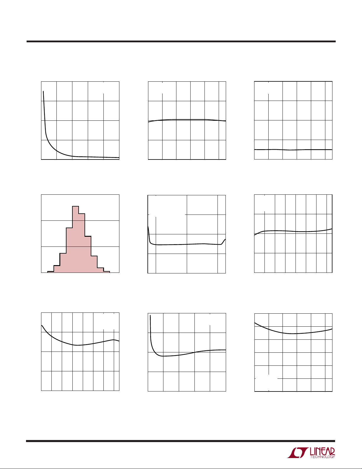
Conversion Current vs Temperature
230
220
210
200
190
180
SUPPLY CURRENT (µA)
170
160
150
–55
PSRR vs Frequency at V
–10
VCC = 4.1V
V
IN
–30
= 25°C
T
A
= 0
F
0
–50
–70
VCC = 5.5V
VCC = 4.1V
VCC= 2.7V
–30 –5 45
= 0V
20
TEMPERATURE (°C)
70 95 120
CC
2400 G19
Sleep Current vs Temperature
30
25
–30 –5
VCC = 2.7V, 5.5V
45 95 120
20 70
TEMPERATURE (°C)
20
15
10
SUPPLY CURRENT (µA)
5
0
–55
PSRR vs Frequency at V
0
VCC = 4.1V
= 0V
V
IN
–20
= 25°C
T
A
= 0
F
O
–40
–60
CC
2400 G20
PSRR vs Frequency at V
0
VCC = 4.1V
= 0V
V
IN
–20
= 25°C
T
A
= 0
F
O
–40
–60
REJECTION (dB)
–80
–100
–120
1
15,360Hz 153,600Hz
100 10k 1M
FREQUENCY AT VCC (Hz)
Rejection vs Frequency at V
CC
2400 G23
IN
REJECTION (dB)
–90
–110
–130
0
50 100 150 200
FREQUENCY AT VCC (Hz)
Rejection vs Frequency at V
–60
–70
–80
–90
–100
–110
REJECTION (dB)
–120
–130
–140
–12–8–404812
INPUT FREQUENCY DEVIATION FROM NOTCH FREQUENCY (%)
250
2400 G21
IN
2400 G25
REJECTION (dB)
–80
–100
–120
15200
15300 15350 15400
15250
FREQUENCY AT VCC (Hz)
Rejection vs Frequency at V
0
VCC = 5V
= 5V
V
REF
–20
= 2.5V
V
IN
= 0
F
O
–40
–60
REJECTION (dB)
–80
–100
–120
SAMPLE RATE = 15.36kHz ±2%
15100
15200 15300 15400 15500
FREQUENCY AT VIN (Hz)
15450 15500
1635 G22
IN
2400 G26
Rejection vs Frequency at V
IN
7
LTC2400
UW
TYPICAL PERFOR A CE CHARACTERISTICS
INL vs Output Rate Resolution vs Output Rate
24
22
20
18
16
INL (BITS)
14
12
10
8
0
VCC = 5V
= 5V
V
REF
= 25°C
T
A
F
= EXTERNAL
0
15 20 25105 303540455055
OUTPUT RATE (Hz)
2400 G27
60
24
22
20
18
16
14
RESOLUTION (BITS)*
12
10
8
UUU
PIN FUNCTIONS
*RESOLUTION =
0
15 20 25105 303540455055
VCC = 5V
V
T
F
/RMS NOISE)
LOG(V
REF
LOG (2)
OUTPUT RATE (Hz)
= 5V
REF
= 25°C
A
= EXTERNAL
O
2400 G28
60
VCC (Pin 1): Positive Supply Voltage. Bypass to GND
(Pin␣ 4) with a 10µF tantalum capacitor in parallel with
0.1µF ceramic capacitor as close to the part as possible.
V
(Pin 2): Reference Input. The reference voltage range
REF
is 0.1V to VCC.
VIN (Pin 3): Analog Input. The input voltage range is
–0.125 • V
to 1.125 • V
REF
REF
. For V
> 2.5V, the input
REF
voltage range may be limited by the pin absolute maximum rating of –0.3V to VCC + 0.3V.
GND (Pin 4): Ground. Shared pin for analog ground,
digital ground, reference ground and signal ground. Should
be connected directly to a ground plane through a minimum length trace or it should be the single-point-ground
in a single point grounding system.
CS (Pin 5): Active LOW Digital Input. A LOW on this pin
enables the SDO digital output and wakes up the ADC.
Following each conversion the ADC automatically enters
the Sleep mode and remains in this low power state as
long as CS is HIGH. A LOW on CS wakes up the ADC. A
LOW-to-HIGH transition on this pin disables the SDO
digital output. A LOW-to-HIGH transition on CS during the
Data Output transfer aborts the data transfer and starts a
new conversion.
SDO (Pin 6): Three-State Digital Output. During the data
output period, this pin is used for serial data output. When
the chip select CS is HIGH (CS = VCC), the SDO pin is in a
high impedance state. During the Conversion and Sleep
periods this pin can be used as a conversion status output.
The conversion status can be observed by pulling CS LOW.
SCK (Pin 7): Bidirectional Digital Clock Pin. In Internal
Serial Clock Operation mode, SCK is used as digital output
for the internal serial interface clock during the data output
period. In External Serial Clock Operation mode, SCK is
used as digital input for the external serial interface. A
weak internal pull-up is automatically activated in Internal
Serial Clock Operation mode. The Serial Clock mode is
determined by the level applied to SCK at power up and the
falling edge of CS.
FO (Pin 8): Frequency Control Pin. Digital input that
controls the ADC’s notch frequencies and conversion
time. When the FO pin is connected to VCC (FO = VCC), the
converter uses its internal oscillator and the digital filter
first null is located at 50Hz. When the FO pin is connected
to GND (FO = OV), the converter uses its internal oscillator
and the digital filter first null is located at 60Hz. When F
is driven by an external clock signal with a frequency f
O
EOSC,
the converter uses this signal as its clock and the digital
filter first null is located at a frequency f
EOSC
/2560.
8

LTC2400
3.4k
SDO
2400 TA04
HI-Z TO V
OL
VOH TO V
OL
VOL TO HI-Z
C
LOAD
= 20pF
V
CC
CONVERT
SLEEP
DATA OUTPUT
2400 F01
0
1
CS AND
SCK
UU
W
FU CTIO AL BLOCK DIAGRA
V
CC
GND
V
IN
V
REF
DAC
∫∫∫
∑
ADC
AUTOCALIBRATION
AND CONTROL
DECIMATING FIR
INTERNAL
OSCILLATOR
SERIAL
INTERFACE
(INT/EXT)
F
O
SDO
SCK
CS
2400 FD
TEST CIRCUITS
SDO
3.4k
HI-Z TO V
VOL TO V
OH
VOH TO HI-Z
U
OH
= 20pF
C
LOAD
2400 TA03
WUU
APPLICATIONS INFORMATION
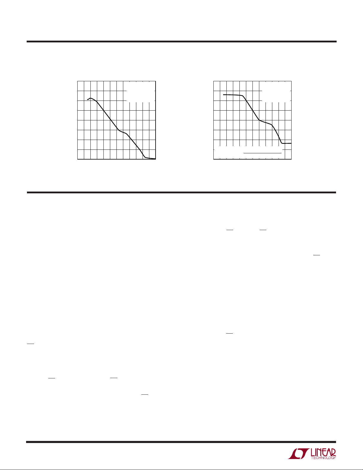
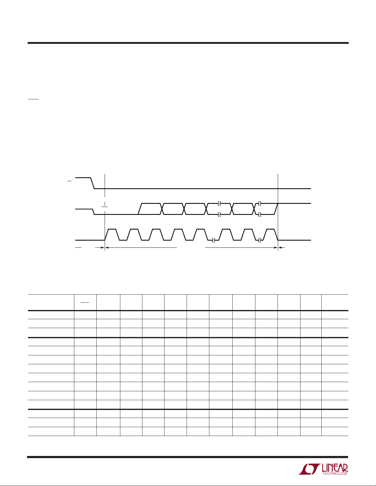
Converter Operation Cycle
The LTC2400 is a low power, delta-sigma analog-todigital converter with an easy to use 3-wire serial interface.
Its operation is simple and made up of three states. The
converter operating cycle begins with the conversion,
followed by a low power sleep state and concluded with
the data output (see Figure 1). The 3-wire interface consists of serial data output (SDO), a serial clock (SCK) and
a chip select (CS).
Initially, the LTC2400 performs a conversion. Once the
conversion is complete, the device enters the sleep state.
While in this sleep state, power consumption is reduced by
Figure 1. LTC2400 State Transition Diagram
9

LTC2400
U
WUU
APPLICATIONS INFORMATION
an order of magnitude. The part remains in the sleep state
as long as CS is logic HIGH. The conversion result is held
indefinitely in a static shift register while the converter is
in the sleep state.
Once CS is pulled low, the device begins outputting the
conversion result. There is no latency in the conversion
result. The data output corresponds to the conversion just
performed. This result is shifted out on the serial data out
pin (SDO) under the control of the serial clock (SCK). Data
is updated on the falling edge of SCK allowing the user to
reliably latch data on the rising edge of SCK, see Figure 3.
The data output state is concluded once 32 bits are read
out of the ADC or when CS is brought HIGH. The device
automatically initiates a new conversion cycle and the
cycle repeats.
Through timing control of the CS and SCK pins, the
LTC2400 offers several flexible modes of operation
(internal or external SCK and free-running conversion
modes). These various modes do not require programming configuration registers; moreover, they do not disturb the cyclic operation described above. These modes of
operation are described in detail in the Serial Interface
Timing Modes section.
Conversion Clock
A major advantage delta-sigma converters offer over
conventional type converters is an on-chip digital filter
(commonly known as Sinc or Comb filter). For high
resolution, low frequency applications, this filter is typically designed to reject line frequencies of 50 or 60Hz plus
their harmonics. In order to reject these frequencies in
excess of 110dB, a highly accurate conversion clock is
required. The LTC2400 incorporates an on-chip highly
accurate oscillator. This eliminates the need for external
frequency setting components such as crystals or oscillators. Clocked by the on-chip oscillator, the LTC2400
rejects line frequencies (50 or 60Hz ±2%) a minimum of
110dB.
conversion and the output data. Therefore, multiplexing
an analog input voltage is easy.
The LTC2400 performs offset and full-scale calibrations
every conversion cycle. This calibration is transparent to
the user and has no effect on the cyclic operation described above. The advantage of continuous calibration is
extreme stability of offset and full-scale readings with respect to time, supply voltage change and temperature drift.
Power-Up Sequence
The LTC2400 automatically enters an internal reset state
when the power supply voltage VCC drops below approximately 2.2V. This feature guarantees the integrity of the
conversion result and of the serial interface mode selection which is performed at the initial power-up. (See the
2-wire I/O sections in the Serial Interface Timing Modes
section.)
When the VCC voltage rises above this critical threshold,
the converter creates an internal power-on-reset (POR)
signal with duration of approximately 0.5ms. The POR
signal clears all internal registers. Following the POR
signal, the LTC2400 starts a normal conversion cycle and
follows the normal succession of states described above.
The first conversion result following POR is accurate
within the specifications of the device.
Reference Voltage Range
The LTC2400 can accept a reference voltage from 0V to
VCC. The converter output noise is determined by the
thermal noise of the front-end circuits, and as such, its
value in microvolts is nearly constant with reference
voltage. A decrease in reference voltage will not significantly improve the converter’s effective resolution. On the
other hand, a reduced reference voltage will improve the
overall converter INL performance. The recommended
range for the LTC2400 voltage reference is 100mV to VCC.
Input Voltage Range
Ease of Use
The LTC2400 data output has no latency, filter settling or
redundant data associated with the conversion cycle.
There is a one-to-one correspondence between the
10
The converter is able to accommodate system level offset
and gain errors as well as system level overrange situations due to its extended input range, see Figure 2. The
LTC2400 converts input signals within the extended input
range of –0.125 • V
to 1.125 • V
REF
REF
.
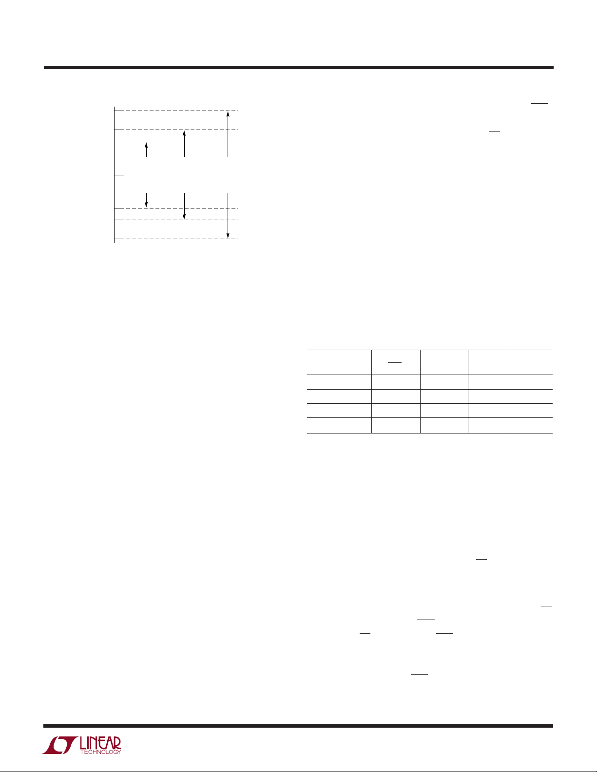
LTC2400
U
WUU
APPLICATIONS INFORMATION
VCC + 0.3V
9/8V
REF
V
REF
NORMAL
1/2V
–1/8V
REF
0
REF
–0.3V
INPUT
RANGE
Figure 2. LTC2400 Input Range
For large values of V
EXTENDED
INPUT
RANGE
this range is limited by the
REF
absolute maximum voltage range of – 0.3V to (VCC + 0.3V).
Beyond this range the input ESD protection devices begin
to turn on and the errors due to the input leakage current
increase rapidly.
Input signals applied to VIN may extend below ground by
–300mV and above VCC by 300mV. In order to limit any
fault current, a resistor of up to 5k may be added in series
with the VIN pin without affecting the performance of the
device. In the physical layout, it is important to maintain
the parasitic capacitance of the connection between this
series resistance and the VIN pin as low as possible;
therefore, the resistor should be located as close as
practical to the VIN pin. The effect of the series resistance
on the converter accuracy can be evaluated from the
curves presented in the Analog Input/Reference Current
section. In addition a series resistor will introduce a
temperature dependent offset error due to the input leakage current. A 1nA input leakage current will develop a
1ppm offset error on a 5k resistor if V
has a very strong temperature dependency.
Output Data Format
The LTC2400 serial output data stream is 32 bits long. The
first 4 bits represent status information indicating the
sign, input range and conversion state. The next 24 bits are
the conversion result, MSB first. The remaining 4 bits are
sub LSBs beyond the 24-bit level that may be included in
averaging or discarded without loss of resolution.
ABSOLUTE
MAXIMUM
INPUT
RANGE
2400 F02
= 5V. This error
REF
Bit 31 (first output bit) is the end of conversion (EOC)
indicator. This bit is available at the SDO pin during the
conversion and sleep states whenever the CS pin is LOW.
This bit is HIGH during the conversion and goes LOW
when the conversion is complete.
Bit 30 (second output bit) is a dummy bit (DMY) and is
always LOW.
Bit 29 (third output bit) is the conversion result sign indicator (SIG). If VIN is >0, this bit is HIGH. If VIN is <0, this
bit is LOW. The sign bit changes state during the zero code.
Bit 28 (forth output bit) is the extended input range (EXR)
indicator. If the input is within the normal input range
0␣ ≤␣VIN ≤ V
normal input range, VIN > V
, this bit is LOW. If the input is outside the
REF
or VIN < 0, this bit is HIGH.
REF
The function of these bits is summarized in Table 1.
Table 1. LTC2400 Status Bits
Bit 31 Bit 30 Bit 29 Bit 28
Input Range EOC DMY SIG EXR
VIN > V
REF
0 < VIN ≤ V
VIN = 0+/0
VIN < 0 0 001
REF
–
0 011
0 010
0 0 1/0 0
Bit 27 (fifth output bit) is the most significant bit (MSB).
Bits 27-4 are the 24-bit conversion result MSB first.
Bit 4 is the least significant bit (LSB).
Bits 3-0 are sub LSBs below the 24-bit level. Bits 3-0 may
be included in averaging or discarded without loss of
resolution.
Data is shifted out of the SDO pin under control of the serial
clock (SCK), see Figure 3. Whenever CS is HIGH, SDO
remains high impedance and any SCK clock pulses are
ignored by the internal data out shift register.
In order to shift the conversion result out of the device, CS
must first be driven LOW. EOC is seen at the SDO pin of the
device once CS is pulled LOW. EOC changes real time from
HIGH to LOW at the completion of a conversion. This
signal may be used as an interrupt for an external
microcontroller. Bit 31 (EOC) can be captured on the first
rising edge of SCK. Bit 30 is shifted out of the device on the
first falling edge of SCK. The final data bit (Bit 0) is shifted
11
LTC2400
U
WUU
APPLICATIONS INFORMATION
out on the falling edge of the 31st SCK and may be latched
on the rising edge of the 32nd SCK pulse. On the falling
edge of the 32nd SCK pulse, SDO goes HIGH indicating a
new conversion cycle has been initiated. This bit serves as
EOC (Bit 31) for the next conversion cycle. Table 2 summarizes the output data format.
As long as the voltage on the VIN pin is maintained within
the –0.3V to (VCC + 0.3V) absolute maximum operating
range, a conversion result is generated for any input value
from –0.125 • V
greater than 1.125 • V
SDO
to 1.125 • V
REF
REF
CS
Hi-Z
For input voltages
REF.
, the conversion result is clamped
BIT 31
EOC
BIT 28BIT 29BIT 30
to the value corresponding to 1.125 • V
voltages below –0.125 • V
, the conversion result is
REF
clamped to the value corresponding to –0.125 • V
. For input
REF
REF
.
Frequency Rejection Selection (FO Pin Connection)
The LTC2400 internal oscillator provides better than 110dB
normal mode rejection at the line frequency and all its
harmonics for 50Hz ±2% or 60Hz ±2%. For 60Hz rejection, FO (Pin 8) should be connected to GND (Pin 4) while
for 50Hz rejection the FO pin should be connected to V
CC
(Pin␣ 1).
BIT 0BIT 27 BIT 4
MSBEXTSIG“0”
LSB
24
SCK
SLEEP DATA OUTPUT CONVERSION
1 2 3 4 5 272832
2400 F03
Figure 3. Output Data Timing
Table 2. LTC2400 Output Data Format
Bit 31 Bit 30 Bit 29 Bit 28 Bit 27 Bit 26 Bit 25 Bit 24 Bit 23 … Bit 4 Bit 3-0
Input Voltage EOC DMY SIG EXR MSB LSB SUB LSBs*
VIN > 9/8 • V
9/8 • V
V
REF
V
REF
3/4V
3/4V
1/2V
1/2V
1/4V
1/4V
0+/0
–1LSB 0 0 0111 1 11...1 X
–1/8 • V
VIN < –1/8 • V
*The sub LSBs are valid conversion results beyond the 24-bit level that may be included in averaging or discarded without loss of resolution.
**The sign bit changes state during the 0 code.
REF
REF
+ 1LSB 0 0 1 1 0 0 0 0 0 ... 0 X
+ 1LSB 0 0 1 0 1 1 0 0 0 ... 0 X
REF
REF
+ 1LSB 0 0 1 0 1 0 0 0 0 ... 0 X
REF
REF
+ 1LSB 0 0 1 0 0 1 0 0 0 ... 0 X
REF
REF
–
REF
REF
001100011...1X
001100011...1X
001011111...1X
001010111...1X
001001111...1X
001000111...1X
0 0 1/0** 0 0 0 0 0 0 ... 0 X
000111100...0X
000111100...0X
12
 Loading...