

Datasheet LTC2383-16, TC2383-16, LTC2382-16, TC2382-16, LTC2381-16 Datasheet (LINEAR TECHNOLOGY)
...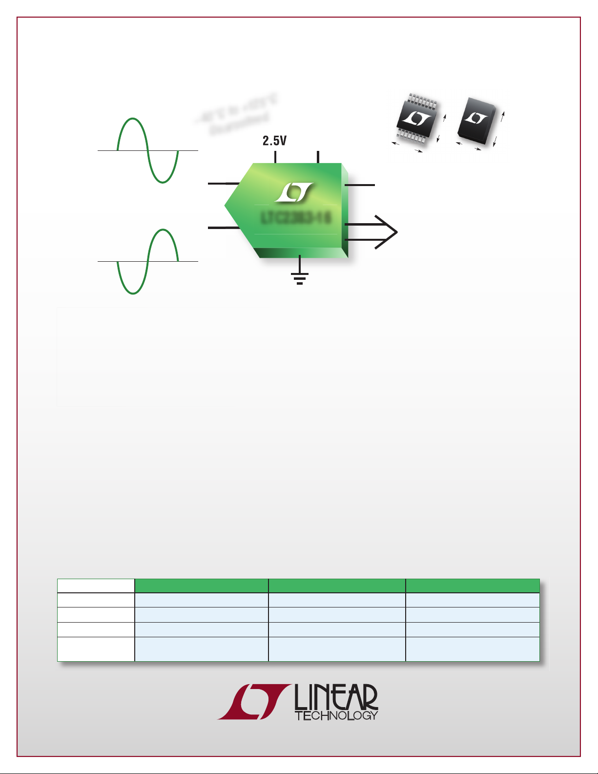
LTC2383: 16-Bit, 1Msps, 13mW SAR ADC
LTC2383-16
LTC2382-16
LTC2381-16
– 40°C to +125°C
Guaranteed
+
2.5V2.5V
5mm
MSOP-16
IN+
OV
= 1.8V to 5V
DD
Fully Differential
±2.5V Input
IN–
LTC2383-16
3-Wire
SPI Interface
–
The LTC®2383-16 is a 1Msps, no latency SAR ADC that offers low 13mW power consumption, 92dB SNR using a fully differential
input range, ±2LSB INL (max) and 16-bit no missing codes resolution. The pin- and software-compatible family includes
LTC2382-16 (500ksps) and LTC2381-16 (250ksps) and features a proprietary sampling architecture that allows the use of
extremely low power ADC drivers, thus reducing the overall power consumption of the entire data acquisition solution. To achieve
uncompromised AC performance, we recommend the fast settling LT
of input signals. We also recommend the LTC6652-2.5, a precision external reference with high accuracy, low power and small
size. The –40°C to 125°C temperature range of LT6350 and LTC6652 complements that of LTC2383 family and makes them ideal
for automotive applications.
®
6350 ADC driver for single-ended to differential conversion
4mm
4mm
3mm
DFN-16
Features
n
±2LSB INL (Max), ±1LSB DNL (Max)
n
Low Power: 13mW at 1Msps, 13µW at 1ksps
n
92dB SNR (Typ) at fIN = 20kHz
n
Guaranteed Operation to 125°C
n
2.5V Supply
n
Fully Differential Input Range ±2.5V
n
External 2.5V Reference Input
n
No Pipeline Delay, No Cycle Latency
n
1.8V to 5V I/O Voltages
n
SPI-Compatible Serial I/O with Daisychain Mode
n
Internal Conversion Clock
LTC2383-16
Resolution
Speed
Power
Package
16-Bit 16-Bit 16-Bit
1Msps 500ksps 250ksps
13mW 6.5mW 3.25mW
4mm × 3mm DFN-16,
16-Lead MSOP
Applications
n
Medical Imaging
n
High Speed Data Acquisition
n
Portable or Compact Instrumentation
n
Industrial Process Control
n
Low Power Battery-Operated Instrumentation
n
ATE
LTC2382-16
4mm × 3mm DFN-16,
16-Lead MSOP
LTC2381-16
4mm × 3mm DFN-16,
16-Lead MSOP
L, LT, LTC, LTM, Linear Technology and the Linear logo are registered
trademarks of Linear Technology Corporation. All other trademarks are the
property of their respective owners.
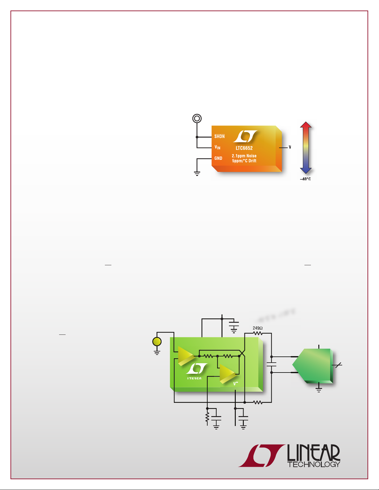
LTC6652: Precision, Low Drift, Low Noise ADC Reference
www.linear.com/2383
The LTC6652 is a precision, low noise, series voltage reference offered in seven output voltage options: 1.25V, 2.048V, 2.5V, 3.0V,
3.3V, 4.096V and 5V. Along with an initial accuracy of 0.05%, and maximum voltage drift of 5ppm/°C, the LTC6652 offers excellent
load and line regulation, and noise of only 2.1ppm. The combination of precision and low noise makes the LTC6652 ideal for
precision data acquisition and medical instrumentation. With an output current drive of ±5mA, the LTC6652 provides a highly
accurate ADC voltage reference without the need of a separate buffer. No load capacitor is required, helping to minimize board
space. The LTC6652 is fully specified over –40°C to 125°C, making it suitable for high performance, high temperature industrial
and automotive applications.
Features
n
Voltage Options: 1.25V, 2.048V, 2.5V, 3V, 3.3V, 4.096V, 5V
n
Fully Specified Over –40°C to 125°C
n
0.05% Initial Accuracy and 5ppm/°C Drift (A-Grade)
n
Low Noise: 2.1ppm/V
n
±5mA Sink and Source Capability
n
Low Power Shutdown: <2µA Maximum
n
300mV Dropout Voltage
n
Line Regulation: 50ppm/V Maximum
n
Load Regulation: 75ppm/mA Maximum
n
No External Load Capacitor Required
n
Wide Supply Range to 13.2V
n
8-Lead MSOP Package
(0.1Hz to 10Hz)
P-P
+
V
125°C
V
REF
No Caps Required
–40°C
LT6350: Low Noise, Single-Ended to Differential ADC Driver
The LT6350 is a 33MHz, low noise, rail-to-rail input and output ADC driver that settles to 16 bits in just 350ns. It is suitable for
driving the latest high performance SAR ADCs, such as the LTC2383-16. The LT6350 incorporates two op amps and matched
resistors to create a differential output from a single-ended high impedance input. As a result, a differential gain of 2 is achieved
with no external feedback resistors and higher gain can be obtained by using feedback resistors. Each of the two internal op
amps achieves a low 1.9nV/√Hz input-referred noise density, resulting in a total output referred noise of just 8.2nV/√Hz. The
LT6350 enables high performance ADCs to achieve better than 110dB SNR over a 1MHz bandwidth. Operating from a 2.7V to
12V total supply, the LT6350 consumes 4.8mA supply current and has a shutdown mode that allows the system to reduce power
consumption during periods of inactivity.
Features
n
Rail-to-Rail Input and Outputs
n
Fast Settling Time: 240ns, 0.01%,
Output Step
8V
P-P
n
1.9nV/√Hz Input-Referred
Op Amp Noise
n
High Impedance Input
n
–3dB Bandwidth: 33MHz
n
2.7V to 12V Supply Operation
n
No External Gain Resistors Required
n
Low Offset Voltage: ±400µV Max
n
High DC Linearity: <±1LSB, 16-Bit, 8V
n
Low Distortion (HD2/HD3): –102dBc/–97dBc
at 100kHz, V
n
Low Power Shutdown
n
3mm × 3mm 8-Pin DFN and
OUTDIFF
= 4V
P-P
8-Lead MSOP Packages
www.linear.com/2383 n 1-800-4-LINEAR
0V TO 4V
P-P
5V
– 40°C to +125°C
0.1μF
249Ω
V
IN
+
–
+
IN1
SHDN
+
–
LT6350
–
IN1
499Ω
+
IN2
2V
+
V
OUT2
–
+
–
OUT1
V
0.1μF 0.1μF
–5V
249Ω
2200pF
–
A
IN
LTC2383-16
+
A
IN
2.5V
0810A
 Loading...