

Upgrade Your Microcontroller ADC to True 12-Bit Performance
Design Note DN463
by Guy Hoover
Introduction
Many 8-bit and 16-bit microcontrollers feature 10-bit
internal ADCs. A few include 12-bit ADCs, but these often
have poor or nonexistent AC specifi cations, and certainly
lack the performance to meet the needs of an increasing
®
number of applications. The LTC
2366 and its slower
speed versions offer a high performance alternative, as
shown in the AC specifi cations in Table 1. Compare these
guaranteed specifi cations with the ADC built into your
current microcontroller.
This family’s DC specifi cations ar e equally impressive. INL
and DNL are guaranteed to be less than ±1LSB. Operating
from a single 2.5V, 3V or 3.3V supply, the current draw
on these parts is a maximum of 4mA during a conversion. This can be reduced to less than 1μA by placing
the part into SLEEP mode during periods of inactivity,
These ADCs are available in tiny 6-lead and 8-lead TSOT23 packages. The 8-lead devices have adjustable V
and OV
span to be reduced to 1.4V. This, combined with the high
ADC input impedance, can eliminate the need for gain or
buf fer s tages in many applications. The OV
controls the digital output level, can be adjusted from 1V
to 3.6V, simplifying communication with different logic
families. For applications that do not require an adjust able
reference or adjustable output levels, the 6-lead device
with V
The SPI inter face requires only t hree wires to communicate
with the microcontroller, keeping the overall solution size
small in low power, high speed applications.
L, LT, LTC and LTM are registered trademarks of Linear Technology Corporation.
All other trademarks are the property of their respective owners.
which greatl y reduces the average supply current a t lower
sample rates.
C3
0.1μF
R2
1k
AGND
A
IN
R4
499Ω
C2
1μF
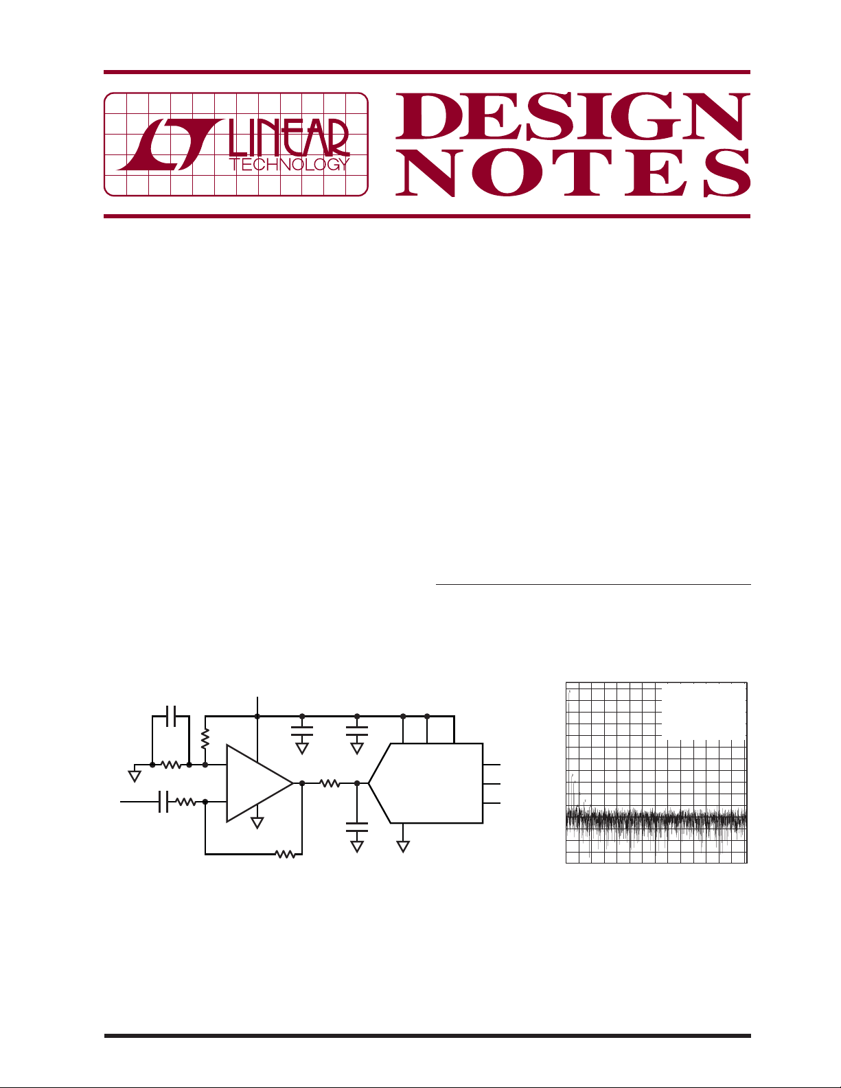
Figure 1. Single Supply AC-Coupled Amplifi er Level Shifts Input for
Maximum Dynamic Range
R1
1k
AV=–4
+
LT6202
–
3.3V
AGND
0.1μF
2.0k
C5
AGND
R5
24.9Ω
0.0047μF
R3
C4
10μF
12 5
V
AGND
C1
AGND
DDVREFOVDD
A
IN
GND
AGND
LTC2366
3
pins. The adjustable V
DD
= OVDD = VDD should suffi ce.
REF
0
–20
–40
CS
SCK
SDO
dn463 F01
8
7
6
–60
–80
–100
FOURIER TRANSFORM
–120
–140
0
Figure 2. FFT Shows Low Noise and
Distortion of Figure 1 Circuit
pin allows the input
REF
pin, which
DD
8192 Pt FFT
= 2.84MHz
f
S
= –1dB AT 20kHz
V
IN
SNR = 72.1dB
THD = –70.1dB
0.4 0.80.2 0.6 1.21.0
FREQUENCY (MHz)
REF
dn463 F02
1.4
04/09/463
Application Circuits
Figure 1 shows a single supply AC-coupled amplifi er
driving the LTC2366. This circuit is useful in applications where the sensor output level is too low to achieve
full SNR performance from the ADC. The output of the
®
6202 swings rail-to-rail. This feature maximizes the
LT
circuit’s dynamic range when the op amp output is level
shifted to the center of the ADC’s swing. The FFT of
Figure 2 demonstrates the low noise and distortion of
this circuit.
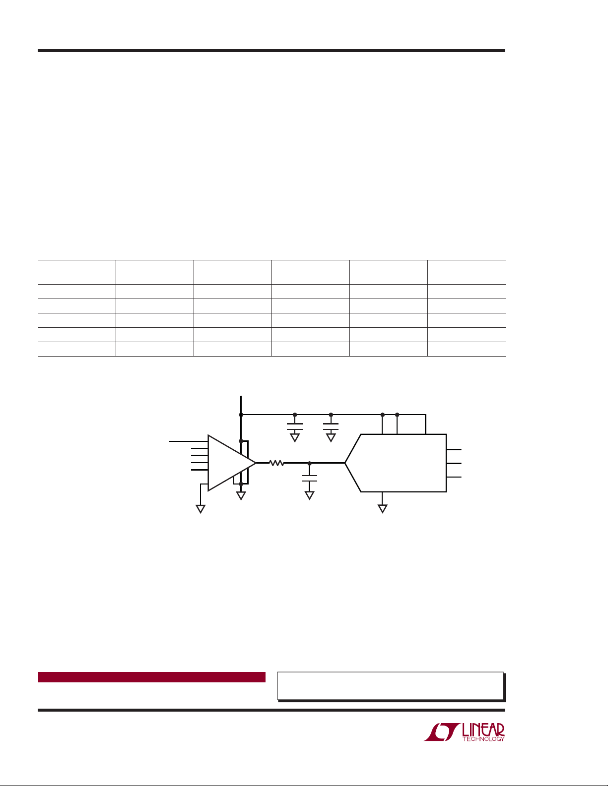
In Figure 3, a single supply DC amplifi er with a program-
the LTC6915 is a good choice for high gain applications.
This circuit is useful for very low level signals or for applications with a wide range of input levels.
Conclusion
The 12-bit ADCs in the LTC236x family guarantee AC
specifi cations that most built-in microcontroller ADCs
cannot meet, thus improving performance when used
in place of on-chip ADCs. The LTC236x family is easily
interfaced to most microcontrollers via its SPI interface.
A wide range of sample rates, an external reference pin
and a separate OV
pin provide additional fl exibility.
DD
mable gain of 0 to 4096 drives the LTC2360. With a maximum of fse t of 10μV and a DC to 10Hz noise of 2.5μV
Table 1. LTC236x ADC Family AC Specifi cations
PART NUMBER SAMPLE RATE SINAD SNR THD
LTC2366 3Msps 68dB (Min) 69dB (Min) –72dB (Max) 2.5MHz (Typ)
LTC2365 1Msps 68dB (Min) 70dB (Min) –72dB (Max) 2.0MHz (Typ)
LTC2362 500ksps 72dB (Typ) 73dB (Typ) –85dB (Typ) 1.0MHz (Typ)
LTC2361 250ksps 72dB (Typ) 73dB (Typ) –85dB (Typ) 1.0MHz (Typ)
LTC2360 100ksps 72dB (Typ) 73dB (Typ) –85dB (Typ) 1.0MHz (Typ)
P–P
,
FULL LINEAR
BANDWIDTH
D3 D2 D1 D0 GAIN
0 0 0 0 0
0 0 0 1 1
0 0 1 0 2
0 0 1 1 4
0 1 0 0 8
0 1 0 1 16
0 1 1 0 32
0 1 1 1 64
1 0 0 0 128
1 0 0 1 256
1 0 1 0 512
1 0 1 1 1024
1 1 0 0 2048
1 1 0 1 4096
1 1 1 0 4096
1 1 1 1 4096
Data Sheet Download
www.linear.com
3.3V
C10
A
IN
D0
D1
D2
D3
+
LTC6915
–
AGND
REF
+
V
–
V
AGND
P/SL
DGND
R10
24.9Ω
0.1μF
AGND
AGND
AGND
C6
300pF
4
C9
10μF
12 5
V
DDVREF
A
IN
GND
3
AGND
LTC2360
OV
DD
CSL
SCK
SDO
dn463 F03
Figure 3. Single Supply DC Amplifi er Provides Programmable Gain from 0 to 4096
For applications help,
call (408) 432-1900, Ext. 2602
8
7
6
Linear Technology Corporation
1630 McCarthy Blvd., Milpitas, CA 95035-7417
(408) 432-1900
●
FAX: (408) 434-0507 ● www.linear.com
dn463 LT/TP 0409 155K • PRINTED IN THE USA
© LINEAR TECHNOLOGY CORPORATION 2009
 Loading...