

Page 1
QUICK START GUIDE FOR DEMONSTRATION CIRCUIT 1190
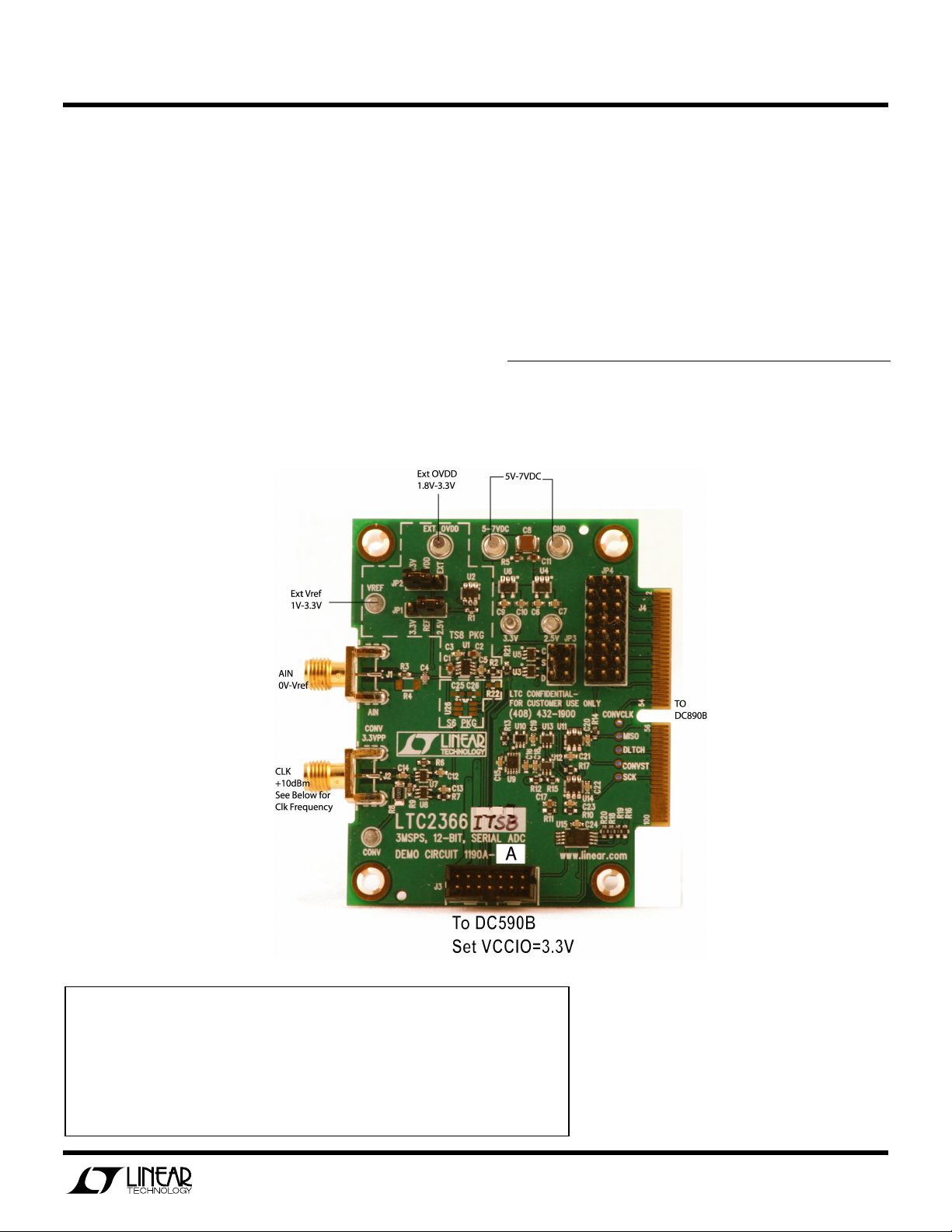
Figure
1. DC1190A
Connection Diagram
DESCRIPTION
3MSPS, 12-BIT, SERIAL ADC
LTC2360/61/62/65/66
Demonstration circuit 1190 features the LTC2360
family. With up to 3MSPS these unipolar, single
channel, 12-Bit, SPI compatible serial ADCs are
available in 6- or 8-Lead TSOT packages. The 8Lead package has external V
the 6-pin version has Vref and OVDD internally
connected to the VDD supply pin. The following text
refers to the LTC2366 but applies to all members
of the family. DC1190 demonstrates the DC and AC
performance of the LTC2366 in conjunction with
and OVDD pins while
REF
the DC590B Quick Eval and DC890B Fast DAACS
data collection boards. Alternatively, by connecting
the DC1190 into a customer application the
performance of the LTC2366 can be evaluated
directly in that circuit.
Design files for this circuit board are available.
Call the LTC factory.
LTC is a trademark of Linear Technology Corporation
Demo Board IC Max Clk Frequency
DC1190A-A LTC2366ITS8 48MHz
DC1190A-B LTC2365ITS8 16MHz
DC1190A-C LTC2362ITS8 50MHz
DC1190A-D LTC2361ITS8 25MHz
DC1190A-E LTC2360ITS8 10MHz
1
Page 2

QUICK START GUIDE FOR DEMONSTRATION CIRCUIT 1190
DC890B QUICK START PROCEDURE
3MSPS, 12-BIT, SERIAL ADC
Connect DC1190 to a DC890B USB High Speed Data
Collection Board using connector J4. Connect
DC890B to a host PC with a standard USB A/B
cable. Apply 5V-7V DC to the 5-7VDC and GND
terminals. Apply a low jitter signal source to J1. As
a clock source, apply a low jitter 10dBm sine wave
or square wave to connector J2. See table on page
1 for maximum frequencies. Note that J2 has a 50ohm termination resistor to ground. Run the
QuickEval-II software (Pscope.exe version K51 or
later) supplied with DC890B or download it from
DC590B QUICK START PROCEDURE
Connect DC1190 to a DC590B USB serial controller
using the supplied 14-conductor ribbon cable.
Make sure that VCCIO of DC590B is set to 3.3V
Connect DC590B to a host PC with a standard USB
A/B cable. Apply a signal source to J1. Run the
.
HARDWARE SET UP
www.linear.com. Complete software documentation
is available from the Help menu. Updates can be
downloaded from the Tools menu. Check for
updates periodically as new features may be added.
The Pscope software should recognize DC1190 and
configure itself automatically.
Click the Collect button (See Figure 2) to begin
acquiring data. The Collect button then changes to
Pause, which can be used to pause data acquisition.
evaluation software supplied with DC590B or
download it from www.linear.com. The correct
control panel will be loaded automatically. Click the
COLLECT (Figure 3) button to begin reading the
ADC.
SIGNAL CONNECTIONS
J1 SMA connector for AIN. Limit input voltage
swings to GND-V
the input should be bandlimited to the
frequencies of interest.
J2 Conversion Clock Input. This input has a 50-ohm
termination resistor, and is intended to be driven by
a low jitter, 10dBm sine or square wave. To achieve
full AC performance of this part, the clock jitter
should be kept under 20ps. This input is
capacitively coupled so that the input clock can be
either 0V-3.3V or ±1.65V so that level shifting is not
required. To run at the maximum conversion rate,
apply the frequency specified in the table on page 1.
J3 Quick Eval interface. Connect to DC590B.
sure that VCCIO of DC590B is set to 3.3V
. For optimum performance,
REF
.
Make
J4 FastDAACS interface. Connect to DC890B. Do
not connect to both DC590 and DC890 at the same
time.
VREF External V
used to monitor the internal Vref voltage. To use
this pin as an external V
JP1.
EXT OVDD External OVDD connection. This can be
used to drive the SDO output to logic levels other
than 3.3V. To use this pin put jumper JP2 in the
EXT position and apply desired OVDD voltage.
JP1 Reference voltage select. Use this jumper to
select the ADC reference voltage. Options include
2.5V, 3.3V or an external reference voltage can be
applied by removing the jumper and applying a
voltage to VREF.
JP2 OVDD select. Set OVDD to 3.3V or an external
voltage.
connection or it can also be
REF
input remove jumper
REF
2
Page 3

QUICK START GUIDE FOR DEMONSTRATION CIRCUIT 1190
3MSPS, 12-BIT, SERIAL ADC
JP3 I/O lines for ADC. See schematic for pinout.
JP4 Factory use only. There should be a jumper
from pins 8-16 for LTC2365 and LTC2366. There
should be a jumper from pins 16-24 for LTC2362,
LTC2361, and LTC2360.
GROUNDING AND POWER CONNECTION
Connect a 5V to 7V power supply to the 5-7VDC
and GND input connectors. For
Figure 2. DC1190 Fast DAACS Screenshot
Do not make connections to any other pins on this
connector.
optimum performance, this supply should be
floating with respect to any signal generators
connected to the analog input (J1)
3
Page 4

QUICK START GUIDE FOR DEMONSTRATION CIRCUIT 1190
3MSPS, 12-BIT, SERIAL ADC
Figure 3. DC1190 Quick Eval Screenshot
4
Page 5

QUICK START GUIDE FOR DEMONSTRATION CIRCUIT 1190
3MSPS, 12-BIT, SERIAL ADC
5
Page 6

QUICK START GUIDE FOR DEMONSTRATION CIRCUIT 1190
3MSPS, 12-BIT, SERIAL ADC
6
 Loading...