

FEATURES
FREQUENCY (MHz)
0.1
–80
THD, 2nd, 3rd (dB)
–74
–68
–62
–56
1 10 100
2356 G02
–86
–92
–98
–104
–50
THD
2nd
3rd
LTC2356-12/LTC2356-14
Serial 12-Bit/14-Bit, 3.5Msps
Sampling ADCs with Shutdown
U
DESCRIPTIO
■
3.5Msps Conversion Rate
■
74.1dB SINAD at 14-Bits, 71.1dB SINAD at 12-Bits
■
Low Power Dissipation: 18mW
■
3.3V Single Supply Operation
■
2.5V Internal Bandgap Reference can be Overdriven
■
3-Wire SPI-Compatible Serial Interface
■
Sleep (13µW) Shutdown Mode
■
Nap (4mW) Shutdown Mode
■
80dB Common Mode Rejection
■
±1.25V Bipolar Input Range
■
Tiny 10-Lead MSOP Package
U
APPLICATIO S
■
Communications
■
Data Acquisition Systems
■
Uninterrupted Power Supplies
■
Multiphase Motor Control
■
Multiplexed Data Acquisition
■
RFID
The LTC®2356-12/LTC2356-14 are 12-bit/14-bit, 3.5Msps
serial ADCs with differential inputs. The devices draw
only 5.5mA from a single 3.3V supply and come in a tiny
10-lead MSOP package. A Sleep shutdown feature further
reduces power consumption to 13µW. The combination of
speed, low power and tiny package makes the LTC2356-12/
LTC2356-14 suitable for high speed, portable applications.
The 80dB common mode rejection allows users to eliminate ground loops and common mode noise by measuring
signals differentially from the source.
The devices convert –1.25V to 1.25V bipolar inputs differentially. The absolute voltage swing for A
–
A
extends from ground to the supply voltage.
IN
IN
+
and
The serial interface sends out the conversion results during
the 16 clock cycles following a CONV rising edge for
compatibility with standard serial interfaces. If two additional clock cycles for acquisition time are allowed after the
data stream in between conversions, the full sampling rate
of 3.5Msps can be achieved with a 63MHz clock.
, LT, LTC and LTM are registered trademarks of Linear Technology Corporation.
All other trademarks are the property of their respective owners.
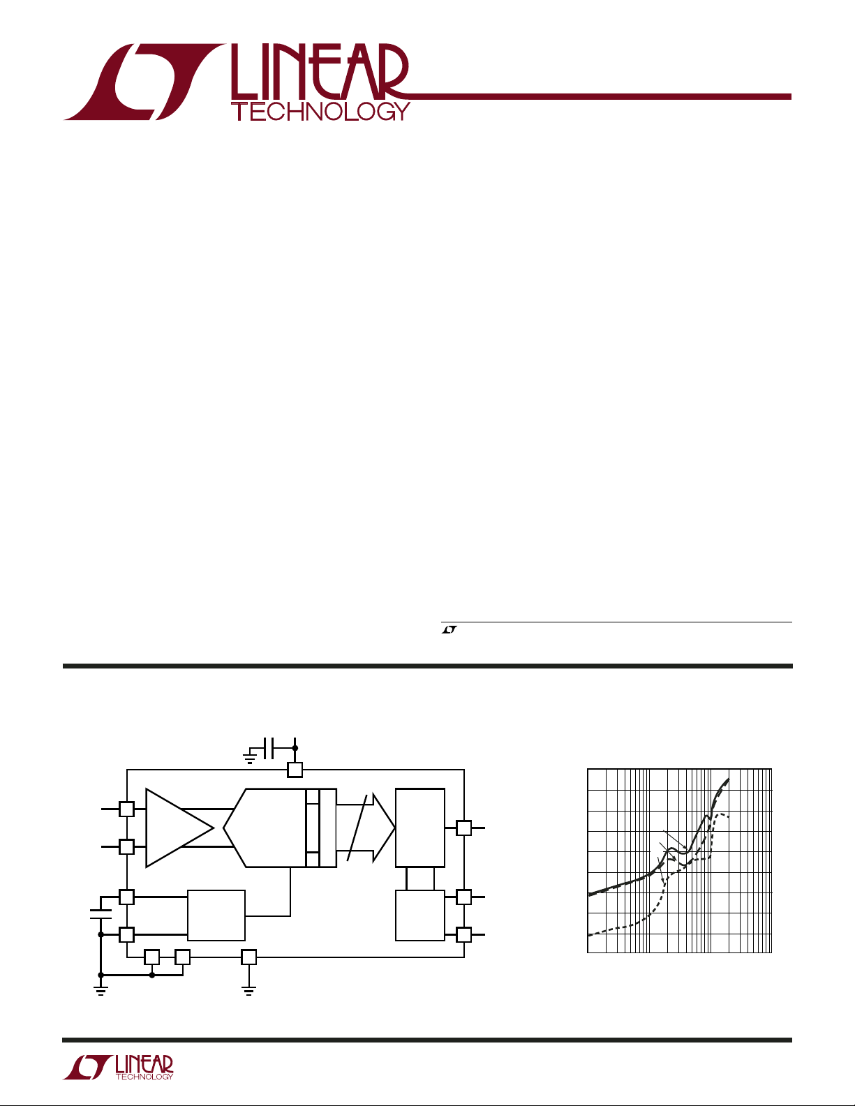
BLOCK DIAGRA
10µF
LTC2356-14
+
A
IN
–
A
IN
+
1
S & H
2
–
V
REF
3
GND
4
5 6 11
2.5V
REFERENCE
W
14-BIT ADC
EXPOSED PAD
3.3V10µF
THD, 2nd and 3rd vs Input Frequency
for Differential Input Signals
7
V
DD
THREE-
14-BIT LATCH
14
STATE
SERIAL
OUTPUT
PORT
TIMING
LOGIC
SDO
8
CONV
10
SCK
9
2356 BD
2356f
1
LTC2356-12/LTC2356-14
1
2
3
4
5
A
IN
+
A
IN
–
V
REF
GND
GND
10
9
8
7
6
CONV
SCK
SDO
V
DD
GND
TOP VIEW
11
MSE PACKAGE
10-LEAD PLASTIC MSOP
WWWU
ABSOLUTE AXI U RATI GS
(Notes 1, 2)
Supply Voltage (VDD) ................................................. 4V
Analog and V
(Note 3) ....................................– 0.3V to (V
Digital Input Voltages ................. – 0.3V to (V
Digital Output Voltage .................. – 0.3V to (V
Power Dissipation.............................................. 100mW
Operation Temperature Range
LTC2356C-12/LTC2356C-14 ................... 0°C to 70°C
LTC2356I-12/LTC2356I-14 ................ – 40°C to 85°C
Storage Temperature Range ................. –65°C to 150°C
Lead Temperature (Soldering, 10 sec).................. 300°C
Input Voltages
REF
+ 0.3V)
DD
+ 0.3V)
DD
+ 0.3V)
DD
UU
W
PACKAGE/ORDER I FOR ATIO
ORDER PART
NUMBER
LTC2356CMSE-12
LTC2356IMSE-12
LTC2356CMSE-14
LTC2356IMSE-14
MSE PART MARKING
T
= 125°C, θJA = 150°C/ W
JMAX
EXPOSED PAD (PIN 11) IS GND
MUST BE SOLDERED TO PCB
Order Options Tape and Reel: Add #TR
Lead Free: Add #PBF Lead Free Tape and Reel: Add #TRPBF
Lead Free Part Marking: http://www.linear.com/leadfree/
Consult factory for parts specified with wider operating temperature ranges.
LTCWN
LTCWN
LTCVF
LTCVF
CO VERTER CHARACTERISTICS
temperature range, otherwise specifications are at T
PARAMETER CONDITIONS MIN TYP MAX MIN TYP MAX UNITS
Resolution (No Missing Codes)
Integral Linearity Error (Notes 4, 5, 18)
Offset Error (Notes 4, 18)
Gain Error (Note 4, 18)
Gain Tempco Internal Reference (Note 4) ±15 ±15 ppm/°C
A ALOG I PUT
otherwise specifications are at T
SYMBOL PARAMETER CONDITIONS MIN TYP MAX UNITS
V
V
I
C
t
t
t
CMRR Analog Input Common Mode Rejection Ratio fIN = 1MHz, VIN = 0V to 3V –60 dB
2
U
UU
IN
CM
IN
IN
ACQ
AP
JITTER
Analog Differential Input Range (Notes 3, 8, 9) 3.1V ≤ VDD ≤ 3.6V
Analog Common Mode + Differential 0 to V
Input Range (Note 10)
Analog Input Leakage Current
Analog Input Capacitance (Note 19) 13 pF
Sample-and-Hold Acquisition Time (Note 6)
Sample-and-Hold Aperture Delay Time 1 ns
Sample-and-Hold Aperture Delay Time Jitter 0.3 ps
The ● denotes the specifications which apply over the full operating
= 25°C. With internal reference. VDD = 3.3V
A
LTC2356-12 LTC2356-14
●
12 14 Bits
●
–2 ±0.25 2 –4 ±0.5 4 LSB
●
–10 ±1 10 –30 ±230 LSB
●
–40 ±5 40 –80 ±10 80 LSB
External Reference ±1 ±1 ppm/°C
The ● denotes the specifications which apply over the full operating temperature range,
= 25°C. With internal reference. VDD = 3.3V
A
●
●
●
f
= 100MHz, VIN = 0V to 3V –15 dB
IN
–1.25 to 1.25 V
DD
1 µA
39 ns
V
2356f
LTC2356-12/LTC2356-14
U
W
DY A IC ACCURACY
otherwise specifications are at T
DC. Differential signal drive with V
SYMBOL PARAMETER CONDITIONS MIN TYP MAX MIN TYP MAX UNITS
SINAD Signal-to-Noise Plus 100kHz Input Signal (Note 19) 71.1 74.1 dB
Distortion Ratio 1.4MHz Input Signal (Note 19)
THD Total Harmonic 100kHz First 5 Harmonics (Note 19) –86 –86 dB
Distortion 1.4MHz First 5 Harmonics (Note 19)
SFDR Spurious Free 100kHz Input Signal (Note 19) 86 86 dB
Dynamic Range 1.4MHz Input Signal (Note 19) 82 82 dB
IMD Intermodulation 0.625V
Distortion 1.56MHz into A
Code-to-Code V
Transition Noise
Full Power Bandwidth VIN = 2.5V
Full Linear Bandwidth S/(N + D) ≥ 68dB 5 5 MHz
= 25°C with external reference = 2.55V. VDD = 3.3V. Single-ended A
A
REF
The ● denotes the specifications which apply over the full operating temperature range,
= 1.5V at A
CM
1.4MHz Summed with 0.625V
P-P
= 2.5V (Note 18) 0.25 1 LSB
P-P
+
and A
IN
+
and Inverted into A
IN
, SDO = 11585LSB
–
IN
LTC2356-12 LTC2356-14
●
68 71.1 70 72.3 dB
●
P-P
–
IN
(Note 15) 50 50 MHz
P-P
–82 –76 –82 –78 dB
–82 –82 dB
+
signal drive with A
IN
–
IN
= 1.5V
RMS
UU U
I TER AL REFERE CE CHARACTERISTICS
full operating temperature range, otherwise specifications are at T
= 25°C. VDD = 3.3V
A
The ● denotes the specifications which apply over the
PARAMETER CONDITIONS MIN TYP MAX UNITS
V
Output Voltage I
REF
V
Output Tempco 15 ppm/°C
REF
V
Line Regulation VDD = 3.1V to 3.6V, V
REF
V
Output Resistance Load Current = 0.5mA 0.2 Ω
REF
V
Settling Time C
REF
External V
Input Range 2.55 V
REF
= 0 2.5 V
OUT
= 2.5V 600 µV/V
REF
= 10µF2ms
REF
DD
UU
DIGITAL I PUTS A D DIGITAL OUTPUTS
full operating temperature range, otherwise specifications are at T
SYMBOL PARAMETER CONDITIONS MIN TYP MAX UNITS
V
IH
V
IL
I
IN
C
IN
V
OH
V
OL
I
OZ
C
OZ
I
SOURCE
I
SINK
High Level Input Voltage VDD = 3.6V
Low Level Input Voltage VDD = 3.1V
Digital Input Current VIN = 0V to V
Digital Input Capacitance 5pF
High Level Output Voltage VDD = 3.3V, I
Low Level Output Voltage VDD = 3.1V, I
= 3.1V, I
V
DD
Hi-Z Output Leakage D
Hi-Z Output Capacitance D
Output Short-Circuit Source Current V
Output Short-Circuit Sink Current V
OUT
OUT
V
OUT
OUT
OUT
= 25°C. VDD = 3.3V
A
DD
OUT
OUT
OUT
= 0V to V
= 0V, VDD = 3.3V 20 mA
= VDD = 3.3V 15 mA
DD
The ● denotes the specifications which apply over the
●
2.4 V
●
●
= – 200µA
= 160µA 0.05 V
= 1.6mA
●
2.5 2.9 V
●
●
0.10 0.4 V
1pF
0.6 V
± 10 µA
± 10 µA
V
2356f
3
LTC2356-12/LTC2356-14
WU
POWER REQUIRE E TS
range, otherwise specifications are at T
SYMBOL PARAMETER CONDITIONS MIN TYP MAX UNITS
V
DD
I
DD
P
D
Supply Voltage 3.1 3.3 3.6 V
Supply Current Active Mode
Power Dissipation Active Mode with SCK in Fixed State (Hi or Lo) 18 mW
= 25°C. (Note 17)
A
The ● denotes the specifications which apply over the full operating temperature
●
Nap Mode
●
Sleep Mode (LTC2356-12) 4 15 µA
Sleep Mode (LTC2356-14) 4 12 µA
5.5 8 mA
1.1 1.5 mA
WU
TI I G CHARACTERISTICS
range, otherwise specifications are at T
SYMBOL PARAMETER CONDITIONS MIN TYP MAX UNITS
f
SAMPLE(MAX)
t
THROUGHPUT
t
SCK
t
CONV
t
1
t
2
t
3
t
4
t
5
t
6
t
7
t
8
t
9
t
10
t
12
Note 1: Stresses beyond those listed under Absolute Maximum Ratings
may cause permanent damage to the device. Exposure to any Absolute
Maximum Rating condition for extended periods may affect device
reliability and lifetime.
Note 2: All voltage values are with respect to GND.
Note 3: When these pins are taken below GND or above V
clamped by internal diodes. This product can handle input currents greater
than 100mA below GND or greater than V
Note 4: Offset and full-gain specifications are measured for a single-ended
+
A
input with A
IN
Note 5: Integral linearity is tested with an external 2.55V reference and is
defined as the deviation of a code from the straight line passing through
the actual endpoints of a transfer curve. The deviation is measured from
the center of quantization band.
Note 6: Guaranteed by design, not subject to test.
Note 7: Recommended operating conditions.
Note 8: The analog input range is defined for the voltage difference
between A
driving A
Note 9: The absolute voltage at A
Note 10: If less than 3ns is allowed, the output data will appear one clock
cycle later. It is best for CONV to rise half a clock before SCK, when
running the clock at rated speed.
Maximum Sampling Rate per Channel
(Conversion Rate)
Minimum Sampling Period (Conversion + Acquisiton Period)
Clock Period (Note 16)
Conversion Time (Note 6) 16 18 SCLK cycles
Minimum High or Low SCLK Pulse Width (Note 6) 2 ns
CONV to SCK Setup Time (Notes 6, 10) 3 ns
Nearest SCK Edge Before CONV (Note 6) 0 ns
Minimum High or Low CONV Pulse Width (Note 6) 4 ns
SCK↑ to Sample Mode (Note 6) 4 ns
CONV↑ to Hold Mode (Notes 6, 11) 1.2 ns
16th SCK↑ to CONV≠ Interval (Affects Acquisition Period) (Notes 6, 7, 13) 45 ns
Delay from SCK to Valid Data (Notes 6, 12) 8 ns
SCK↑ to Hi-Z at SDO (Notes 6, 12) 6 ns
Previous SDO Bit Remains Valid After SCK (Notes 6, 12) 2 ns
V
Settling Time After Sleep-to-Wake Transition (Note 14) 2 ms
REF
–
grounded and using the internal 2.5V reference.
IN
+
IN
+
.
IN
and A
–
. Performance is specified with A
IN
+
and A
IN
= 25°C. VDD = 3.3V
A
without latchup.
DD
–
must be within this range.
IN
The ● denotes the specifications which apply over the full operating temperature
●
3.5 MHz
, they will be
DD
–
= 1.5V DC while
IN
●
●
15.872 10000 ns
Note 11: Not the same as aperture delay. Aperture delay is smaller (1ns)
because the 2.2ns delay through the sample-and-hold is subtracted from
the CONV to Hold mode delay.
Note 12: The rising edge of SCK is guaranteed to catch the data coming
out into a storage latch.
Note 13: The time period for acquiring the input signal is started by the
16th rising clock and it is ended by the rising edge of convert.
Note 14: The internal reference settles in 2ms after it wakes up from Sleep
mode with one or more cycles at SCK and a 10µF capacitive load.
Note 15: The full power bandwidth is the frequency where the output code
swing drops to 3dB with a 2.5V
input sine wave.
P-P
Note 16: Maximum clock period guarantees analog performance during
conversion. Output data can be read with an arbitrarily long clock.
Note 17: V
= 3.3V, f
DD
SAMPLE
= 3.5Msps.
Note 18: The LTC2356-14 is measured and specified with 14-bit resolution
(1LSB = 152µV) and the LTC2356-12 is measured and specified with
12-bit resolution (1LSB = 610µV).
Note 19: The sampling capacitor at each input accounts for 4.1pF of the
input capacitance.
286 ns
2356f
4
UW
TYPICAL PERFOR A CE CHARACTERISTICS
LTC2356-12/LTC2356-14
= 25°C, VDD = 3.3V (LTC2356-14).
T
A
SINAD vs Input Frequency
77
74
71
68
65
62
SINAD (dB)
59
56
53
50
0.1
1 10 100
FREQUENCY (MHz)
SFDR vs Input Frequency
92
86
80
74
68
SFDR (dB)
62
56
50
0.1
1 10 100
FREQUENCY (MHz)
2356 G01
2356 G03
THD, 2nd and 3rd vs Input Frequency
–50
–56
–62
–68
–74
–80
–86
THD, 2nd, 3rd (dB)
–92
–98
–104
0.1
THD
2nd
3rd
1 10 100
FREQUENCY (MHz)
SNR vs Input Frequency
77
74
71
68
65
62
SNR (dB)
59
56
53
50
0.1
1 10 100
FREQUENCY (MHz)
2356 G02
2356 G04
100kHz Sine Wave 8192 Point
FFT Plot
0
–10
–20
–30
–40
–50
–60
–70
MAGNITUDE (dB)
–80
–90
–100
–110
–120
250K
500K
0
1M
750K
FREQUENCY (Hz)
1.25M
1.5M
1.75M
2356 G05
1.4MHz Sine Wave 8192 Point
FFT Plot
0
–10
–20
–30
–40
–50
–60
–70
MAGNITUDE (dB)
–80
–90
–100
–110
–120
250K
500K
0
1M
750K
FREQUENCY (Hz)
1.25M
1.5M
1.75M
2356 G06
2356f
5

LTC2356-12/LTC2356-14
UW
TYPICAL PERFOR A CE CHARACTERISTICS
TA = 25°C, VDD = 3.3V (LTC2356-14).
Differential Linearity vs Output Code
1.0
0.8
0.6
0.4
0.2
0
–0.2
–0.4
–0.6
DIFFERENTIAL LINEARITY (LSB)
–0.8
–1.0
0
4096
8192
OUTPUT CODE
12288
Differential and Integral Linearity
vs Conversion Rate
4
3
2
1
0
–1
LINEARITY (LSB)
–2
–3
–4
2.0
2.4 2.8 3.2 4.03.42.2 2.6 3.0 3.8
MAX INL
MAX DNL
MIN DNL
MIN INL
CONVERSION RATE (Msps)
3.6
16384
2356 G07
2356 G09
Integral Linearity vs Output Code
4
3
2
1
0
–1
–2
INTEGRAL LINEARITY (LSB)
–3
–4
0
4096
8192
OUTPUT CODE
12288
SINAD vs Conversion Rate, Input
Frequency = 1.4MHz
75
74
73
SINAD (dB)
72
71
70
2.2 2.4 2.6
2
CONVERSION RATE (Msps)
2.8 3
3.2 3.4 3.8
3.6
16384
2356 G08
4
2356 G10
6
2.5V
Power Bandwidth
P-P
12
6
0
–6
–12
–18
AMPLITUDE (dB)
–24
–30
–36
1M 10M 100M 1G
FREQUENCY (Hz)
2356 G11
CMRR vs Frequency
0
–20
–40
–60
CMRR (dB)
–80
–100
–120
100
1k
10k 100k 1M
FREQUENCY (Hz)
10M 100M
2356 G12
2356f

UW
CONVERSION RATE (Mps)
0
0
V
DD
SUPPLY CURRENT (mA)
1
0.5
2
1.5
3
2.5
4
3.5
6
5.5
0.5
1 1.5 2
2356 G16
2.5 3.534
5
4.5
TYPICAL PERFOR A CE CHARACTERISTICS
PSRR vs Frequency
–25
–30
–35
–40
–45
–50
PSRR (dB)
–55
–60
–65
–70
110
100 1k 10k 100k 1M
FREQUENCY (Hz)
2356 G13
2.4902
2.4900
2.4898
(V)
2.4896
REF
V
2.4894
2.4892
2.4890
LTC2356-12/LTC2356-14
TA = 25°C, VDD = 3.3V (LTC2356-12 and LTC2356-14)
Internal Reference Voltage vs
Load Current
0.4 0.8 1.2 1.6
LOAD CURRENT (mA)
2.00.20 0.6 1.0 1.4 1.8
2356 G14
Internal Reference Voltage vs V
2.4902
2.4900
2.4898
(V)
2.4896
REF
V
2.4894
2.4892
2.4890
2.6 3.6
2.8 3.0 3.2 3.4
VDD (V)
DD
2356 G15
VDD Supply Current vs Conversion Rate
2356f
7

LTC2356-12/LTC2356-14
U
UU
PI FU CTIO S
+
A
(Pin 1): Noninverting Analog Input. A
IN
fully differentially with respect to A
–
with a –1.25V to
IN
1.25V differential swing with respect to A
common mode swing.
V
DD
–
(Pin 2): Inverting Analog Input. A
A
IN
differentially with respect to A
IN
+
differential swing with respect to A
IN
with a 1.25V to –1.25V
+
and a 0V to V
IN
common mode swing.
V
(Pin 3): 2.5V Internal Reference. Bypass to GND and
REF
to a solid analog ground plane with a 10µF ceramic
capacitor (or 10µF tantalum in parallel with 0.1µF ce-
ramic). Can be overdriven by an external reference between 2.55V and V
DD
.
GND (Pins 4, 5, 6, 11): Ground and Exposed Pad. These
ground pins and the exposed pad must be tied directly to
the solid ground plane under the part. Keep in mind that
analog signal currents and digital output signal currents
flow through these pins.
VDD (Pin 7): 3.3V Positive Supply. This single power pin
supplies 3.3V to the entire device. Bypass to GND and to
+
operates
IN
–
and a 0V to
IN
–
operates fully
DD
a solid analog ground plane with a 10µF ceramic capacitor
(or 10µF tantalum in parallel with 0.1µF ceramic). Keep in
mind that internal analog currents and digital output signal
currents flow through this pin. Care should be taken to
place the 0.1µF bypass capacitor as close to Pins 6 and 7
as possible.
SDO (Pin 8): Three-State Serial Data Output. Each set of
output data words represents the difference between
A
IN
+
and A
–
analog inputs at the start of the previous
IN
conversion. The output format is 2’s complement.
SCK (Pin 9): External Clock Input. Advances the conversion process and sequences the output data on the rising
edge. Responds to TTL (≤3.3V) and 3.3V CMOS levels.
One or more pulses wake from sleep.
CONV (Pin 10): Convert Start. Holds the analog input
signal and starts the conversion on the rising edge.
Responds to TTL (≤3.3V) and 3.3V CMOS levels. Two
CONV pulses with SCK in fixed high or fixed low state start
Nap mode. Four or more CONV pulses with SCK in fixed
high or fixed low state start Sleep mode.
BLOCK DIAGRA
+
A
IN
–
A
IN
10µF
W
LTC2356-14
+
1
S & H
2
–
V
REF
3
GND
4
5 6 11
2.5V
REFERENCE
14-BIT ADC
EXPOSED PAD
3.3V10µF
7
V
DD
THREE-
14-BIT LATCH
14
STATE
SERIAL
OUTPUT
PORT
TIMING
LOGIC
SDO
8
CONV
10
SCK
9
2356 BD
8
2356f

UWW
TI I G DIAGRA
SCK
t
4
CONV
t
INTERNAL
S/H STATUS
SDO
SCK
CONV
INTERNAL
S/H STATUS
SDO
6
SAMPLE HOLD HOLD
t
4
t
6
SAMPLE HOLD HOLD
LTC2356-12 Timing Diagram
t
2
t
3
11817 2 3 4 5 6 7 8 9 10 11 12 13
t
8
Hi-Z
*BITS MARKED "X" AFTER D0 SHOULD BE IGNORED.
SDO REPRESENTS THE ANALOG INPUT FROM THE PREVIOUS CONVERSION
D11 D10 D8 D7 D6 D5 D4 D3 D2 D1 D0 X* X*D9
t
1
14-BIT DATA WORD
t
CONV
t
THROUGHPUT
LTC2356-14 Timing Diagram
t
2
t
3
11817 2 3 4 5 6 7 8 9 10 11 12 13
t
8
Hi-Z
SDO REPRESENTS THE ANALOG INPUT FROM THE PREVIOUS CONVERSION
D13D12 D10D9D8D7D6D5D4D3D2 D1 D0D11
t
1
14-BIT DATA WORD
t
CONV
t
THROUGHPUT
LTC2356-12/LTC2356-14
t
7
15 16 17 18
14
t
5
t
15 16 17 18
14
t
5
t
SAMPLE
8
t
7
SAMPLE
8
1
t
ACQ
t
9
Hi-Z
2356 TD01
1
t
ACQ
t
9
Hi-Z
2356 TD01b
SCK
CONV
NAP
SLEEP
V
REF
NOTE: NAP AND SLEEP ARE INTERNAL SIGNALS
SCK
SDO
Nap Mode and Sleep Mode Waveforms
t
1
SCK to SDO Delay
V
t
8
t
10
IH
V
OH
V
OL
SCK
SDO
t
1
t
12
V
IH
t
9
2356 TD03
90%
10%
2356 TD02
2356f
9

LTC2356-12/LTC2356-14
U
WUU
APPLICATIO S I FOR ATIO
DRIVING THE ANALOG INPUT
The differential analog inputs of the LTC2356-12/LTC2356-14
may be driven differentially or as a single-ended input (i.e., the
–
A
input is set to VCM). Both differential analog inputs,
IN
+
and A
A
IN
unwanted signal that is common to both inputs of each input
pair will be reduced by the common mode rejection of the
sample-and-hold circuit. The inputs draw only one small
current spike while charging the sample-and-hold capacitors
at the end of conversion. During conversion, the analog
inputs draw only a small leakage current. If the source
impedance of the driving circuit is low, then the LTC2356-12/
LTC2356-14 inputs can be driven directly. As source
impedance increases, so will acquisition time. For minimum
acquisition time with high source impedance, a buffer
amplifier must be used. The main requirement is that the
amplifier driving the analog input(s) must settle after the
small current spike before the next conversion starts (settling
time must be 39ns for full throughput rate). Also keep in mind
while choosing an input amplifier the amount of noise and
harmonic distortion added by the amplifier.
CHOOSING AN INPUT AMPLIFIER
Choosing an input amplifier is easy if a few requirements are
taken into consideration. First, to limit the magnitude of the
voltage spike seen by the amplifier from charging the sampling capacitor, choose an amplifier that has a low output
impedance (<100Ω) at the closed-loop bandwidth frequency.
For example, if an amplifier is used with a gain of 1 and has
a unity-gain bandwidth of 50MHz, then the output impedance
at 50MHz must be less than 100Ω. The second requirement
is that the closed-loop bandwidth must be greater than
40MHz to ensure adequate small-signal settling for full
throughput rate. If slower op amps are used, more time for
settling can be provided by increasing the time between
conversions. The best choice for an op amp to drive the
LTC2356-12/LTC2356-14 will depend on the application.
Generally, applications fall into two categories: AC applications where dynamic specifications are most critical and time
domain applications where DC accuracy and settling time are
most critical. The following list is a summary of the op amps
that are suitable for driving the LTC2356-12/LTC2356-14.
–
, are sampled at the same instant. Any
IN
(More detailed information is available in the Linear Technology Databooks and our website at www.linear.com.)
LTC1566-1: Low Noise 2.3MHz Continuous Time Low-Pass
Filter.
®
LT
1630: Dual 30MHz Rail-to-Rail Voltage FB Amplifier.
2.7V to ±15V supplies. Very high A
520ns settling to 0.5LSB for a 4V swing. THD and noise are
–93dB to 40kHz and below 1LSB to 320kHz (A
into 1kΩ, VS = 5V), making the part excellent for AC
applications (to 1/3 Nyquist) where rail-to-rail performance
is desired. Quad version is available as LT1631.
LT1632: Dual 45MHz Rail-to-Rail Voltage FB Amplifier. 2.7V
to ±15V supplies. Very high A
settling to 0.5LSB for a 4V swing. It is suitable for applications with a single 5V supply. THD and noise are
–93dB to 40kHz and below 1LSB to 800kHz (AV = 1,
into 1kΩ, VS = 5V), making the part excellent for AC
2V
P-P
applications where rail-to-rail performance is desired.
version is available as LT1633.
LT1813: Dual 100MHz 750V/µs 3mA Voltage Feedback
Amplifier. 5V to ±5V supplies. Distortion is –86dB to 100kHz
and –77dB to 1MHz with ±5V supplies (2V
Excellent part for fast AC applications with ±5V supplies.
LT1801: 80MHz GBWP, –75dBc at 500kHz, 2mA/Amplifier,
8.5nV/√Hz.
LT1806/LT1807: 325MHz GBWP, –80dBc Distortion at 5MHz,
Unity-Gain Stable, R-R In and Out, 10mA/Amplifier, 3.5nV/√Hz.
LT1810: 180MHz GBWP, –90dBc Distortion at 5MHz,
Unity-Gain Stable, R-R In and Out, 15mA/Amplifier, 16nV/√Hz.
LT1818/LT1819: 400MHz, 2500V/µs,9mA, Single/Dual Volt-
age Mode Operational Amplifier.
LT6200: 165MHz GBWP, –85dBc Distortion at 1MHz, UnityGain Stable, R-R In and Out, 15mA/Amplifier,
0.95nV/√Hz.
LT6203: 100MHz GBWP, –80dBc Distortion at 1MHz,
Unity-Gain Stable, R-R In and Out, 3mA/Amplifier,
1.9nV/√Hz.
LT6600-10: Amplifier/Filter Differential In/Out with 10MHz
Cutoff.
VOL
, 500µV offset and
VOL
= 1, 2V
V
, 1.5mV offset and 400ns
into 500Ω).
P-P
P-P
Quad
10
2356f

LTC2356-12/LTC2356-14
U
WUU
APPLICATIO S I FOR ATIO
INPUT FILTERING AND SOURCE IMPEDANCE
The noise and the distortion of the input amplifier and
other circuitry must be considered since they will add to
the LTC2356-12/LTC2356-14 noise and distortion. The
small-signal bandwidth of the sample-and-hold circuit is
50MHz. Any noise or distortion products that are present
at the analog inputs will be summed over this entire
bandwidth. Noisy input circuitry should be filtered prior to
the analog inputs to minimize noise. A simple 1-pole RC
filter is sufficient for many applications. For example,
Figure 1 shows a 47pF capacitor from A
a 51Ω source resistor to limit the input bandwidth to
47MHz. The 47pF capacitor also acts as a charge reservoir
for the input sample-and-hold and isolates the ADC input
from sampling-glitch sensitive circuitry. High quality capacitors and resistors should be used since these components can add distortion. NPO and silvermica type dielectric
capacitors have excellent linearity. Carbon surface mount
resistors can generate distortion from self heating and
from damage that may occur during soldering. Metal film
surface mount resistors are much less susceptible to both
problems. When high amplitude unwanted signals are
close in frequency to the desired signal frequency, a
multiple pole filter is required. High external source resistance, combined with the 13pF of input capacitance, will
reduce the rated 50MHz bandwidth and increase acquisition time beyond 39ns.
51Ω
V
1.5V DC
47pF
CM
10µF
1
2
3
11
+
A
IN
–
A
IN
LTC2356-12/
LTC2356-14
V
REF
GND
+
to ground and
IN
2356 F01
inverting input. The ±1.25V range is also ideally suited for
AC-coupled signals in single supply applications. Figure 2
shows how to AC couple signals in a single supply system
without needing a mid-supply 1.5V external reference. The
DC common mode level is supplied by the previous stage
that is already bounded by the single supply voltage of the
system. The common mode range of the inputs extend
from ground to the supply voltage V
between the A
IN
+
and A
–
inputs exceeds 1.25V, the
IN
. If the difference
DD
output code will stay fixed at zero and all ones and if this
difference goes below –1.25V, the output code will stay
fixed at one and all zeros.
C2
1µF
+
LTC2356-12/
LTC2356-14
1
+
A
IN
2
–
A
IN
3
V
REF
2356 F02
R2
R3
51Ω
V
IN
C3
56pF
1.6k
R1
1.6k
C1, C2: FILM TYPE
C3: COG TYPE
C4: CERAMIC BYPASS
C1
1µF
10µF
C4
Figure 2. AC Coupling of AC Signals with 1kHz
Low Cutoff Frequency
INTERNAL REFERENCE
The LTC2356-12/LTC2356-14 has an on-chip, temperature compensated, bandgap reference that is factory
trimmed to 2.5V to obtain a bipolar ±1.25V input span. The
reference amplifier output V
, (Pin 3) must be bypassed
REF
with a capacitor to ground. The reference amplifier is
stable with capacitors of 1µF or greater. For the best noise
performance, a 10µF ceramic or a 10µF tantalum in parallel
with a 0.1µF ceramic is recommended. The V
pin can be
REF
overdriven with an external reference as shown in
3.5V TO 18V
Figure 1. RC Input Filter
INPUT RANGE
The analog inputs of the LTC2356-12/LTC2356-14 may be
driven fully differentially with a single supply. Each input
may swing up to 2.5V
individually. When using the
P-P
internal reference, the non-inverting input should never be
more than 1.25V more positive or more negative than the
LT1790-3
Figure 3. Overdriving V
3V
3
V
REF
11
GND
LTC2356-12/
LTC2356-14
2356 F03
10µF
Pin with an External Reference
REF
2356f
11

LTC2356-12/LTC2356-14
U
WUU
APPLICATIO S I FOR ATIO
Figure 3. The voltage of the external reference must be
higher than the 2.5V output of the internal reference. The
recommended range for an external reference is 2.55V to
VDD. An external reference at 2.55V will see a DC quiescent
load of 0.75mA and as much as 3mA during conversion.
INPUT SPAN VERSUS REFERENCE VOLTAGE
V
The differential input range has a bipolar ± voltage
span that equals the difference between the voltage at
reference buffer output V
the
at Pin 3, and the voltage
REF
at the ground (Exposed Pad Ground). The differential input
range of the ADC is ±1.25V when using the internal
reference. The internal ADC is referenced to these two
nodes. This relationship also holds true with an external
reference.
DIFFERENTIAL INPUTS
REF
2
Figure 5 shows the ideal input/output characteristics for
the LTC2356-12/LTC2356-14. The code transitions occur
midway between successive integer LSB values (i.e.,
0.5LSB, 1.5LSB, 2.5LSB, FS – 1.5LSB). The output code
is straight binary with 1LSB = 2.5V/16384 = 153µV for the
LTC2356-14, and 1LSB = 2.5V/4096 = 610µV for the
LTC2356-12. The LTC2356-14 has 1LSB RMS of random
white noise. Figure 6a shows the LTC1819 converting a
single ended input signal to differential input signals for
optimum THD and SFDR performance as shown in the FFT
plot (Figure 6b).
011...111
011...110
011...101
The LTC2356-12/LTC2356-14 have a unique differential
sample-and-hold circuit that measures input voltages
from ground to V
bipolar difference of A
. The ADC will always convert the
DD
IN
+
– A
–
, independent of the
IN
common mode voltage at the inputs. The common mode
rejection holds up at extremely high frequencies, see
Figure 4. The only requirement is that both inputs not go
below ground or exceed V
. Integral nonlinearity errors
DD
(INL) and differential nonlinearity errors (DNL) are largely
independent of the common mode voltage. However, the
offset error will vary. The change in offset error is typically
less than 0.1% of the common mode voltage.
0
–20
–40
–60
CMRR (dB)
–80
–100
–120
100
10k 100k 1M
1k
FREQUENCY (Hz)
Figure 4. CMRR vs Frequency
10M 100M
2356 F04
100...010
2’S COMPLEMENT OUTPUT CODE
100...001
100...000
INPUT VOLTAGE (V)
FS – 1LSB–FS
2356 F05
Figure 5. LTC2356-12/LTC2356-14 Transfer Characteristic
5V
C5
0.1µF
C3
R1
1µF
51Ω
C6
C4
1µF
R5
1k
1.5V
R6
1k
R2
51Ω
CM
C1
47pF TO
1000pF
C2
47pF TO
1000pF
1
A
IN
LTC2356-14
A
IN
+
–
1.25V
V
P-P
MAX
–
U1
IN
499Ω
1/2 LT1819
+
0.1µF
R3
R4
499Ω
–5V
–
U2
1/2 LT1819
+
Figure 6a. The LT1819 Driving the LTC2356-14 Differentially
2356 F06a
12
2356f

LTC2356-12/LTC2356-14
U
WUU
APPLICATIO S I FOR ATIO
0
–10
–20
–30
–40
–50
–60
–70
MAGNITUDE (dB)
–80
–90
–100
–110
–120
0
Figure 6b. LTC2356-12 6MHz Sine Wave 4096 Point FFT Plot
with the LT1819 Driving the Inputs Differentially
Board Layout and Bypassing
Wire wrap boards are not recommended for high resolution and/or high speed A/D converters. To obtain the best
performance from the LTC2356-12/LTC2356-14, a printed
circuit board with ground plane is required. Layout for the
printed circuit board should ensure that digital and analog
signal lines are separated as much as possible. In particular, care should be taken not to run any digital track
alongside an analog signal track. If optimum phase match
between the inputs is desired, the length of the two input
wires should be kept matched.
High quality tantalum and ceramic bypass capacitors
should be used at the VDD and V
Block Diagram on the first page of this data sheet. For
optimum performance, a 10µF surface mount Tantalum
capacitor with a 0.1µF ceramic is recommended for the
V
DD
and V
pins. Alternatively, 10µF ceramic chip
REF
capacitors such as Murata GRM219R60J106M may
be used. The capacitors must be located as close to the
pins as possible. The traces connecting the pins and the
bypass capacitors must be kept short and should be made
as wide as possible.
Figure 7 shows the recommended system ground connections. All analog circuitry grounds should be terminated at
the LTC2356-12/LTC2356-14 GND (Pins 4, 5, 6 and
exposed pad). The ground return from the LTC2356-12/
LTC2356-14 (Pins 4, 5, 6 and exposed pad) to the power
supply should be low impedance for noise free operation.
In applications where the ADC data outputs and control
371k185k 556k 741k
FREQUENCY (Hz)
REF
2356 F06b
pins as shown in the
V
BYPASS 0805 SIZE
REF
OPTIONAL INPUT FILTERING
Figure 7. Recommended Layout
V
BYPASS 0805 SIZE
DD
signals are connected to a continuously active microprocessor bus, it is possible to get errors in the conversion
results. These errors are due to feedthrough from the
microprocessor to the successive approximation comparator. The problem can be eliminated by forcing the
microprocessor into a Wait state during conversion or by
using three-state buffers to isolate the ADC data bus.
2356 F07
POWER-DOWN MODES
Upon power-up, the LTC2356-12/LTC2356-14 is initialized to the active state and is ready for conversion. The Nap
and Sleep mode waveforms show the power-down modes
for the LTC2356-12/LTC2356-14. The SCK and CONV
inputs control the power-down modes (see Timing
Diagrams). Two rising edges at CONV, without any
intervening rising edges at SCK, put the LTC2356-12/
LTC2356-14 in Nap mode and the power consumption
drops from 18mW to 4mW. The internal reference
remains powered in Nap mode. One or more rising edges
at SCK wake up the LTC2356-12/LTC2356-14 very quickly,
and CONV can start an accurate conversion within a clock
cycle. Four rising edges at CONV, without any intervening
rising edges at SCK, put the LTC2356-12/LTC2356-14 in
Sleep mode and the power consumption drops from
18mW to 13µW. One or more rising edges at SCK wake up
the LTC2356-12/LTC2356-14 for operation. The internal
reference (V
) takes 2ms to slew and settle with a 10µF
REF
load. Note that, using sleep mode more frequently than
every 2ms, compromises the settled accuracy of the
2356f
13

LTC2356-12/LTC2356-14
U
WUU
APPLICATIO S I FOR ATIO
internal reference. Note that, for slower conversion rates,
the Nap and Sleep modes can be used for substantial
reductions in power consumption.
DIGITAL INTERFACE
The LTC2356-12/LTC2356-14 has a 3-wire SPI-compatible
(Serial Protocol Interface) interface. The SCK and
inputs and SDO output implement this interface. The SCK
and CONV inputs accept swings from 3.3V logic and are
TTL compatible, if the logic swing does not exceed VDD. A
detailed description of the three serial port signals follows.
Conversion Start Input (CONV)
The rising edge of CONV starts a conversion, but subsequent rising edges at CONV are ignored by the LTC2356-12/
LTC2356-14 until the following 16 SCK rising edges have
occurred. It is necessary to have a minimum of 16 rising
edges of the clock input SCK between rising edges of
CONV. But to obtain maximum conversion speed (with a
63MHz SCK), it is necessary to allow two more clock
periods between conversions to allow 39ns of acquisition
time for the internal ADC sample-and-hold circuit. With 16
clock periods per conversion, the maximum conversion
rate is limited to 3.5Msps to allow 39ns for acquisition
time. In either case, the output data stream comes out
within the first 16 clock periods to ensure compatibility
with processor serial ports. The duty cycle of CONV can be
arbitrarily chosen to be used as a frame sync signal for the
processor serial port. A simple approach to generate
CONV is to create a pulse that is one SCK wide to drive the
LTC2356-12/LTC2356-14 and then buffer this signal with
the appropriate number of inverters to ensure the correct
delay driving the frame sync input of the processor
serial port. It is good practice to drive the LTC2356-12/
LTC2356-14 CONV input first to avoid digital noise interference during the sample-to-hold transition triggered by
CONV at the start of conversion. It is also good practice to
keep the width of the low portion of the CONV signal
greater than 15ns to avoid introducing glitches in the front
end of the ADC just before the sample-and-hold goes into
hold mode at the rising edge of CONV.
CONV
Minimizing Jitter on the CONV Input
In high speed applications where high amplitude sine
waves above 100kHz are sampled, the CONV signal must
have as little jitter as possible (10ps or less). The square
wave output of a common crystal clock module usually
meets this requirement . The challenge is to generate a
CONV signal from this crystal clock without jitter corruption from other digital circuits in the system. A clock
divider and any gates in the signal path from the crystal
clock to the CONV input should not share the same
integrated circuit with other parts of the system. As shown
in Figure 8, the SCK and CONV inputs should be driven
first, with digital buffers used to drive the serial port
interface. Also note that the master clock in the DSP may
already be corrupted with jitter, even if it comes directly
from the DSP crystal. Another problem with high speed
processor clocks is that they often use a low cost, low
speed crystal (i.e., 10MHz) to generate a fast, but jittery,
phase-locked-loop system clock (i.e., 40MHz). The jitter in
these PLL-generated high speed clocks can be several
nanoseconds. Note that if you choose to use the frame
sync signal generated by the DSP port, this signal will have
the same jitter of the DSP’s master clock.
The Typical Application Figure on page 16 shows a circuit
for level-shifting and squaring the output from an RF
signal generator or other low-jitter source. A single D-type
flip flop is used to generate the CONV signal to the
LTC2356-12/LTC2356-14. Re-timing the master clock
signal eliminates clock jitter introduced by the controlling
device (DSP, FPGA, etc.) Both the inverter and flip flop
must be treated as analog components and should be
powered from a clean analog supply.
Serial Clock Input (SCK)
The rising edge of SCK advances the conversion process
and also udpates each bit in the SDO data stream. After
CONV rises, the third rising edge of SCK starts clocking out
the 12/14 data bits with the MSB sent first. A simple
approach is to generate SCK to drive the LTC2356-12/
LTC2356-14 first and then buffer this signal with the
appropriate number of inverters to drive the serial clock
input of the processor serial port. Use the falling edge of
the clock to latch data from the Serial Data Output (SDO)
14
2356f

LTC2356-12/LTC2356-14
U
WUU
APPLICATIO S I FOR ATIO
into your processor serial port. The 14-bit serial data will
be received right justified, in a 16-bit word with 16 or more
clocks per frame sync. It is good practice to drive the
LTC2356-12/LTC2356-14 SCK input first to avoid digital
noise interference during the internal bit comparison
decision by the internal high speed comparator. Unlike the
CONV input, the SCK input is not sensitive to jitter because
the input signal is already sampled and held constant.
Serial Data Output (SDO)
Upon power-up, the SDO output is automatically reset to
the high impedance state. The SDO output remains in high
impedance until a new conversion is started. SDO sends
out 12/14 bits in 2’s complement format in the output data
stream beginning at the third rising edge of SCK after the
rising edge of CONV. SDO is always in high impedance
U
PACKAGE DESCRIPTIO
mode when it is not sending out data bits. Please note the
delay specification from SCK to a valid SDO. SDO is always
guaranteed to be valid by the next rising edge of SCK. The
16-bit output data stream is compatible with the 16-bit or
32-bit serial port of most processors.
Loading on the SDO line must be minimized. SDO can
directly drive most fast CMOS logic inputs directly. However, the general purpose I/O pins on many programmable
logic devices (FPGAs, CPLDs) and DSPs have excessive
capacitance. In these cases, a 100Ω resistor in series with
SDO can isolate the input capacitance of the receiving
device. If the receiving device has more than 10pF of input
capacitance or is located far from the LTC2356-12/
LTC2356-14, an NC7SVU04P5X inverter can be used to
provide more drive.
MSE Package
10-Lead Plastic MSOP
(Reference LTC DWG # 05-08-1663)
3.00 ± 0.102
(.118 ± .004)
(NOTE 3)
4.90 ± 0.152
PLANE
(.193 ± .006)
(.043)
MAX
0.17 – 0.27
(.007 – .011)
TYP
1.10
0.254
(.010)
GAUGE PLANE
0.18
(.007)
NOTE:
1. DIMENSIONS IN MILLIMETER/(INCH)
2. DRAWING NOT TO SCALE
3. DIMENSION DOES NOT INCLUDE MOLD FLASH, PROTRUSIONS OR GATE BURRS.
MOLD FLASH, PROTRUSIONS OR GATE BURRS SHALL NOT EXCEED 0.152mm (.006") PER SIDE
4. DIMENSION DOES NOT INCLUDE INTERLEAD FLASH OR PROTRUSIONS.
INTERLEAD FLASH OR PROTRUSIONS SHALL NOT EXCEED 0.152mm (.006") PER SIDE
5. LEAD COPLANARITY (BOTTOM OF LEADS AFTER FORMING) SHALL BE 0.102mm (.004") MAX
DETAIL “A”
0° – 6° TYP
0.53 ± 0.152
(.021 ± .006)
DETAIL “A”
SEATING
12
0.50
(.0197)
BSC
8910
7
6
45
3
0.497 ± 0.076
(.0196 ± .003)
REF
3.00 ± 0.102
(.118 ± .004)
(NOTE 4)
0.86
(.034)
REF
0.127 ± 0.076
(.005 ± .003)
MSOP (MSE) 0603
5.23
(.206)
MIN
0.305 ± 0.038
(.0120 ± .0015)
TYP
BOTTOM VIEW OF
EXPOSED PAD OPTION
2.06 ± 0.102
1
10
2.794 ± 0.102
(.110 ± .004)
RECOMMENDED SOLDER PAD LAYOUT
(.081 ± .004)
±
1.83
0.102
(.072 ± .004)
2.083 ± 0.102
(.082 ± .004)
0.50
(.0197)
BSC
0.889 ± 0.127
(.035 ± .005)
3.20 – 3.45
(.126 – .136)
Information furnished by Linear Technology Corporation is believed to be accurate and reliable.
However, no responsibility is assumed for its use. Linear Technology Corporation makes no representation that the interconnection of its circuits as described herein will not infringe on existing patent rights.
2356f
15

LTC2356-12/LTC2356-14
U
TYPICAL APPLICATIO
Low-Jitter Clock Timing with RF Sine Generator Using Clock
Squaring/Level Shifting Circuit and Re-Timing Flip-Flop
V
0.1µF
CC
1k
NC7SVU04P5X
1k50Ω
MASTER CLOCK
V
CC
NL17SZ74
PRE
DQ
CLR
LTC2356
CONV
Q
CONVERT ENABLE
CONV
SCK
SDO
100Ω
NC7SVU04P5X
CONTROL
LOGIC
(FPGA, CPLD,
DSP, ETC.)
2356 TA03
RELATED PARTS
PART NUMBER DESCRIPTION COMMENTS
ADCs
LTC1402 12-Bit, 2.2Msps Serial ADC 5V or ±5V Supply, 4.096V or ±2.5V Span
LTC1403/LTC1403A 12-/14-Bit, 2.8Msps Serial ADC 3V, 15mW, Unipolar Inputs, MSOP Package
LTC1403-1/LTC1403A-1 12-/14-Bit, 2.8Msps Serial ADC 3V, 15mW, Bipolar Inputs, MSOP Package
LTC1405 12-Bit, 5Msps Parallel ADC 5V, Selectable Spans, 115mW
LTC1407/LTC1407A 12-/14-Bit, 3Msps Simultaneous Sampling ADC 3V, 2-Channel Differential, Unipolar Inputs, 14mW, MSOP Package
LTC1407-1/LTC1407A-1 12-/14-Bit, 3Msps Simultaneous Sampling ADC 3V, 2-Channel Differential, Bipolar Inputs, 14mW, MSOP Package
LTC1411 14-Bit, 2.5Msps Parallel ADC 5V, Selectable Spans, 80dB SINAD
LTC1412 12-Bit, 3Msps Parallel ADC ±5V Supply, ± 2.5V Span, 72dB SINAD
LCT1414 14-Bit, 2.2Msps Parallel ADC ±5V Supply, ± 2.5V Span, 78dB SINAD
LTC1420 12-Bit, 10Msps Parallel ADC 5V, Selectable Spans, 72dB SINAD
LTC1604 16-Bit, 333ksps Parallel ADC ±5V Supply, ±2.5V Span, 90dB SINAD
LTC1608 16-Bit, 500ksps Parallel ADC ±5V Supply, ±2.5V Span, 90dB SINAD
LTC1609 16-Bit, 250ksps Serial ADC 5V, Configurable Bipolar/Unipolar Inputs
LTC1864/LTC1865 16-Bit, 250ksps Serial ADCs 5V Supply, 1 and 2 Channel, 4.3mW, MSOP Package
LTC2355-12/LTC2355-14 12-/14-Bit, 3.5Msps Serial ADC 3.3V 14mW, 0V to 2.5V Span, MSOP Package
DACs
LTC1666/LTC1667/LTC1668 12-/14-/16-Bit, 50Msps DACs 87dB SFDR, 20ns Settling Time
LTC1592 16-Bit, Serial SoftSpanTM I
References
LT1790-2.5 Micropower Series Reference in SOT-23 0.05% Initial Accuracy, 10ppm Drift
LT1461-2.5 Precision Voltage Reference 0.04% Initial Accuracy, 3ppm Drift
LT1460-2.5 Micropower Series Voltage Reference 0.1% Initial Accuracy, 10ppm Drift
SoftSpan is a trademark of Linear Technology Corporation.
Linear Technology Corporation
16
1630 McCarthy Blvd., Milpitas, CA 95035-7417
(408) 432-1900 ● FAX: (408) 434-0507
●
www.linear.com
DAC ±1LSB INL/DNL, Software Selectable Spans
OUT
© LINEAR TECHNOLOGY CORPORATION 2006
LT/LWI 1106 • PRINTED IN USA
2356f
 Loading...