Page 1

DESIGN FEATURES L
FREQUENCY (MHz)
0
AMPLITUDE (dBFS)
10 20 30 40 50
–130
–120
–110
–100
–90
–80
–70
–60
–50
–40
–30
–20
–10
0
79.4ps/DIV
100mV/DIV
UNIT INTERVAL (UI)
0
BIT ERROR RATE (BER)
0.80.4 1.00.60.2
1.0E–14
1.0E–12
1.0E–10
1.0E–08
1.0E–06
1.0E–04
1.0E–02
1.0E+00
Serial Interface for High Speed Data
Converters Simplifies Layout over
Traditional Parallel Devices
by Clarence Mayott
Introduction
The LTC2274 is a 105Msps, 16-bit
ADC that simplifies the digital connection between the ADC and FPGA by
replacing the usual parallel interface
with a novel high speed serial interface,
thus reducing the typical number of
required data input/output (I/O) lines
from 16 CMOS or 32 LVDS parallel
data lines to a single, self-clocking,
differential pair communicating at
2.1Gbps. This frees up valuable FPGA
pins and board space. It also allows
flexibility to route across analog and
digital boundaries—in noise sensitive applications, the serial interface
provides an effective isolation barrier
between digital and analog circuitry
and serves to eliminate coupling between the digital outputs and analog
inputs to reduce digital feedback.
Current Mode Logic and
8B/10B Encoding Allows
High Speed Serial Data
Transfer
The LTC2274 achieves excellent signal
to noise ratio (SNR) performance of
77.6dBFS and spurious free dynamic
range (SFDR) of 100dB at baseband,
as shown in Figure 1. The input topology of the LTC2274 family is based on
its predecessor, the LTC2207 family,
The LTC2274 ADC replaces
the usual parallel interface
with a novel high speed
serial interface, thus
reducing the typical number
of required data input/
output lines from 16 CMOS
or 32 LVDS to a single, self-
clocking, differential pair
communicating at 2.1Gbps.
and achieves similar AC performance.
However, the LTC2274 differs from the
LTC2207 in its output structure. The
LTC2274 uses an 8B/10B encoder to
encode and serialize the data before it
is transmitted. 8B/10B encoding is a
process that takes 8 bits of data and
encodes them into 10 bits to ensure
zero DC offset and a limited run length.
To encode a 16-bit word, the LTC2274
must transmit 20 bits of serial data.
This requires that the serial data must
be transmitted at 20 times the clock
frequency of the ADC. Sampling at
105Msps requires the LTC2274 to
transmit serial data at 2.1GHz. This
is beyond the usable range of LVDS
signaling, and therefore requires a
faster, more robust differential signaling scheme. The LTC2274’s differential
signaling uses current mode logic
(CML), which is capable of transmitting
data in excess of 10GHz.
Current mode logic uses a differential output transistor pair (usually
N-type) to steer current into resistive
loads. The output swing and offset
depends on the bias current and
termination resistance. The output
driver bias current is typically 16mA,
generating a signal swing potential
of 400mV
(800mV
P–P
differential)
P–P
across the combined internal and
external termination resistance of 25Ω
on each output. LVDS typically uses
3.5mA to develop its signal swing, and
the capacitance of the ESD protection
diodes becomes a limiting factor for
transmission speed. CML uses more
current, and therefore this capacitance
becomes less of a limiting factor to
data throughput.
CML is typically faster than LVDS.
A typical LVDS output stage requires
four transistors to steer current into
the load, usually using both P-channel
and N-channel devices. A mixture of
N- and P-channel makes it difficult to
produce devices that have the same
characteristics. P-channel devices are
often slower—that is, if an N-channel
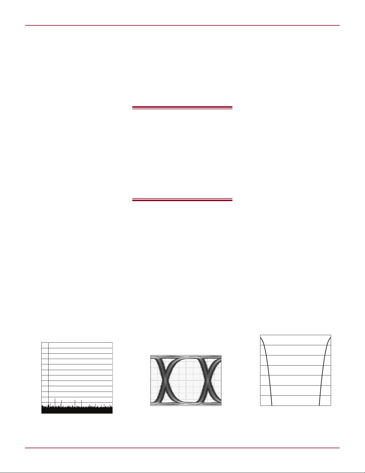
Figure 1. Typical LTC2274 performance
at 105Msps f
Linear Technology Magazine • September 2008
= 4.93MHz
IN
a. CMLOUT eye diagram 2.1GBps
Figure 2. Signal integrity of CMLOUT
b. CMLOUT Dual-Dirac BER
bathtub curve, 2.1GBps
13
Page 2

L DESIGN FEATURES
50Ω50Ω50Ω 50Ω
DATA
+
DATA
–
GND
SERIAL CML DRIVER SERIAL CML RECEIVER
1.2V TO 3.3V
16mA
CMLOUT
+
OV
DD
CMLOUT
–
50Ω
TRANSMISSION LINE
50Ω
TRANSMISSION LINE
100Ω
50Ω 50Ω
DATA
+
DATA
–
GND
SERIAL CML DRIVER SERIAL CML RECEIVER
1.4V TO 3.3V
50Ω
TRANSMISSION LINE
50Ω
TRANSMISSION LINE
16mA
CMLOUT
+
OV
DD
CMLOUT
–
50Ω50Ω
0.01µF
0.01µF
50Ω 50Ω
DATA
+
DATA
–
GND
SERIAL CML DRIVER SERIAL CML RECEIVER
1.4V TO 3.3V VTERM
16mA
CMLOUT
+
OV
DD
CMLOUT
–
50Ω
TRANSMISSION LINE
50Ω
TRANSMISSION LINE
and a P-channel device are cascaded,
the P-channel cannot pull up the signal
as fast as the N-channel can pull down.
This causes the output waveform to be
distorted, which can lead to bit errors,
and limits the speed at which LVDS
can transfer data.
The LTC2274 CML driver is implemented with only N-channel devices,
which allows faster throughput rates.
Since CML only sinks current, it has
true differential signal, which improves
signal integrity. The eye diagram and
bathtub curves of the LTC2274 are
shown in Figure 2. The eye diagram
shows very little variation cycle to
cycle of the CML logic output, and the
bathtub curve shows that total jitter
in the signal is less than 0.35UI (unit
interval). This equates into a very clean
uniform signal that can easily received
by a properly terminated receiver.
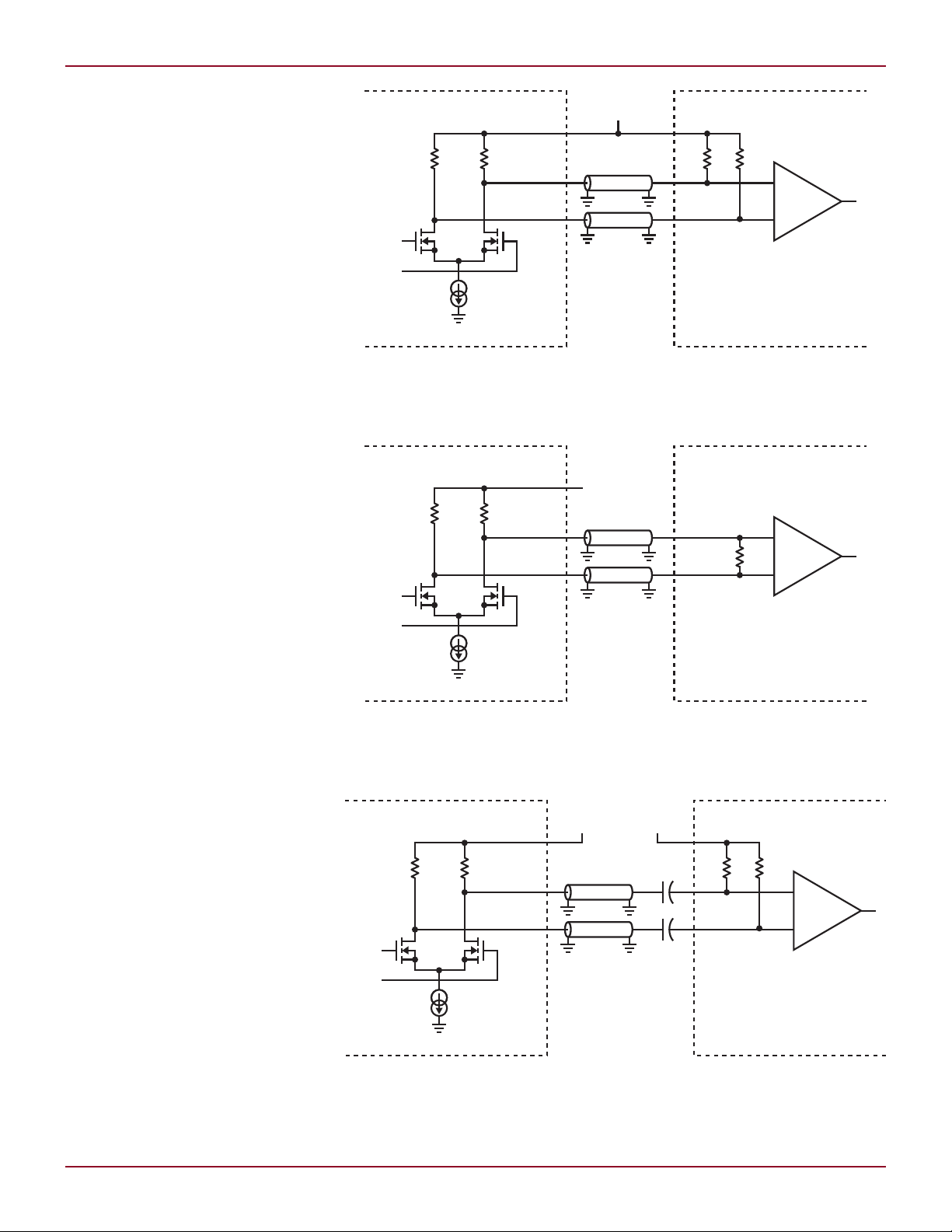
a. Recommended CML termination, directly-coupled mode
Termination of CML
CML must be terminated for proper
operation. Figure 3a shows a recommended design in which an FPGA
receiver uses internal 50Ω pull up re-
sistors for termination. These resistors
pull up to the OV
OV
must be between 1.2V and 3.3V
DD
to ensure proper operation. The signal
has a common mode voltage of OV
– 0.2V. The directly-coupled differential termination of Figure 3b may be
used in the absence of a receiver termination voltage within the required
range. In this case, the common mode
voltage is shifted down to approximately 400mV below OVDD, requiring
an OV
in the range of 1.4V to 3.3V.
DD
If the serial receiver’s common mode
input requirements are not compatible
with the directly-coupled termination
modes, the DC balanced 8B/10B
encoded data permits the addition of
DC blocking capacitors as shown in
Figure 3c. In this AC-coupled mode,
the termination voltage is determined
by the receiver’s requirements. The
coupling capacitors should be selected appropriately for the intended
operating bit-rate, usually between
1nF and 10nF. In AC coupled mode,
the output common mode voltage is
approximately 400mV below OVDD, so
the OV
14
supply voltage should be in
DD
of the LTC2274.
DD
DD
b. CML termination, directly-coupled differential mode
c. CML termination, AC-coupled mode
Figure 3. CML termination schemes
Linear Technology Magazine • September 2008
Page 3

DESIGN FEATURES L
the range of 1.4V to 3.3V. If possible,
using a lower OV
can reduce power
DD
consumption. The termination scheme
is largely based on the receiver. When
choosing the OV
voltage, refer to the
DD
receiver’s data sheet to terminate the
CML lines properly.
CML uses true double termination.
Generally, LVDS is only terminated at
the receiver, which means that any
signal reflection back to the source
reflects back to the receiver with little
attenuation. This limits the data rate
and trace length that LVDS can drive.
The truly differential nature of CML
radiates less energy than LVDS and
CMOS signals, allowing devices to be
in closer proximity to antennas, mixers or other sensitive analog front end
systems. CML also has common mode
termination. This gives CML a better
common mode behavior than LVDS.
LVDS is only terminated differentially,
which does not reject any common
mode signal that may appear on the
transmission line—another limiting
factor in LVDS signaling.
CML Power Consumption
With a constant 16mA of bias current
and a voltage swing of 800mV differential, CML logic consumes a moderate
amount of power. For an equal data
rate, CML logic consumes less total
power than PECL and LVPECL. A
single CML driver uses more power
than a single LVDS driver, but only
marginally more that the three pairs
of LVDS drivers required for a typical
LVDS serial bus.
8B/10B Encoding Makes for
Simple Connection
The 8B/10B encoding process results
in an average DC offset of zero, allowing
the data to be routed through transformers or fiber channel transceivers
that can provide isolation between
the digital and analog realm. 8B/10B
encoding also does not require a framing signal or a data clock, whereas
both are required in traditional serial
communication. 8B/10B encoding
transmits data over a single pair of
data lines, whereas a typical serial
ADC requires three or more pairs,
and a typical parallel ADC can require
more than 16 pairs.
The complexity of decoding 8B/10B
lies in the receiver. Fortunately Xilinx,
Altera and Lattice have solutions to
receive data from the LTC2274 and
decode the 8B/10B data, simplifying
the collection of 8B/10B data. Other
8B/10B decoding solutions may be
available. The FPGA required to receive
data from the LTC2274 must be able
to receive high speed serial transmissions of 2GHz or more.
Conclusion
Without sacrificing resolution or
sample rate, the LTC2274 delivers full
16-bit performance at 105Msps over
a single pair of transmission lines,
greatly simplifying layout and saving
valuable board space. This mitigates
interaction with other circuitry in
software defined radio, base station or
industrial applications which involve
many channels of an ADC routed to
one FPGA.
L
LTC35xx, continued from page 6
power synchronous boost converter
(Figure 5).
The fully integrated boost in the
LTC3586 can regulate up to a 5V output with up to 800mA from a battery
voltage as low as 3V. The regulator has
built in output disconnect making it
well-suited for USB OTG supplies or
for powering motors in printer and
camera applications. The current
mode synchronous boost is internally
compensated and operates at a fixed
2.25MHz switching frequency. Pulseskipping at low loads achieves low
noise output for driving high power
audio circuits.
I2C, Programmable
Sequencing and Easy I/O
Despite the progress in new cutting
edge features and design, one old
problem does not go away: power
supply control. Power supplies require
startup and power down sequencing,
fault detection/reporting/handling
and voltage and operating mode adjustments. Getting it all right can be
a system control nightmare depending
on the complexity and limitations of
the power supply circuits.
The LTC35xx family provides very
simple and flexible control of all essential power supply functions. The
LTC3566 and LTC3586 employ dedicated I/O control pins for enabling,
disabling and changing DC/DC
operating modes. Voltages on these
parts are fixed and set with external resistor dividers. The LTC3555,
LTC3556 and LTC3567 accommodate
either I2C control or simple I/O pins
to control the supplies. The LTC3556
provides a three-state SEQ pin to allow the power up sequence of its three
DC/DC converters to be programmed
via pin-strapping. Those parts with
I2C V
maximum V
control power-up at their
OUT
(as determined by the
OUT
FB servo point and external dividers)
when enabled via simple I/O, and
can independently reduce V
OUT
by as
much as 50% in equal 16-step increments via I2C.
All DC/DC converters in all the
PMICs discussed here can survive
an indefinite output fault. The parts
all provide a RST output and all converters are actively pulled down in
shutdown to ensure proper power-up
sequencing. The LTC3586 contains an
additional fault handing feature that
automatically powers down all DC/DC
converters whenever a valid fault is
detected. In short, the entire family
is designed for simple, flexible and
trouble-free control and operation.
Conclusion
Linear Technology’s latest PMIC
products improve the performance
and simplify the design of a wide variety of portable power management
applications. Instead of kitchen sink
alternatives with large packages,
Linear Technology offers a number of
devices with various feature mixes in
small packages. These new PMICs are
simple to use, highly integrated and
high performance, allowing for shorter
design times, greater PCB flexibility,
and better power/thermal management than traditional solutions.
L
Linear Technology Magazine • September 2008
15
 Loading...