

Application Note 106
February 2007
Instrumentation Circuitry Using RMS-to-DC Converters
RMS Converters Rectify Average Results
Jim Williams
INTRODUCTION
It is widely acknowledged that RMS (Root of the Mean
of the Square) measurement of waveforms furnishes
1
the most accurate amplitude information.
Rectify-andaverage schemes, usually calibrated to a sine wave, are
only accurate for one waveshape. Departures from this
waveshape result in pronounced errors. Although accurate,
RMS conversion often entails limited bandwidth, restricted
range, complexity and diffi cult to characterize dynamic
and static errors. Recent developments address these
issues while simultaneously improving accuracy. Figure 1
®
shows the LTC
1966/LTC1967/LTC1968 device family. Low
frequency accuracy, including linearity and gain error, is
inside 0.5% with 1% error at bandwidths extending to
500kHz. These converters employ a sigma-delta based
computational scheme to achieve their performance.
2
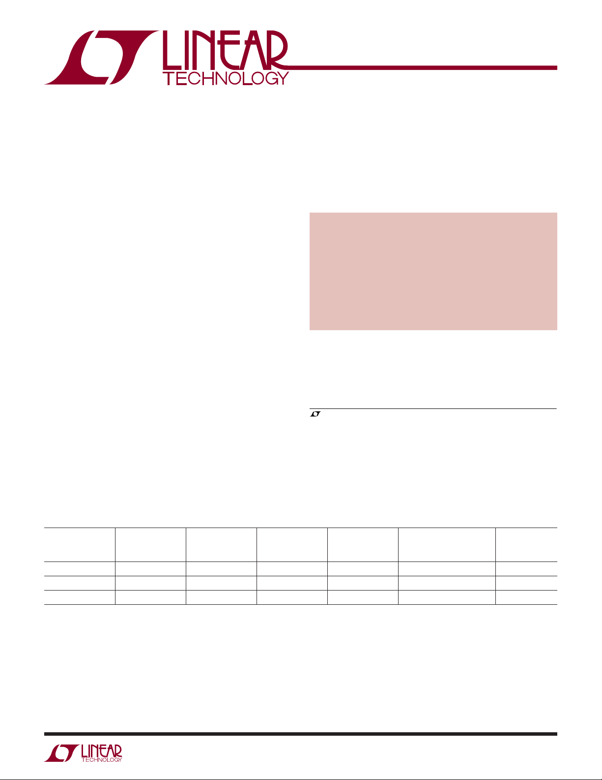
Figure 2’s pinout descriptions and basic circuits reveal an
easily applied device. An output fi lter capacitor is all that is
required to form a functional RMS-to-DC converter. Split
and single supply powered variants are shown. Such ease
of implementation invites a broad range of application;
examples begin with Figure 3.
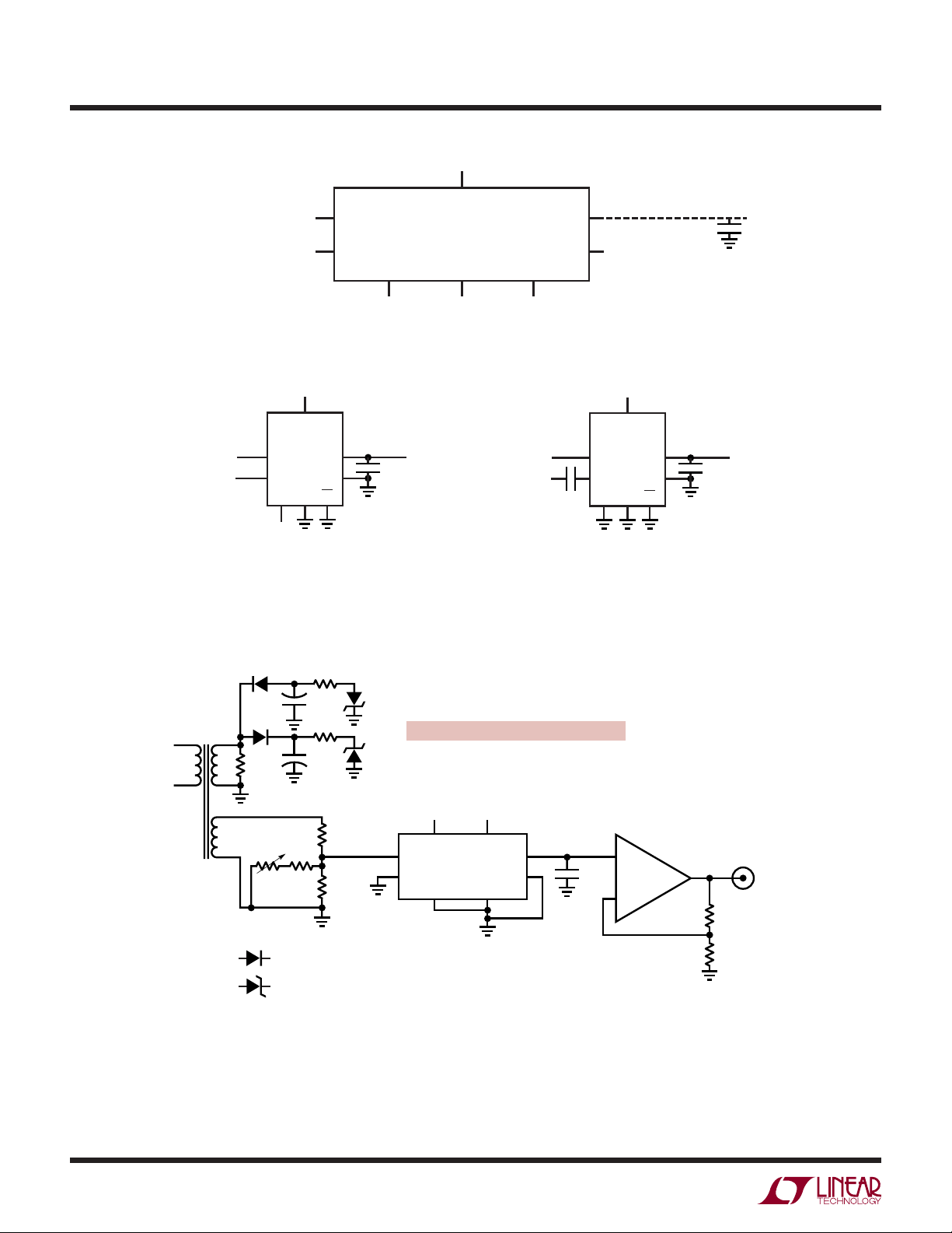
Isolated Power Line Monitor
BEFORE PROCEEDING ANY FURTHER, THE READER
IS WARNED THAT CAUTION MUST BE USED IN THE
CONSTRUCTION, TESTING AND USE OF THIS CIRCUIT.
HIGH VOLTAGE, LETHAL POTENTIALS ARE PRESENT IN
THIS CIRCUIT. EXTREME CAUTION MUST BE USED IN
WORKING WITH, AND MAKING CONNECTIONS TO, THIS
CIRCUIT. REPEAT: THIS CIRCUIT CONTAINS DANGEROUS, HIGH VOLTAGE POTENTIALS. USE CAUTION.
Figure 3’s AC power line monitor has 0.5% accuracy over
a sensed 90VAC to 130VAC input and provides a safe, fully
isolated output. RMS conversion provides accurate reporting of AC line voltage regardless of waveform distortion,
which is common.
, LT, LTC and LTM are registered trademarks of Linear Technology Corporation.
All other trademarks are the property of their respective owners.
1
See Appendix A, “RMS-to-DC Conversion” for complete discussion of
RMS measurement.
2
Appendix A details sigma-delta based RMS-to-DC converter operation.
LINEARITY
PART NUMBER
LTC1966 0.02/0.15 0.1/0.3 6 800 2.7 ±5 170
LTC1967 0.02/0.15 0.1/0.3 200 4MHz 4.5 5.5 390
LTC1968 0.02/0.15 0.1/0.3 500 15MHz 4.5 5.5 2.3mA
Figure 1. Primary Differences in RMS to DC Converter Family are Bandwidth and Supply Requirements.
All Devices Have Rail-to-Rail Differential Inputs and Output
ERROR
TYP/MAX (%)
CONVERSION
GAIN ERROR
TYP/MAX (%)
1% ERROR
BANDWIDTH
(kHz)
3dB ERROR
BANDWIDTH
(kHz)
SUPPLY VOLTAGE I
MIN(V) MAX(V)
AN106-1
SUPPLY
MAX (µA)
an106f
Application Note 106
POSITIVE SUPPLY
2.7V TO 5.5V
DEPENDING ON DEVICE CHOICE
DIFFERENTIAL
MAX COMMON MODE
INPUTS.
RANGE = ±V SUPPLY.
MAX DIFFERENTIAL = 1V.
MINIMUM INPUT = 5mV
INPUT 1
INPUT 2
±5V Supplies, Differential, DC-Coupled
RMS-to-DC Converter
5V
V
DD
DC + AC
INPUTS
(1V
DIFFERENTIAL)
PEAK
LTC1966
IN1
IN2
SS
–5V
V
OUT RTN
GND ENV
OUT
Figure 2. RMS Converter Pin Functions (Top) and Basic Circuits (Bottom).
Pin Descriptions are Common to All Devices, with Minor Differences
SET HIGH TO
SHUT DOWN
C
AVE
1µF
LTC1966
LTC1967
LTC1968
LTC1966 ONLY.
0V TO –5V
SUPPLY
DC OUTPUT
= 85kΩ
Z
O
+V
–V*ENABLE
DIFFERENTIAL)
OUTPUT OUTPUT
OUTPUT RETURN
GND
POWER
GROUND
OUTPUT TO FILTER CAPACITOR
OUTPUT REFERRED
TO THIS PIN.
NORMALLY GROUNDED
*NO –V PIN ON THE LTC1967/LTC1968
5V Single Supply, Differential, AC-Coupled
RMS-to-DC Converter
5V
V
DD
AC INPUTS
(1V
PEAK
0.1µF
LTC1966
V
IN1
IN2
C
C
SS
OUT RTN
GND ENV
OUT
AN106 F02
C
1µF
AVE
DC OUTPUT
= 85kΩ
Z
O
LINE INPUT
90VAC
TO 140VAC
T1
145
BIAS SUPPLY
100Ω
A
1W
6
ISOLATED LINE SENSE
7
B
1k
8
120VAC
TRIM
T1 = TAMURA-PAN MAG 3FS-212
*1% METAL FILM RESISTOR
1µF = WIMA MKS-2
1k
100µF
+
1k
+
100µF
100Ω
1W
0.25%
100Ω
10Ω
0.25%
= 1N4148
= 1N4689 5.1V
–5V
5V
DANGER! Lethal Potentials Present—See Text
5V –5V
+V –V
IN1 OUT
IN2
EN GND
C1
LTC1966
OUT RTN
RMS CONVERTER
1µF
+
A1
®
1006
LT
–
RMS OUT
0.9V TO 1.4V =
90VAC TO 140VAC
100k*
100k*
AN106 F03
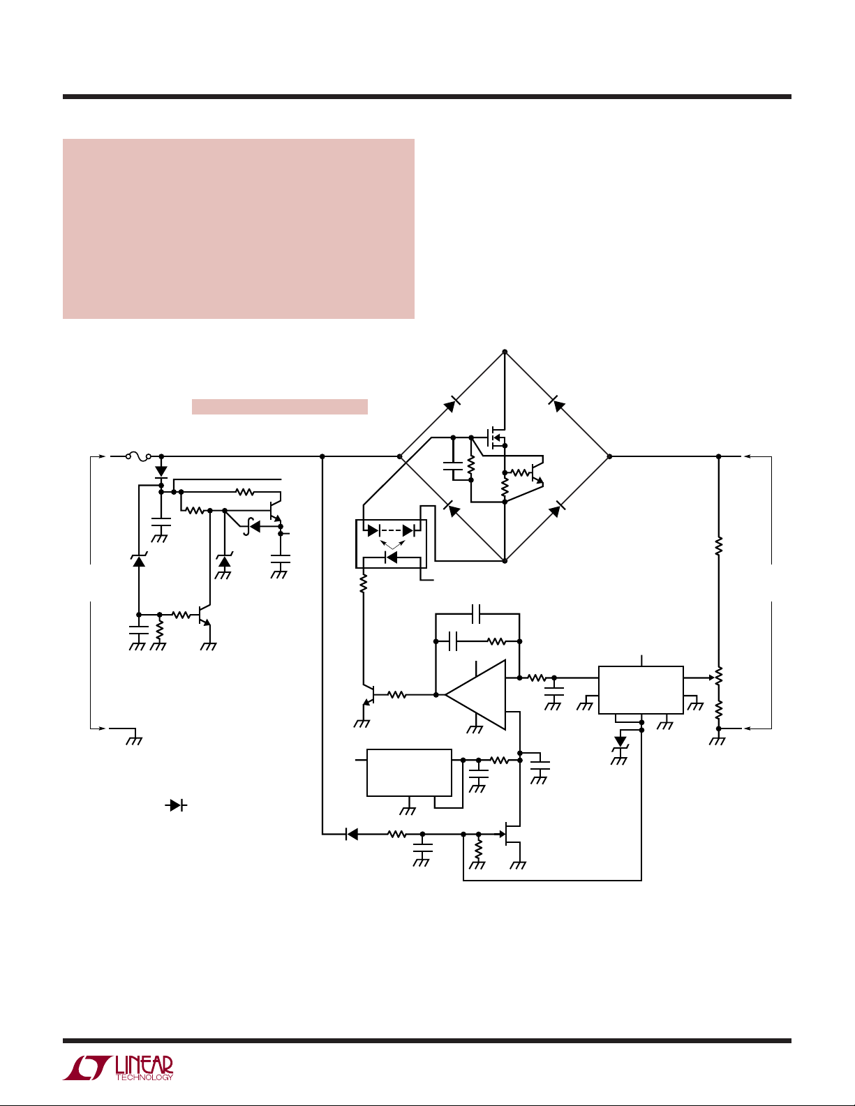
Figure 3. Isolated Power Line Monitor Senses Via Transformer with 0.5% Accuracy Over 90VAC to 130VAC Input.
Secondary Loading Optimizes Transformer Voltage Conversion Linearity
AN106-2
an106f
Application Note 106
The AC line voltage is divided down by T1’s ratio. An isolated
and reduced potential appears across T1’s secondary B,
where it is resistively scaled and presented to C1’s input.
Power for C1 comes from T1’s secondary A, which is
rectifi ed, fi ltered and zener regulated to DC. A1 takes gain
and provides a numerically convenient output. Accuracy
is increased by biasing T1 to an optimal loading point,
facilitated by the relatively low resistance divider values.
Similarly, although C1 and A1 are capable of single supply
operation, split supplies maintain symmetrical T1 loading.
The circuit is calibrated by adjusting the 1k trim for 1.20V
output with the AC line set at 120VAC. This adjustment is
made using a variable AC line transformer and a well fl oated
(use a line isolation transformer) RMS voltmeter.
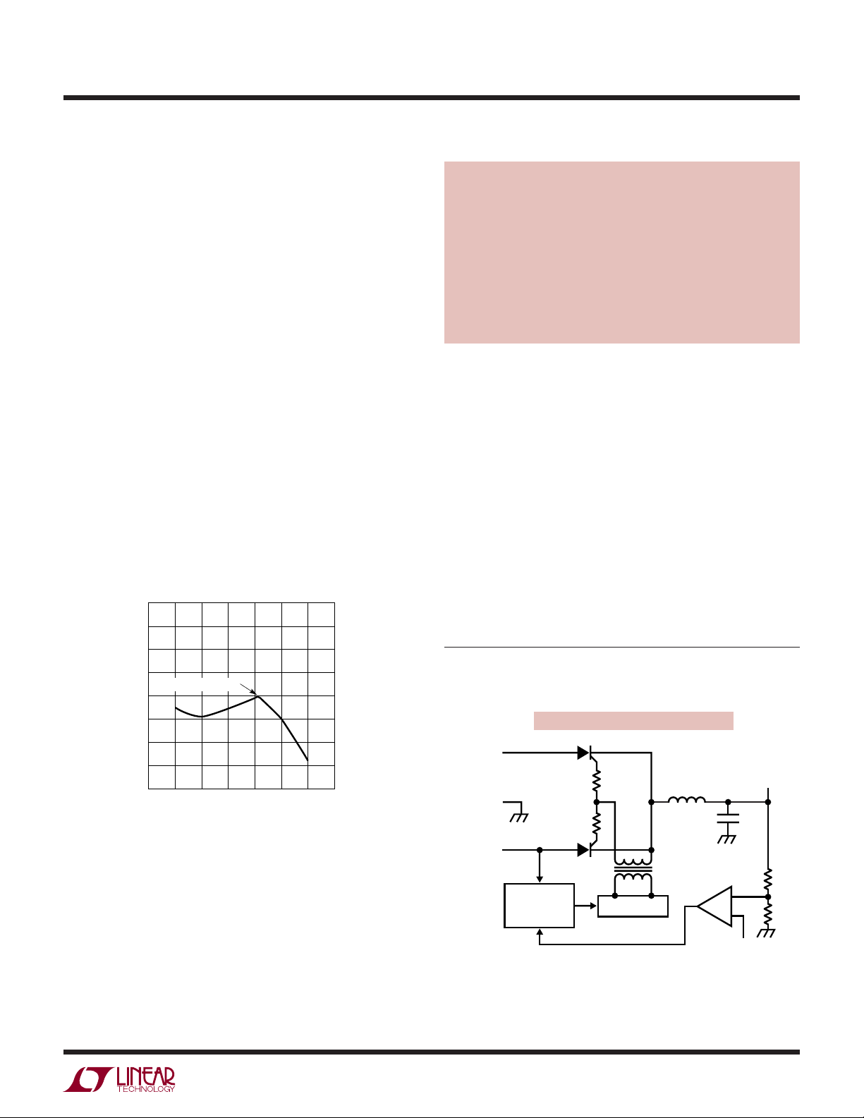
F
igure 4’s error plot shows 0.5% accuracy from 90VAC
3
to 130VAC, degrading to 1.4% at 140VAC. The benefi cial
effect of trimming at 120VAC is clearly evident; trimming at full scale would result in larger overall error,
primarily due to non-ideal transformer behavior. Note
that the data is specifi c to the transformer specifi ed.
Substitution for T1 necessitates circuit value changes
and recharacterization.
2.0
1.5
1.0
0.5
120VAC TRIM POINT
0
–0.5
–1.0
RMS OUTPUT READING ERROR (%)
–1.5
–2.0
90 100 120
Figure 4. Error Plot for Isolated Line Monitor Shows 0.5%
Accuracy from 90VAC to 130VAC, Degrading to 1.4% at 140VAC.
Transformer Parasitics Account for Almost All Error
110
RMS INPUT VOLTAGE (V)
130 140
AN106 F04
Fully Isolated 2500V Breakdown,
Wideband RMS-to-DC Converter
NOTE: BEFORE PROCEEDING ANY FURTHER, THE
READER IS WARNED THAT CAUTION MUST BE USED
IN THE CONSTRUCTION, TESTING AND USE OF THIS
CIRCUIT. HIGH VOLTAGE, LETHAL POTENTIALS ARE
PRESENT IN THIS CIRCUIT. EXTREME CAUTION MUST
BE USED IN WORKING WITH, AND MAKING CONNECTIONS TO, THIS CIRCUIT. REPEAT: THIS CIRCUIT
CONTAINS DANGEROUS, HIGH VOLTAGE POTENTIALS.
USE CAUTION.
Accurate RMS amplitude measurement of SCR chopped
AC line related waveforms is a common requirement. This
measurement is complicated by the SCR’s fast switching
of a sine wave, introducing odd waveshapes with high
frequency harmonic content. Figure 5’s conceptual SCRbased AC/DC converter is typical. The SCRs alternately
chop the 220VAC line, responding to a loop enforced,
phase modulated trigger to maintain a DC output. Figure
6’s waveforms are representative of operation. Trace A is
one AC line phase, trace B the SCR cathodes. The SCR’s
irregularly shaped waveform contains DC and high frequency harmonic, requiring wideband RMS conversion
for measurement. Additionally, for safety and system
interface considerations, the measurement must be fully
isolated.
3
See Appendix B, “AC Measurement and Signal Handling Practice,” for
recommendations on RMS voltmeters and other AC measurement related
gossip.
DANGER! Lethal Potentials Present—See Text
220VAC
INPUT
NEUTRAL
220VAC
AC LINE SYNC
AND PHASE
MODULATION
TRIGGER
DC
OUTPUT
AN106 F05
REF
Figure 5. Conceptual AC/DC Converter is Typical of SCR-Based
Confi gurations. Feedback Directed, AC Line Synchronized
Trigger Phase Modulates SCR Turn-On, Controlling DC Output
an106f
AN106-3
Application Note 106
A = 100V/DIV
B = 50V/DIV
ON 170 VDC
LEVEL
1ms/DIV
Figure 6. Typical SCR-Based Converter Waveforms Taken at AC
Line (Trace A) and SCR Cathodes (Trace B). SCR’s Irregularly
Shaped Waveform Contains DC and High Frequency Harmonic,
Requiring Wideband RMS Converter for Measurement
AN106 F06
Figure 7 provides isolated power and data output paths to
an RMS-to-DC converter, permitting safe, wideband, digital
output RMS measurement. A pulse generator confi gured
comparator combines with Q1 and Q2 to drive T1, resulting
in isolated 5V power at T1’s rectifi ed, fi ltered and zener
regulated output. The RMS-to-DC converter senses either
135VAC or 270VAC full-scale inputs via a resistive divider.
The converter’s DC output feeds a self-clocked, serially
interfaced A/D converter; optocouplers convey output data
across the isolation barrier. The LTC6650 provides a 1V
reference to the A/D and biases the RMS-to-DC converter’s
inputs to accommodate the voltage divider’s AC swing.
Calibration is accomplished by adjusting the 20k trim while
noting output data agreement with the input AC voltage.
Circuit accuracy is within 1% in a 200kHz bandwidth.
0.001µF
PULSE GENERATOR
1N4148
1k
220k
–
LT1671
+
DRIVER
1k
750k
750k
750k
DATA
ISOLATORS
SCK
DATA
OUTPUTS
SDO
5VPOWER
1k
100Ω
Q1
2N2369
5V
ISOLATION/POWER
Q2
ZTX-749
2Ω
3
1
6
4
T1
TRANSFORMER
2500V BREAKDOWN
ISOLATION BARRIER
5V
5V
ISOLATED POWER SUPPLY
1N5817
1N4148
4.7k
4.7k
1N4689
5.1V
5V ISO
A/D RMS CONVERTER
5V ISO
+V
SCK V
LTC2400
SDO
FOGND CS
5V ISO
+
5V ISO
+
100µF
DANGER! Lethal Potentials Present—See Text
5V ISO
–
IN
REF
10µF
5V ISO
LT1006
+
1µF
†
5V ISO
+V
OUT IN1
LTC1967
OUT RTN IN2
GND
EN
CALIBRATE
20k
0.1µF
182k*
182k*
1k*
INPUT
135VAC
OR
270VAC
FULL SCALE
ISOLATORS = AGILENT-HCPL-2300-010
T1 = BI TECHNOLOGIES HM-41-11510
* = 1% METAL FILM RESISTOR
† = WIMA MKS-2
= CIRCUIT COMMON
= AC LINE GROUND
1µF
400mV
REFERENCE
LT6650
+
OUT
–
15k*
FB
10k*
1µF
1VDC
AN106 F07
Figure 7. Isolated RMS Converter Permits Safe, Digital Output, Wideband RMS Measurement. T1-Based Circuitry Supplies Isolated
Power. RMS-to-DC Converter Senses High Voltage Input via Resistive Divider. A/D Converter Provides Digital Output Through
Optoisolators. Accuracy is 1% in 200kHz Bandwidth
AN106-4
an106f
Application Note 106
Low Distortion AC Line RMS Voltage Regulator
NOTE: BEFORE PROCEEDING ANY FURTHER, THE
READER IS WARNED THAT CAUTION MUST BE USED
IN THE CONSTRUCTION, TESTING AND USE OF THIS
CIRCUIT. HIGH VOLTAGE, LETHAL POTENTIALS ARE
PRESENT IN THIS CIRCUIT. EXTREME CAUTION MUST
BE USED IN WORKING WITH, AND MAKING CONNECTIONS TO, THIS CIRCUIT. REPEAT: THIS CIRCUIT
CONTAINS DANGEROUS, HIGH VOLTAGE POTENTIALS.
USE CAUTION.
DANGER! Lethal Potentials Present—See Text
1.5A
AC
SB
HIGH
UNREGULATED
AC LINE
INPUT
0.22µF
AC
LOW
+V REGULATORS
470k
0.47µF
1N5281B
200V
200k
200k
HEAT SINK IRF-840
*1% METAL FILM RESISTOR
OPTODRIVER = TOSHIBA TLP190B
= 1N4005
Q3
2N5210
100k
1N4690
5.6V
BAT85
OVERVOLTAGE
PROTECTION
170V
Q4
MPSA42
5V
0.1µF
2N3440
10k
2W
ISOLATED
GATE BIAS
5.6k
Q1
REFERENCE
0.4V OUT5V IN
LT6650
GND
1M
Almost all AC line voltage regulators rely on some form of
waveform chopping, clipping or interruption to function.
This is effi cient, but introduces waveform distortion, which
is unacceptable in some applications. Figure 8 regulates
the AC line’s RMS value within 0.25% over wide input
swings and does not introduce distortion. It does this by
continuously controlling the conductivity of a series pass
MOSFET in the AC lines path. Enclosing the MOSFET in
a diode bridge permits it to operate during both AC line
polarities.
AC SERIES PASS
AND CURRENT LIMIT
0.03µF
FB
170V
1µF
0.22µF
0.1µF
5V
LT1077
430k
0.7Ω
A1
100k
Q2
IRF-840
10k
CONTROL
AMPLIFIER
22k
–
+
330k
1µF
10k
Q5
2N4393
Q6
2N3904
2.2µF
MYLAR
RMS-TO-DC CONVERTER
C1
OUT
1µF
OUT RTN
1N4689
5.1V
5V
+V
LTC1966
–VEN
GND
FEEDBACK
IN1
IN2
SENSE
AC HIGH
1k
AC LOW
2.2M*
REGULATED
105VAC
TO 120VAC
ADJUST
7.32k*
OUTPUT
VAC
AN106 F08
SOFT-START/–V
BIAS
Figure 8. Adjustable AC Line Voltage Regulator Introduces No Waveform Distortion. Line Voltage RMS Value is Sensed and
Compared to a Reference by A1. A1 Biases Photovoltaic Optocoupler via Q1, Setting Q2-Diode Bridge Conductivity and Closing a
Control Loop. VIN Must be ≥2V Above V
to Maintain Regulation
OUT
an106f
AN106-5

Application Note 106
The AC line voltage is applied to the Q2-diode bridge. The
Q2-diode bridge output is sensed by a calibrated variable
voltage divider which feeds C1. C1’s output, representing
the regulated lines RMS value, is routed to control amplifi er A1 and compared to a reference. A1’s output biases
Q1, controlling drive to a photovoltaic optoisolator. The
optoisolator’s output voltage provides level-shifted bias
to diode bridge enclosed Q2, closing a control loop which
regulates the output’s RMS voltage against AC line and
load shifts. RC components in A1’s local feedback path
stabilize the control loop. The loop operates Q2 in its
linear region, much like a common low voltage DC linear
regulator. The result is absence of introduced distortion
at the expense of lost power. Available output power is
constrained by heat dissipation. For example, with the
output adjustment set to regulate 10V below the normal
input, Q2 dissipates about 10W at 100W output. This fi gure
can be improved upon. The circuit regulates for V
above V
dropout as V
, but operation in this region risks regulation
OUT
varies.
IN
≥ 2V
IN
Circuit details include JFET Q5 and associated components.
The passive components associated with Q5’s gate form
a slow turn-on negative supply for C1. They also provide
gate bias for Q5. Q5, a soft-start, prevents abrupt AC power
application to the output at start-up. When power is off,
Q5 conducts, holding A1’s “+” input low. When power
is applied, A1 initially has a zero volt reference, causing
the control loop to set the output at zero. As the 1MΩ
0.22µF combination charges, Q5’s gate moves negative,
causing its channel conductivity to gradually decay. Q5
ramps off, A1’s positive input moves smoothly towards
the LT6650’s 400mV reference, and the AC output similarly
ascends towards its regulation point. Current sensor Q6,
measuring across the 0.7Ω shunt, limits output current
to about 1A. At normal line inputs (90VAC to 135VAC) Q4
supplies 5V operating bias to the circuit. If line voltage
rises beyond this point, Q3 comes on, turning off Q4 and
shutting down the circuit.
X1000 DC Stabilized Millivolt Preamplifi er
The preceding circuits furnish high level inputs to the RMS
converter. Many applications lack this advantage and some
form of preamplifi er is required. High gain pre-amplifi cation
for the RMS converter requires more attention than might
be supposed. The preamplifi er must have low offset error
because the RMS converter (desirably) processes DC as
legitimate input. More subtly, the preamplifi er must have
far more bandwidth than is immediately apparent. The
amplifi ers –3db bandwidth is of interest, but its closed
loop 1% amplitude error bandwidth must be high enough
to maintain accuracy over the RMS converter’s 1% error
passband. This is not trivial, as very high open-loop gain
at the maximum frequency of interest is required to avoid
inaccurate closed-loop gain.
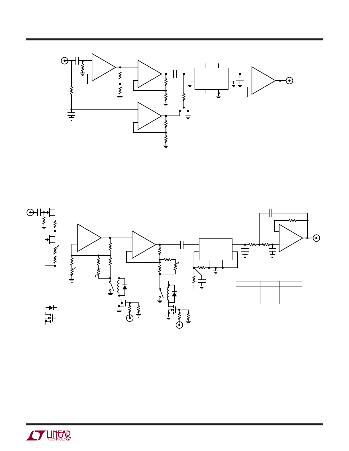
Figure 9 shows an x1000 preamplifi er which preserves the
LTC1966’s DC-6kHz 1% accuracy. The amplifi er may be
either AC or DC coupled to the RMS converter. The 1mV
full-scale input is split into high and low frequency paths.
AC coupled A1 and A2 take a cascaded, high frequency
gain of 1000. DC coupled, chopper stabilized A3 also has
X1000 gain, but is restricted to DC and low frequency by
its RC input fi lter. Assuming the switch is set to “DC + AC,”
high and low frequency path information recombine at the
RMS converter. The high frequency paths 650kHz –3db
response combines with the low frequency sections microvolt level offset to preserve the RMS converters DC-6kHz
1% error. If only AC response is desired, the switch is set
to the appropriate position. The minimum processable
input, set by the circuits noise fl oor, is 15µV.
Wideband Decade Ranged X1000 Preamplifi er
The LTC1968, with a 500kHz, 1% error bandwidth, poses
a signifi cant challenge for an accurate preamplifi er, but
Figure 10 meets the requirement. This design features
decade ranged gain to X1000 with a 1% error bandwidth
beyond 500kHz, preserving the RMS converters 1% error bandwidth. Its 20µV noise fl oor maintains wideband
performance at microvolt level inputs.
Q1A and Q1B form a low noise buffer, permitting high
impedance inputs. A1 and A2, both gain switchable, take
cascaded gain in accordance with the fi gure’s table. The
gains are settable via reed relays controlled by a 2-bit code.
A2’s output feeds the RMS converter and the converter’s
output is smoothed by a Sallen-Keys active fi lter. The
circuit maintains 1% error over a 10Hz to 500kHz bandwidth at all gains due to the preamplifi ers –3db, 10MHz
bandwidth. The 10Hz low frequency restriction could be
eliminated with a DC stabilization path similar to Figure
9’s but its gain would have to be switched in concert with
the A1-A2 path.
an106f
AN106-6
Application Note 106
INPUT
0mV TO 1mV
1µF
100pF
HIGH FREQUENCY PATH AC/DC SUMMATION RMS CONVERTER
+
A1
1M
LT1122
–
LOW FREQUENCY/DC PATH
*1% METAL FILM RESISTOR
1µF = WIMA MKS-2
10k*
536Ω*1M
+
A2
LT1222
–
+
A3
LTC1050
–
1µF
10k*
200Ω*
DC + AC
1M*
1k*
100k
5V –5V
+V –V
IN1
EN GND
AC
RMS STAGE INPUT COUPLING
LTC1966
OUT
OUT RTNIN2
1µF
+
LT1077
–
OUTPUT
A4
0V TO 1V
AN106 F09
Figure 9. X1000 Preamplifi er Allows 1mV Full-Scale Sensitivity RMS-to-DC Conversion. Input Splits Into High and Low Frequency
Amplifi er Paths, Recombining at RMS Converter. Amplifi er’s –3dB, 650kHz Bandwidth Preserves RMS-to-DC Converter’s 6kHz, 1%
Error Bandwidth. Noise Floor is 15µV
INPUT BUFFER OUTPUT FILTER
5V
1µF
INPUT
Q1A
1M
100Ω
SWITCHED GAIN AMP
A = 1, 100
+
10k
200k
–
A1
LT1227
A = 100
TRIM
Q1B
ZERO
100Ω
50Ω
A = 1
–5V
TRIM
Q1 = 2N6485. GROUND CASE
*1% METAL FILM RESISTOR
RELAYS = COTO-COIL 800-05-001
10µF, 1µF = WIMA MKS-2
= 1N4148
= VN2222L
22Ω
100Ω
499Ω*
5.62Ω*
5V
SWITCHED GAIN AMP
+
A2
LT1227
–
1M20k
S1
A = 1, 10
750Ω*
470Ω
90.9Ω*
5V
1k
1µF
A = 10
TRIM
S2
20k
10k
5V
1M
RMS CONVERTER
5V
+V
IN1
LTC1968
EN GND
10k
0.1µF
OUT
OUT RTNIN2
5.62k* 24.9k*
S1
S2
LO
LO
LO
HI
HI
LO
HI
HI
*SET ZERO ADJUSTMENT FOR A2
OUTPUT = 0 VDC WITH INPUT GROUNDED
AND S1, S2 HIGH BEFORE TRIMMING
GAIN
10
100
1000
1
10µF
1µF10µF
FS OUTPUT
1V
0.1V
0.01V
0.001V
43k
–
A3
LT1077
+
TRIM NOTES*
TRIM A = 1
TRIM A = 10
TRIM A = 100
NO TRIM
OUTPUT
AN106 F10
Figure 10. Switched Gain 10MHz (–3dB) Preamplifi er Preserves LTC1968’s 500kHz, 1% Error Bandwidth. Decade Ranged Gains
(See Table) Allow 1mV Full Scale with 20µV Noise Floor. JFET Input Stage Presents High Input Impedance. AC Coupling, 3rd Order
Sallen-Key Filter Maintains 1% Accuracy Down to 10Hz
an106f
AN106-7
Application Note 106
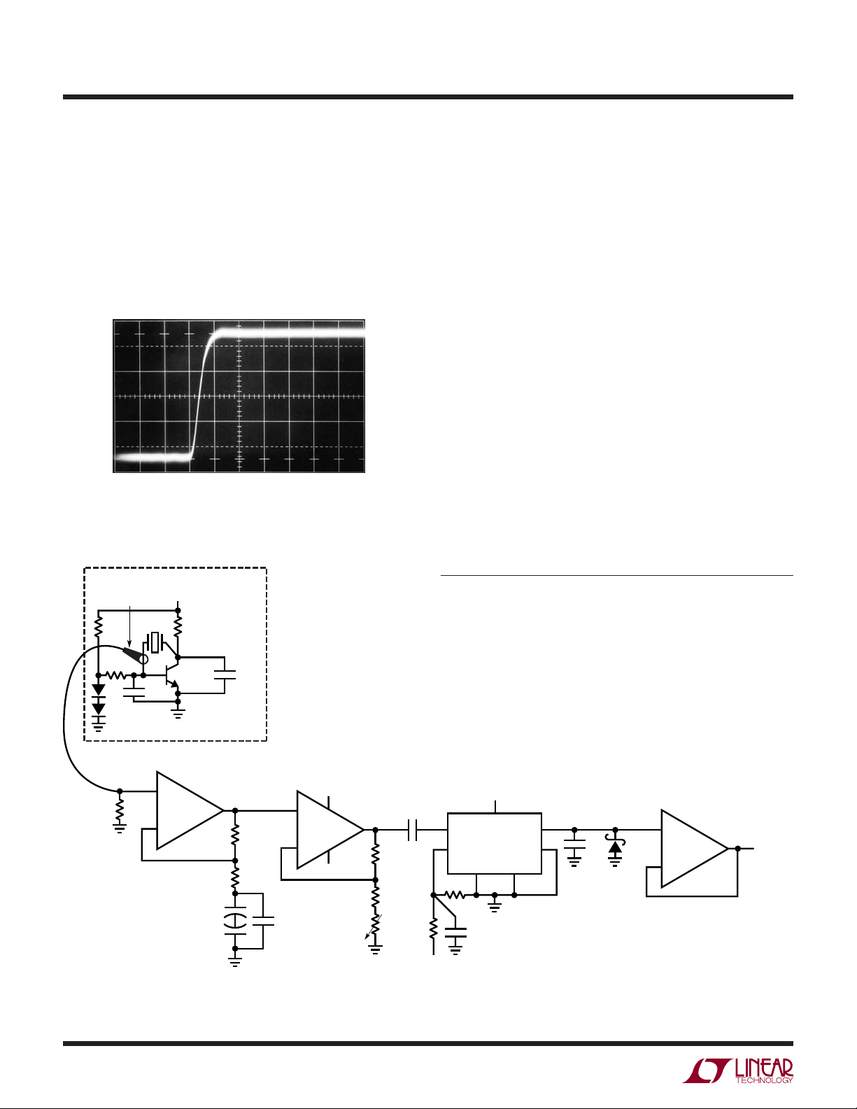
Figure 11 shows preamplifi er response to a 1mV input
step at a gain of X1000. A2’s output is singularly clean,
with trace thickening in the pulse fl at portions due to the
20µV noise fl oor. The 35ns risetime indicates a 10MHz
bandwidth.
To calibrate this circuit fi rst set S1 and S2 high, ground
the input and trim the “zero” adjustment for zero VDC at
A2’s output. Next, set S1 and S2 low, apply a 1V, 100kHz
input, and trim “A = 1” for unity gain, measured at the
200mV/DIV
50ns/DIV
Figure 11. Figure 10’s A2 Output Responds to a 1mV Input Step
at X1000 Gain. 35ns Risetime Indicates 10MHz Bandwidth. Trace
Thickening in Pulse Flat Portions Represents Noise Floor
TEKTRONIX CT-2
CURRENT PROBE
1mV/mA
1.5V
AN106 F11
circuit output, in accordance with the table in the fi gure.
Continue this procedure for the remaining three gains
given in the table. A good way to generate the accurate
low level inputs required is to set a 1.00VAC level and
divide it down with a high grade 50Ω attenuator such
as the Hewlett Packard 350D or the Tektronix 2701. It is
prudent to verify the attenuator’s output with a precision
RMS voltmeter.
4
Wideband, Isolated, Quartz Crystal RMS Current
Measurement
Quartz crystal RMS operating current is critical to longterm stability, temperature coeffi cient and reliability. Accurate determination of RMS crystal current, especially
in low power types, is complicated by the necessity to
minimize introduced parasitics, particularly capacitance,
which corrupt crystal operation. Figure 12, a form of
Figure 10’s wideband amplifi er, combines with a commercially available closed core current probe to permit
the measurement. An RMS-to-DC converter supplies
the RMS value. The quartz crystal test circuit shown in
dashed lines exemplifi es a typical measurement situation. The Tektronix CT-2 current probe monitors crystal
4
See Appendix B for recommendations on RMS voltmeters.
4.3k
330k
1N4148s
100kHz
50Ω*
680pF
+
LT1227
–
10k
Q1
2N3904
A1
PRE-AMPLIFIER
+
47µF
47µF
150pF
A = 1000
499Ω*
5.62Ω*
+
CRYSTAL
OSCILLATOR
TEST CIRCUIT
+
A2
LT1227
–
0.1µF
5V
–5V
750Ω*
64.9Ω*
20Ω
1mA
TRIM
1µF
10k
IN1
10k
5V
RMS CONVERTER
5V
+V
LTC1968
OUT RTNIN2
EN GND
0.1µF
OUT
1µF 1N5712
*0.25% METAL FILM RESISTOR
+
LT1077
–
AN106 F12
OUTPUT
0 – 1V =
0 – 1mA
A3
Figure 12. Figure 10’s Wideband Amplifi er Adapted for Isolated RMS Current Measurement of Quartz Crystal Current. FET Input Buffer
is Deleted; Current Probe’s 50Ω Impedance Allows Direct Connection to A1. Current Probe Provides Minimal Crystal Loading
in Oscillator Test Circuit
an106f
AN106-8

Application Note 106
current while introducing minimal parasitic loading (see
Figure 14). The probe’s 50Ω termination allows direct
connection to A1—Figure 10’s FET buffer is deleted. Additionally, because quartz crystals are not common below
4kHz, A1’s gain does not extend to low frequency.
Figure 13 shows results. Crystal drive, taken at Q1’s collector (trace A), causes a 25µA RMS crystal current which
is represented at the RMS-to-DC converter input (trace B).
The trace enlargement is due to the preamplifi er’s 5µA
RMS equivalent noise contribution.
A = 0.5V/DIV
B = 50mA/DIV
2ms/DIV
Figure 13. Crystal Voltage (Trace A) and Current (Trace B) for
Figure 12’s Test Circuit. 25µA RMS Crystal Current Measurement
Includes Preamplifi er 5µA RMS Noise Floor Contribution
PARAMETER CT-1 CT-2
Sensitivity 5mV/mA 1mV/mA
Accuracy 3% 3%
Low Frequency Additional
1% Error BW*
–3dB Bandwidth 25kHz to 1GHz 1.2kHz to 200MHz
Noise Floor with Amplifi er
Shown*
Capacitive Loading 1.5pF 1.8pF
Insertion Impedance at
10MHz
*As measured. Not vendor specifi ed
Figure 14. Relevant Specifi cations of Two Tektronix Current
Probes. Primary Trade-Off is Low Frequency Error and
Sensitivity. Noise Floor is Due to Amplifi er Limitations
98kHz 6.4kHz
1µA RMS 5µA RMS
1Ω 0.1Ω
AN106 F13
Figure 14 details characteristics of two Tektronix closed
core current probes. The primary trade-off is low frequency
error versus sensitivity. There is essentially no probe
noise contribution and capacitive loading is notably low.
Circuit calibration is achieved by putting 1mA RMS current
through the probe and adjusting the indicated trim for a
1V circuit output. To generate the 1mA, drive a 1k, 0.1%
5
resistor with 1V
RMS
.
AC Voltage Standard with Stable Frequency and Low
Distortion
Figure 15 utilizes the RMS-to-DC converter’s stability in an
AC voltage standard. Initial circuit accuracy is 0.1% and
long-term (6 months at 20°C to 30°C) drift remains within
that fi gure. Additionally, the 4kHz operating frequency is
within 0.01% and distortion inside 30ppm.
A1 and its power buffer A3 sense across a bridge composed
of a 4kHz quartz crystal and an RC impedance in one arm;
resistors and an LED driven photocell comprise the other
arm. A1 sees positive feedback at the crystals 4kHz resonance, promoting oscillation. Negative feedback, stabilizing oscillation amplitude, occurs via a control path which
includes an RMS-to-DC converter and amplitude control
amplifi er, A5. A5 acts on the difference between A3’s RMS
converted output and the LT1009 voltage reference. Its
output controls the LED driven photocell to set A1’s negative
feedback. RC components in A5’s feedback path stabilize the
control loop. The 50k trim sets the optically driven resistor’s
value to the point where lowest A3 output distortion occurs
while maintaining adequate loop stability.
Normally the bridge’s “bottom” would be grounded. While
this connection will work, it subjects A1 to common mode
swings, increasing distortion due to A1’s fi nite common
mode rejection versus frequency. A2 eliminates this concern by forcing the bridges mid-points, and hence common
mode voltage, to zero while not infl uencing desired circuit
operation. It does this by driving the bridge “bottom” to
force its input differential to zero. A2’s output swing is
180° out of phase with A3’s circuit output. This action
eliminates common mode swing at A1, reducing circuit
output distortion by more than an order of magnitude. Figure 16 shows the circuits 1.414V
RMS
(2.000V
PEAK
) output
in trace A while trace B’s distortion constituents include
noise, fundamental related residue and 2F components.
The 4kHz crystal is a relatively large structure with very
high Q factor. Normally, it would require more than 30
seconds to start and arrive at full regulated amplitude.
This is avoided by inclusion of the Q1-LTC201 switch
circuitry. At start-up A5’s output goes high, biasing Q1.
Q1’s collector goes low, turning on the LTC201. This sets
A1’s gain abnormally high, increasing bridge drive and
5
This measurement technique has been extended to monitor 32.768kHz
“watch crystal” sub-microampere operating currents. Contact the author
for details.
an106f
AN106-9

Application Note 106
CRYSTAL BRIDGE BRIDGE AMPLIFIER
430pF
47k
50k
–5V
DISTORTION
TRIM
1k
1/4 LTC201
START-UP
+
LT1792
–
A1
1k
4kHz
J
–
A2
LT1792
+
CUT
560k
COMMON
MODE
SUPPRESSION
AMPLIFIER
5V
470Ω
2N3904
4kHz
OUTPUT
1.414V
39k
5V
A5
CONTROL
10µF
RMS
+
AN106 F15
–5V
2.5k*
LT1009
–
LT1077
+
2.5V
A4
RMS-TO-DC CONVERTER
A3
LT1010
5V
1M
Q1
510k
100k
1k*
909Ω*
200Ω
OUTPUT
SET
*IRC-CAR-6 1% RESISTOR
GROUND CRYSTAL CASE
5V
+
V
IN1 OUT
LTC1966
IN2
EN RTN GND V
= 1N4148
–
–5V
= SILONEX NSL-32SR3
1µF
28k*
100k*
–
LT1006
+
AMPLITUDE
AMPLIFIER
Figure 15. Quartz Stabilized Sine Wave Output AC Reference Has 0.1% Long-Term Amplitude Stability. Frequency Accuracy is 0.01%
with <30ppm Distortion. Positive Feedback Around A1 Causes Oscillation at Crystal’s Resonance. A5, Acting on A3’s RMS Amplitude,
Supplies Negative Feedback to A1 via Bridge Network, Stabilizing RMS Output Amplitude. Optocoupler Minimizes Feedback Induced
Distortion. Q1 Closes Switch During Start-Up, Ensuring Rapid Oscillation Build-Up
the trim for minimal output distortion as measured on a
distortion analyzer. Note that the absolute lowest level
A = 2V/DIV
of distortion coincides with the point where control loop
gain is just adequate to maintain oscillation. As such,
fi nd this point and retreat from it into the control loop’s
B = 30ppm
DISTORTION
active region. This necessitates giving up about 5ppm
distortion, but 30ppm is achievable with good control loop
stability. Output amplitude is trimmed with the indicated
100µs/DIV
Figure 16. A3’s 1.414V
RMS
(2.000V
), 4kHz Reference
PEAK
Output (Trace A) Shows 30ppm Distortion in Trace B. Distortion
Constituents Include Noise, Fundamental Related Residue and
2F Components
accelerating crystal start-up. When the bridge arrives at
its operating point A5’s output drops to a lower value, Q1
and the LTC201 switch go off, and the circuit transitions
into normal operation. Start-up time is several seconds.
The circuit requires trimming for amplitude accuracy and
lowest distortion. The distortion trim is made fi rst. Adjust
AN106 F16
adjustment for exactly 1.414V
RMS
(2.000V
PEAK
) at the
circuit output.
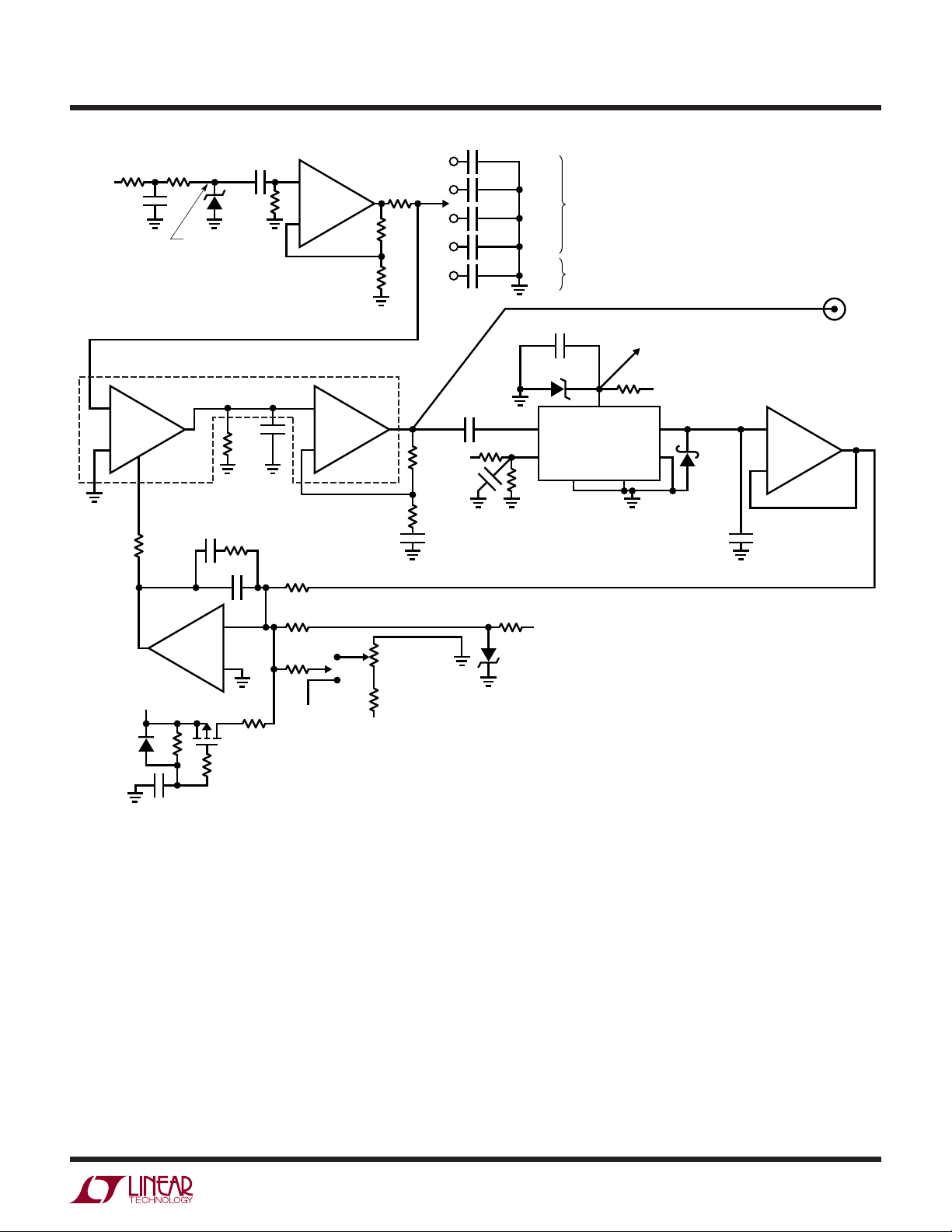
RMS Leveled Output Random Noise Generator
Figure 17 uses the RMS-to-DC converter in a leveled
output random noise generator. Noise diode D1 AC biases
6
A1, operating at a gain of 2.
A1’s output feeds a 1kHz to
500kHz switch selectable lowpass fi lter. The fi lter output
biases the variable gain amplifi er, A2-A3. A2-A3, contained
6
See Appendix C “Symmetrical White Gaussian Noise,” guest written by
Ben Hessen-Schmidt of Noise Com, Inc. for turorial on noise and noise
diodes.
AN106-10
an106f
Application Note 106
15V
NOISE DIODE NOISE DIODE
75k
75k
1µF
7VDC TO 10VDC
+NOISE
VARIABLE GAIN AMPLIFIER
+
A2
I
SET
–
GAIN CONTROL AMPLIFIER
3k
A5
1/2 LT1013
1µF
–
+
LT1228
100pF
900Ω
150k
0.1µF
10µF
1kNC103
475k*
1.1M*
909k*
+
A1
LT1220
–
+
–
INTERNAL
PREAMP
A3
160Ω
1k
1k
AMPLITUDE
10k
ADJUST
510Ω
5Ω
10µF
0.01µF
+V
Z
0.1µF
1µF
0.1µF
0.01µF
0.002µF
500pF
10k
4.7k
FILTER
1kHz
10kHz
100kHz
500kHz
500kHz
1µF
1N4689 5.1V
IN1 OUT
IN2
10k
–15V
LT1004-1.2V
–3dB
FLAT
TO ALL +V
Z
POINTS
1.5k
15V
+V
RMS CONVERTER
+
LTC1968
OUT RTN
EN GND
*1% METAL FILM RESISTOR
CONNECTIONS INSIDE DASHED LINES WITHIN A SINGLE IC
NC103 = NOISE COM
10µF = WIMA MKS-2
1N5712
1/2 LT1013
–
1µF
RMS
AMPLITUDE
STABILIZED
NOISE OUTPUT
A4
AN106 F17
15V
1M1N4148
0.33µF
Q1
TPO610L
1M
510k
SOFT-START
EXTERNAL
0V TO 1V
+V
40.2k*
Z
Figure 17. An RMS Levelled Output Random Noise Generator. Amplifi ed (A1) Diode Noise Is Filtered, Variable Gain Amplifi ed (A2-A3)
and RMS Converted. Converter Output Feeds Back to A5 Gain Control Amplifi er, Closing RMS Stabilized Loop. Output Amplitude, Taken
at A3, is Settable
on one chip, include a current controlled transconductance
amplifi er (A2) and an output amplifi er (A3). This stage takes
AC gain, biases the LTC1968 RMS-to-DC converter and
is the circuit’s output. The RMS converter output at A4,
feeds back to gain control amplifi er A5, which compares
the RMS value to a variable portion of the 5.1V zener
potential. A5’s output sets A2’s gain via the 3k resistor,
completing a control loop to stabilize noise RMS output
stabilize this loop. Output amplitude is variable by the 10k
potentiometer; a switch permits external voltage control.
Q1 and associated components, a soft-start circuit, prevent
output overshoot at power turn-on.
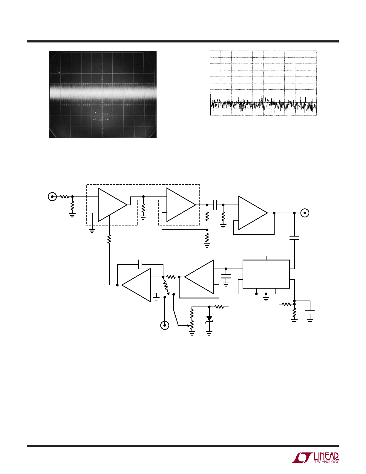
Figure 18 shows circuit output noise in the 10kHz fi lter
position; Figure 19’s spectral plot reveals essentially fl at
RMS noise amplitude over a 500kHz bandwidth.
amplitude. The RC components in A5’s local feedback path
an106f
AN106-11
Application Note 106
2V/DIV
5ms/DIV
AN106 F18
Figure 18. Figure 17’s Output in the 10kHz Filter Position
0.4V
INPUT
RMS
5V
RMS
TO
10k
100Ω
VARIABLE GAIN AMPLIFIER
+
A1
1/2 LT1228
300Ω
–
1k
0.15µF
–
A5
1/2 LT1013
+
GAIN CONTROL
AMPLIFIER
EXT INPUT
0V TO –0.5V
TO 0.5V
0V
RMS
OUTPUT
+
A2
1/2 LT1228
–
100k*
100k*
RMS
–3dB/DIV
AMPLITUDE VARIANCE
0 50 100 150 200 250
FREQUENCY (kHz)
300 350 400 450 500
AN106 F19
Figure 19. Amplitude vs Frequency for the Random Noise
Generator is Essentially Flat to 500kHz. NC103 Diode Contributes
Even Noise Spectrum Distribution; RMS Converter and Loop
Stabilize Amplitude. Sweep Time is 2.8 Minutes, Resolution
Bandwidth, 100Hz
1µF
470Ω
10k
OUTPUT BUFFER
+
A3
LT1220
RMS LEVELLED
OUTPUT
TO 0.5V
0V
RMS
RMS
–
0V
RMS
A4
1/2 LT1013
13.3k*
10k
OUTPUT
LEVEL
TO 0.5V
10Ω
RMS CONVERTER
+
–
4.7k
–5V
LT1004
1.2V
REFERENCE
RMS
5V
+
OUT IN1
1µF
OUT RTN IN2
*0.1% METAL FILM RESISTOR
CONNECTIONS INSIDE DASHED
LINES ARE WITHIN A SINGLE IC
V
C1
LTC1968
GND EN
5V
1µF
10k
10k 0.1µF
AN106 F20
Figure 20. RMS Amplitude Level Control Uses Figure 17’s Gain Control Loop. A1-A3 Provide Variable Gain to Input. RMS Converter
Feeds Back to A5 Gain Control Amplifi er, Closing Amplitude Stabilization Loop. Variable Reference Permits Settable, Calibrated RMS
Output Amplitude Independent of Input Waveshape
RMS Amplitude Stabilized Level Controller
Figure 20 borrows the previous circuit’s gain control
loop to stabilize the RMS amplitude of an arbitrary input
waveform. The unregulated input is applied to variable gain
amplifi er A1-A2 which feeds A3. DC coupling at A1-A2
permits passage of low frequency inputs. A3’s output is
taken by RMS-to-DC converter C1-A4, which feeds the
A5 gain control amplifi er. A5 compares the RMS value to
a variable reference and biases A1, closing a gain control
loop. The 0.15µF feedback capacitor stabilizes this loop,
even for waveforms below 100Hz. This feedback action
stabilizes output RMS amplitude despite large variations
an106f
AN106-12
Application Note 106
in input amplitude while maintaining waveshape. Desired
output level is settable with the indicated potentiometer or
an external control voltage may be switched in.
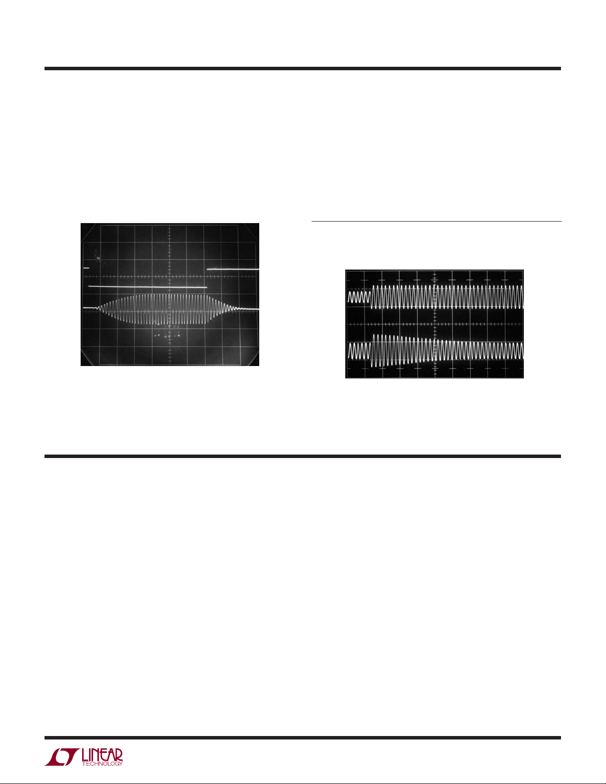
Figure 21 shows output response (trace B) to abrupt reference level set point changes (trace A). The output settles
within 60 milliseconds for ascending and descending
transitions. Faster response is possible by decreasing A5’s
compensation capacitor, but low frequency waveforms
A = 0.5V/DIV
B = 1V/DIV
20ms/DIV
Figure 21. Amplitude Level Control Response (Trace B) to
Abrupt Reference Changes (Trace A). Settling Time is Set by
A5’s Compensation Capacitor, Which Must be Large Enough
to Stabilize Loop at Lowest Expected Input Frequency
AN106 F21
would not be processable. Similar considerations apply to
Figure 22’s response to an input waveform step change.
Trace A is the circuit’s input and trace B its output. The
output settles in 60 milliseconds due to A5’s compensation. Reducing compensation value speeds response at the
expense of low frequency waveform processing capability.
Specifi cations include 0.1% output amplitude stability
for inputs varying from 0.4V
RMS
to 5V
, 1% set point
RMS
accuracy, 0.1kHz to 500kHz passband and 0.1% stability
for 20% power supply deviation.
Note: This Application Note was derived from a manuscript originally
prepared for publication In EDN magazine.
A = 2V/DIV
B = 1V/DIV
10ms/DIV
Figure 22. Amplitude Level Control Output Reacts (Trace B) to
Input Step Change (Trace A). Slow Loop Compensation Allows
Overshoot But Output Settles Cleanly
AN106 F22
REFERENCES
1. Hewlett-Packard Company, “1968 Instrumentation.
Electronic—Analytical—Medical,” AC Voltage Measurement, Hewlett-Packard Company, 1968, pp. 197-198.
2. Sheingold, D. H. (editor), “Nonlinear Circuits Handbook,” 2nd Edition, Analog Devices, Inc., 1976.
3. Lambda Electronics, Model LK-343A-FM Manual.
4. Grafham, D. R., “Using Low Current SCRs,” General
Electric AN200.19. Jan. 1967.
5. Williams, J., “Performance Enhancement Techniques
for Three-Terminal Regulators,” Linear Technology Corp.
AN-2. August, 1984. “SCR Preregulator,” pp. 3-6.
6. Williams, J., “High Effi ciency Linear Regulators,”
Linear Technology Corporation, Application Note 32, “SCR
Preregulator.” March 1989, pp. 3-4.
7. Williams, J., “High Speed Amplifi er Techniques,” Linear
Technology Corporation, Application Note 47, “Parallel
Path Amplifi ers,” August 1991, pp. 35-37.
8. Williams, J., “Practical Circuitry for Measurement and
Control Problems,” Broadband Random Noise Generator,”
“Symmetrical White Gaussian Noise,” Appendix B, Linear
Technology Corporation, Application Note 61, August 1994,
pp.24-26, pp. 38-39.
9. Williams, J., “A Fourth Generation of LCD Backlight
Technology,” “RMS Voltmeters,” Linear Technology Corporation, Application Note 65, November 1995, pp. 82-83.
10. Meacham, L. A., “The Bridge Stabilized Oscillator,”
Bell System Technical Journal, Vol. 17, p. 574, October
1938.
11. Williams, Jim, “Bridge Circuits—Marrying Gain and
Balance,” Linear Technology Corporation, Application Note
43, June, 1990.
an106f
AN106-13

Application Note 106
APPENDIX A
RMS-TO-DC CONVERSION
Joseph Petrofsky
Defi nition of RMS
RMS amplitude is the consistent, fair and standard way to
measure and compare dynamic signals of all shapes and
sizes. Simply stated, the RMS amplitude is the heating
potential of a dynamic waveform. A 1V
AC waveform
RMS
will generate the same heat in a resistive load as will 1V
DC. See Figure A1.
Mathematically, RMS is the “Root of the Mean of the
Square”:
VV
RMS
2
=
+
R1V DC
–
1V AC
RMS
R
R1V (AC + DC) RMS
SAME
HEAT
AN106 FA1
The last two entries of Table A1 are chopped sine waves
as is commonly created with thyristors such as SCRs and
Triacs. Figure A2a shows a typical circuit and Figure A2b
shows the resulting load voltage, switch voltage and load
currents. The power delivered to the load depends on the
fi ring angle, as well as any parasitic losses such as switch
“ON” voltage drop. Real circuit waveforms will also typically have signifi cant ringing at the switching transition,
dependent on exact circuit parasitics. Here, “SCR Waveforms” refers to the ideal chopped sine wave, though the
LTC1966/LTC1967/LTC1968 will do faithful RMS-to-DC
conversion with real SCR waveforms as well.
The case shown is for Θ = 90°, which corresponds to 50%
of available power being delivered to the load. As noted
in Table A1, when Θ = 114°, only 25% of the available
power is being delivered to the load and the power drops
quickly as Θ approaches 180°.
With an average rectifi cation scheme and the typical
calibration to compensate for errors with sine waves, the
RMS level of an input sine wave is properly reported; it is
only with a non-sinusoidal waveform that errors occur.
Because of this calibration, and the output reading in V
RMS
,
the term True-RMS got coined to denote the use of an
actual RMS-to-DC converter as opposed to a calibrated
average rectifi er.
Figure A1
Alternatives to RMS
Other ways to quantify dynamic waveforms include peak
detection and average rectifi cation. In both cases, an average (DC) value results, but the value is only accurate at
the one chosen waveform type for which it is calibrated,
typically sine waves. The errors with average rectifi cation
are shown in Table A1. Peak detection is worse in all cases
and is rarely used.
Table A1. Errors with Average Rectifi cation vs True RMS
AVERAGE
RECTIFIED
WAVEFORM V
Square Wave 1.000 1.000 11%
Sine Wave 1.000 0.900 *Calibrate for 0% Error
Triangle Wave 1.000 0.866 –3.8%
SCR at 1/2 Power,
Θ = 90°
SCR at 1/4 Power,
Θ = 114°
RMS
1.000 0.637 –29.3%
1.000 0.536 –40.4%
(V) ERROR*
MAINS
V
LOAD
+
–
I
LOAD
+
AC
V
LINE
CONTROL
–
+
V
–
AN106 FA2a
THY
Figure A2a
V
LINE
Θ
V
LOAD
V
THY
I
LOAD
AN106 FA2b
Figure A2b
an106f
AN106-14

Application Note 106
How an RMS-to-DC Converter Works
Monolithic RMS-to-DC converters use an implicit computation to calculate the RMS value of an input signal. The
fundamental building block is an analog multiply/divide
used as shown in Figure A3. Analysis of this topology is
easy and starts by identifying the inputs and the output
of the lowpass fi lter. The input to the LPF is the calculation from the multiplier/divider; (V
IN
)2/V
. The lowpass
OUT
fi lter will take the average of this to create the output,
mathematically:
2
⎛
V
=
⎜
OUT
⎜
⎝
Because V is DC,
2
⎛
⎜
⎜
⎝
⎞
VV
()
IN
⎟
V
⎟
OUT
⎠
()
V
=
OUT
2
VVor
()
VV
OUT IN
Figure A3 RMS-to-DC Converter with Implicit Computation
=
OUT IN
=
V
⎞
V
()
IN
,
⎟
V
⎟
OUT
⎠
OUT
2
V
()
IN
()
so
V
OUT
2
,
2
2
,
and
,
=
RRMS V
()
IN
()
V
÷×
V
OUT
IN
LPF
2
AN106 FA3
=
V
(()
IN
V
OUT
()
()
IN
V
OUT
Unlike the prior generation RMS-to-DC converters, the
LTC1966/LTC1967/LTC1968 computation does NOT use
log/antilog circuits, which have all the same problems,
and more, of log/antilog multipliers/dividers, i.e., linearity
is poor, the bandwidth changes with the signal amplitude
and the gain drifts with temperature.
How the LTC1966/LTC1967/LTC1968 RMS-to-DC
Converters Work
The LTC1966/LTC1967/LTC1968 use a completely new
topology for RMS-to-DC conversion, in which a ΔΣ modulator acts as the divider, and a simple polarity switch is
used as the multiplier as shown in Figure A4.
V
IN
D
α
V
OUT
∆-Σ
REF
V
IN
±1
LPF
AN106 FA4
Figure A4. Topology of the LTC1966/LTC1967/LTC1968
V
OUT
The ΔΣ modulator has a single-bit output whose average
⎯
duty cycle (
D) will be proportional to the ratio of the input
signal divided by the output. The ΔΣ is a 2nd order modulator with excellent linearity. The single-bit output is used to
selectively buffer or invert the input signal. Again, this is a
circuit with excellent linearity, because it operates at only
two points: ±1 gain; the average effective multiplication over
time will be on the straight line between these two points.
The combination of these two elements again creates a
lowpass fi lter input signal equal to (V
IN
)2/V
, which, as
OUT
shown above, results in RMS-to-DC conversion.
The lowpass fi lter performs the averaging of the RMS func-
tion and must be a lower corner frequency than the lowest
frequency of interest. For line frequency measurements,
this fi lter is simply too large to implement on-chip, but
the LTC1966/LTC1967/LTC1968 need only one capacitor
on the output to implement the lowpass fi lter. The user
can select this capacitor depending on frequency range
and settling time requirements.
This topology is inherently more stable and linear than
log/antilog implementations primarily because all of the
signal processing occurs in circuits with high gain op
amps operating closed loop.
Note that the internal scalings are such that the ΔΣ output duty cycle is limited to 0% or 100% only when V
exceeds ±4 • V
OUT
.
IN
an106f
AN106-15
Application Note 106
Linearity of an RMS-to-DC Converter
Linearity may seem like an odd property for a device that
implements a function that includes two very nonlinear
processes: squaring and square rooting.
However, an RMS-to-DC converter has a transfer function,
RMS volts in to DC volts out, that should ideally have a
1:1 transfer function. To the extent that the input to output
transfer function does not lie on a straight line, the part
is nonlinear.
A more complete look at linearity uses the simple model
shown in Figure A5. Here an ideal RMS core is corrupted by
both input circuitry and output circuitry that have imperfect
transfer functions. As noted, input offset is introduced in
the input circuitry, while output offset is introduced in the
output circuitry.
Any nonlinearity that occurs in the output circuity will corrupt the RMS in to DC out transfer function. A nonlinearity
in the input circuitry will typically corrupt that transfer
function far less simply because with an AC input, the
RMS-to-DC conversion will average the nonlinearity from
a whole range of input values together.
But the input nonlinearity will still cause problems in
an RMS-to-DC converter because it will corrupt the accuracy as the input signal shape changes. Although an
RMS-to-DC converter will convert any input waveform to
a DC output, the accuracy is not necessarily as good for
all waveforms as it is with sine waves. A common way
to describe dynamic signal wave shapes is Crest Factor.
The crest factor is the ratio of the peak value relative to
the RMS value of a waveform. A signal with a crest factor
of 4, for instance, has a peak that is four times its RMS
value. Because this peak has energy (proportional to volt-
2
age squared) that is 16 times (4
) the energy of the RMS
value, the peak is necessarily present for at most 6.25%
(1/16) of the time.
The LTC1966/LTC1967/LTC1968 perform very well with
crest factors of 4 or less and will respond with reduced
accuracy to signals with higher crest factors. The high
performance with crest factors less than 4 is directly
attributable to the high linearity throughout the LTC1966/
LTC1967/LTC1968.
INPUT CIRCUITRY
INPUT OUTPUT
• V
IOS
• INPUT NONLINEARITY
Figure A5. Linearity Model of an RMS-to-DC Converter
IDEAL
RMS-TO-DC
CONVERTER
OUTPUT CIRCUITRY
• V
OOS
• OUTPUT NONLINEARITY
AN106 FA5
an106f
AN106-16

Application Note 106
APPENDIX B
AC Measurement and Signal Handling Practice
Accurate AC measurement requires trustworthy instrumentation, proper signal routing technique, parasitic
minimization, attention to layout and care in component
selection. The text circuits DC-500kHz, 1% error bandwidth seems benign, but unpleasant surprises await the
unwary.
An accurate RMS voltmeter is required for serious AC
work. Figure B1 lists types used in our laboratory. These
are high grade, specialized instruments specifi cally intended for precise RMS measurement. All are thermally
1
based
. The fi rst three entries, general purpose instruments with many ranges and features, are easily used and
meet almost all AC measurement needs. The last entry is
more of a component than an instrument. The A55 series
of “thermal converters” provide millivolt level outputs
for various inputs. Typical input ranges are 0.5V
1V
RMS
, 2V
RMS
and 5V
and each converter is sup-
RMS
RMS
,
plied with individual calibration data. They are somewhat
cumbersome to use and easily destroyed but are highly
accurate. Their primary use is as reference standards to
check other instrument’s performance.
AC signal handling for high accuracy is a broad topic,
involving a considerable degree of depth. This forum
must suffer brevity, but some gossip is possible.
Layout is critical. The most prevalent parasitic in AC
measurement is stray capacitance. Keep signal path
connections short and small area. A few picofarrads of
coupling into a high impedance node can upset a 500kHz,
1% accuracy signal path. To the extent possible, keep
impedances low to minimize parasitic capacitive effects.
Consider individual component parasitics and plan to
accommodate them. Examine effects of component
placement and orientation on the circuit board. If a
ground plane is in use it may be necessary to relieve it
in the vicinity of critical circuit nodes or even individual
components.
Passive components have parasitics that must be kept in
mind. Resistors suffer shunt capacitance whose effects
vary with frequency and resistor value. It is worth noting
that different brands of resistors, although nominally
similar, may exhibit markedly different parasitic behavior. Capacitors in the signal path should be used so that
their outer foil is connected to the less sensitive node,
affording some relief from pick-up and stray capacitance
induced effects. Some capacitors are marked to indicate
the outer foil terminal, others require consulting the
data sheet or vendor contact. Avoid ceramic capacitors
in the signal path. Their piezoelectric responses make
them unsuitable for precision AC circuitry. In general,
any component in the signal path should be examined
in terms of its potential parasitic contribution.
1
See references 1 and 2 for details on thermally based RMS-to-DC
conversion.
MODEL MANUFACTURER 1V RANGE INPUT BANDWIDTH COMMENTS
3400A/3400B Hewlett-Packard 1% AC 10MHz/20MHz Metered Instrument. Most Common RMS
3403C Hewlett-Packard 0.2% AC, AC + DC 100MHz Digital Display, 1µV Sensitivity (2MHz BW),
8920/8921A Fluke 0.7% AC, AC + DC 20MHz Digital Display, 10µV Sensitivity (2MHz BW),
A55 Fluke 0.05% AC + DC 50MHz Set of Individually Calibrated Thermal
Figure B1. Precision Wideband RMS Voltmeters Useful for AC Measurement. All are Thermally Based, Permitting High Accuracy
and Wide Bandwidth Independent of Input Waveshape. A55 Reference Standards, Although Unsuitable for General Purpose
Measurement, Have Best Accuracy
Voltmeter
dB Ranges, Relative dB
dB Ranges, Relative dB
Converters. Reference Standards. Not for
General Purpose Measurement
an106f
AN106-17

Application Note 106
Active components, such as amplifi ers, must be treated
as potential error sources. In particular, as stated in the
text, ensure that there is enough open loop gain at the
frequency of interest to assure needed closed loop gain
accuracy. Margins of 100:1 are not unreasonable. Keep
feedback values as low as possible to minimize parasitic
effects.
Route signals to and from the circuit board coaxially and
at low impedance, preferably 50Ω, for best results. In
50Ω systems, remember that terminators and attenuators
APPENDIX C
Symmetrical White Gaussian Noise
by Ben Hessen-Schmidt,
NOISE COM, INC.
White noise provides instantaneous coverage of all frequencies within a band of interest with a very fl at output
spectrum. This makes it useful both as a broadband
stimulus and as a power-level reference.
Symmetrical white Gaussian noise is naturally generated in
resistors. The noise in resistors is due to vibrations of the
conducting electrons and holes, as described by Johnson
and Nyquist.
metrically Gaussian, and the average noise voltage is:
VkT
n
where:
k = 1.38E–23 J/K (Boltzmann’s constant)
T = temperature of the resistor in Kelvin
f = frequency in Hz
h = 6.62E–34 Js (Planck’s constant)
R(f) = resistance in ohms as a function of frequency
1
The distribution of the noise voltage is sym-
=∫2 R(f) p(f) df
(1)
have tolerances that can corrupt a 1% amplitude accuracy
measurement. Verify such terminator and attenuator
tolerances by measurement and account for them when
interpreting measurement results. Similarly, verify the
accuracy of any associated instruments 50Ω input or
output impedance and account for deviations.
This all seems painful but is an essential part of achieving
1% accurate, 500kHz signal integrity. Failure to observe
the precautions listed above risks degrading the RMSto-DC converters system level performance.
p(f) is close to unity for frequencies below 40GHz when T
is equal to 290°K. The resistance is often assumed to be
independent of frequency, and Údf is equal to the noise
bandwidth (B). The available noise power is obtained when
the load is a conjugate match to the resistor, and it is:
2
V
n
N
==
where the “4” results from the fact that only half of the
noise voltage and hence only 1/4 of the noise power is
delivered to a matched load.
Equation 3 shows that the available noise power is proportional to the temperature of the resistor; thus it is often
called thermal noise power, Equation 3 also shows that
white noise power is proportional to the bandwidth.
An important source of symmetrical white Gaussian noise
is the noise diode. A good noise diode generates a high
level of symmetrical white Gaussian noise. The level is
often specifi ed in terms of excess noise ratio (ENR).
ENR in Log
kTB
R
4
dB
()
Te
−
=
10
()
290
290
(3)
(4)
pf
()=
exp(hf/kT) 1
kT
[]
AN106-18
hf
(2)
−
Te is the physical temperature that a load (with the same
impedance as the noise diode) must be at to generate the
same amount of noise.
1
See “Additional Reading” at the end of this section.
an106f

Application Note 106
The ENR expresses how many times the effective noise
power delivered to a non-emitting, nonrefl ecting load
exceeds the noise power available from a load held at the
reference temperature of 290°K (16.8°C or 62.3°F).
The importance of high ENR becomes obvious when the
noise is amplifi ed, because the noise contributions of the
amplifi er may be disregarded when the ENR is 17dB larger
than the noise fi gure of the amplifi er (the difference in
total noise power is then less than 0.1dB). The ENR can
easily be converted to noise spectral density in dBm/Hz
or µV/√Hz by use of the white noise conversion formulas
in Table 1.
Table 1. Useful White Noise Conversion
dBm
dBm
dBm
dBm/Hz
dBm/Hz
=
dBm/Hz + 10log (BW)
=
20log (Vn) – 10log(R) + 30dB
=
20log(Vn) + 13dB for R = 50Ω
=
20log(µVn√
=
–174dBm/Hz + ENR for ENR > 17dB
Hz
) – 10log(R) – 90dB
When amplifying noise it is important to remember that
the noise voltage has a Gaussian distribution. The peak
voltages of noise are therefore much larger than the average
or RMS voltage. The ratio of peak voltage to RMS voltage
is called crest factor, and a good crest factor for Gaussian
noise is between 5:1 and 10:1 (14 to 20dB). An amplifi er’s
1dB gain-compression point should therefore be typically
20dB larger than the desired average noise-output power
to avoid clipping of the noise.
For more information about noise diodes, please contact
NOISE COM, INC. at (973) 386-9696.
Additional Reading
1. Johnson, J.B, “Thermal Agitation of Electricity in Conductors,” Physical Review, July 1928, pp. 97-109.
2. Nyquist, H. “Thermal Agitation of Electric Charge in Conductors,” Physical Review, July 1928, pp. 110-113.
Information furnished by Linear Technology Corporation is believed to be accurate and reliable.
However, no responsibility is assumed for its use. Linear Technology Corporation makes no representation that the interconnection of its circuits as described herein will not infringe on existing patent rights.
an106f
AN106-19

Application Note 106
AN106-20
Linear Technology Corporation
1630 McCarthy Blvd., Milpitas, CA 95035-7417
(408) 432-1900 ● FAX: (408) 434-0507
●
www.linear.com
an106f
LT 0207 • PRINTED IN USA
© LINEAR TECHNOLOGY CORPORATION 2007
 Loading...