

FEATURES
■
High Efficiency: Over 90%
■
High Output Currents Easily Achieved
■
Wide VIN Range: 2.5V to 9.8V
■
V
Limited Only by External Components
OUT
■
Constant Frequency 550kHz Operation
■
Burst Mode
■
Current Mode Operation for Excellent Line and Load
TM
Operation at Light Load
Transient Response
■
Low Quiescent Current: 270µA
■
Shutdown Mode Draws Only 8µA Supply Current
■
±2.5% Reference Accuracy
■
Tiny 6-Lead SOT-23 Package
U
APPLICATIO S
■
Lithium-Ion-Powered Applications
■
Cellular Telephones
■
Wireless Modems
■
Portable Computers
■
Scanners
LTC1872
Constant Frequency
Current Mode Step-Up
DC/DC Controller in SOT-23
U
DESCRIPTIO
The LTC®1872 is a constant frequency current mode stepup DC/DC controller providing excellent AC and DC load
and line regulation. The device incorporates an accurate
undervoltage lockout feature that shuts down the LTC1872
when the input voltage falls below 2.0V.
The LTC1872 boasts a ±2.5% output voltage accuracy and
consumes only 270µA of quiescent current. For applica-
tions where efficiency is a prime consideration, the LTC1872
is configured for Burst Mode operation, which enhances
efficiency at low output current.
In shutdown, the device draws a mere 8µA. The high
550kHz constant operating frequency allows the use of a
small external inductor.
The LTC1872 is available in a small footprint 6-lead
SOT-23.
, LTC and LT are registered trademarks of Linear Technology Corporation.
Burst Mode is a trademark of Linear Technology Corporation.
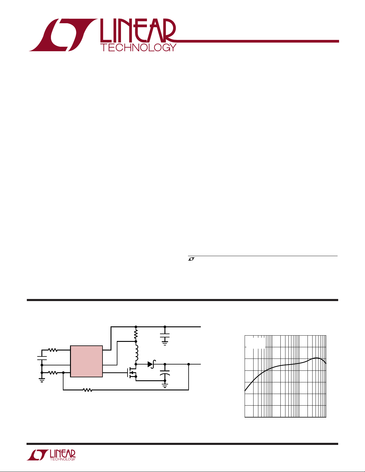
TYPICAL APPLICATION
147k
220pF
80.6k
C1: TAIYO YUDEN CERAMIC EMK325BJ106MNT
C2: MURATA GRM42-2X5R226K6.3
D1: IR10BQ015
L1: MURATA LQN6C4R7M04
M1: IRLMS2002
R1: DALE 0.25W
1
2
3
ITH/RUN
LTC1872
GND
V
FB
422k
Figure 1. LTC1872 High Output Current 3.3V to 5V Boost Converter
SENSE
NGATE
5
V
IN
4
–
6
U
R1
0.03Ω
L1
4.7µH
M1
V
IN
C1
10µF
10V
+
D1
C2
2× 22µF
6.3V
3.3V
V
5V
1A
1872 TA01
OUT
EFFICIENCY (%)
Efficiency vs Load Current
100
VIN = 3.3V
= 5V
V
OUT
95
90
85
80
75
70
65
1
10 100 1000
LOAD CURRENT (mA)
1872 TA01b
1
LTC1872
ITH/RUN 1
GND 2
V
FB
3
6 NGATE
5 V
IN
4 SENSE
–
TOP VIEW
S6 PACKAGE
6-LEAD PLASTIC SOT-23
WW
W
ABSOLUTE MAXIMUM RATINGS
U
U
W
PACKAGE/ORDER INFORMATION
(Note 1)
Input Supply Voltage (VIN).........................–0.3V to 10V
SENSE–, NGATE Voltages ............ – 0.3V to (VIN + 0.3V)
VFB, ITH/RUN Voltages ..............................–0.3V to 2.4V
NGATE Peak Output Current (<10µs) ....................... 1A
ORDER PART
NUMBER
LTC1872ES6
Storage Ambient Temperature Range ... –65°C to 150°C
Operating Temperature Range (Note 2) .. –40°C to 85°C
S6 PART MARKING
Junction Temperature (Note 3)............................. 150°C
Lead Temperature (Soldering, 10 sec).................. 300°C
Consult factory for parts specified with wider operating temperature ranges.
ELECTRICAL CHARACTERISTICS
range, otherwise specifications are at TA = 25°C. VIN = 4.2V unless otherwise specified. (Note 2)
PARAMETER CONDITIONS MIN TYP MAX UNITS
Input DC Supply Current Typicals at VIN = 4.2V (Note 4)
Normal Operation 2.4V ≤ V
Sleep Mode 2.4V ≤ V
Shutdown 2.4V ≤ V
UVLO V
Undervoltage Lockout Threshold VIN Falling ● 1.55 2.00 2.35 V
V
IN
Shutdown Threshold (at ITH/RUN) ● 0.15 0.35 0.55 V
Start-Up Current Source V
Regulated Feedback Voltage 0°C to 70°C(Note 5) ● 0.780 0.800 0.820 V
VFB Input Current (Note 5) 10 50 nA
Oscillator Frequency VFB = 0.8V 500 550 650 kHz
Gate Drive Rise Time C
Gate Drive Fall Time C
Peak Current Sense Voltage (Note 6) 114 120 mV
ITH
–40°C to 85°C(Note 5)
LOAD
LOAD
The ● denotes specifications that apply over the full operating temperature
≤ 9.8V 270 420 µA
IN
≤ 9.8V 230 370 µA
IN
≤ 9.8V, V
IN
< UVLO Threshold 6 10 µA
IN
Rising 1.85 2.10 2.40 V
/RUN = 0V 0.25 0.5 0.85 µA
= 3000pF 40 ns
= 3000pF 40 ns
ITH
T
= 150°C, θJA = 230°C/W
JMAX
/RUN = 0V 8 22 µA
● 0.770 0.800 0.830 V
LTMK
U
Note 1: Absolute Maximum Ratings are those values beyond which the life
of a device may be impaired.
Note 2: The LTC1872E is guaranteed to meet performance specifications
from 0°C to 70°C. Specifications over the –40°C to 85°C operating
temperature range are assured by design, characterization and correlation
with statistical process controls.
Note 3: T
dissipation P
is calculated from the ambient temperature TA and power
J
according to the following formula:
D
TJ = TA + (PD • θJA°C/W)
2
Note 4: Dynamic supply current is higher due to the gate charge being
delivered at the switching frequency.
Note 5: The LTC1872 is tested in a feedback loop that servos V
output of the error amplifier.
Note 6: Guaranteed by design at duty cycle = 30%. Peak current sense
voltage is V
increases due to slope compensation as shown in Figure 2.
/6.67 at duty cycle <40%, and decreases as duty cycle
REF
to the
FB
W
U
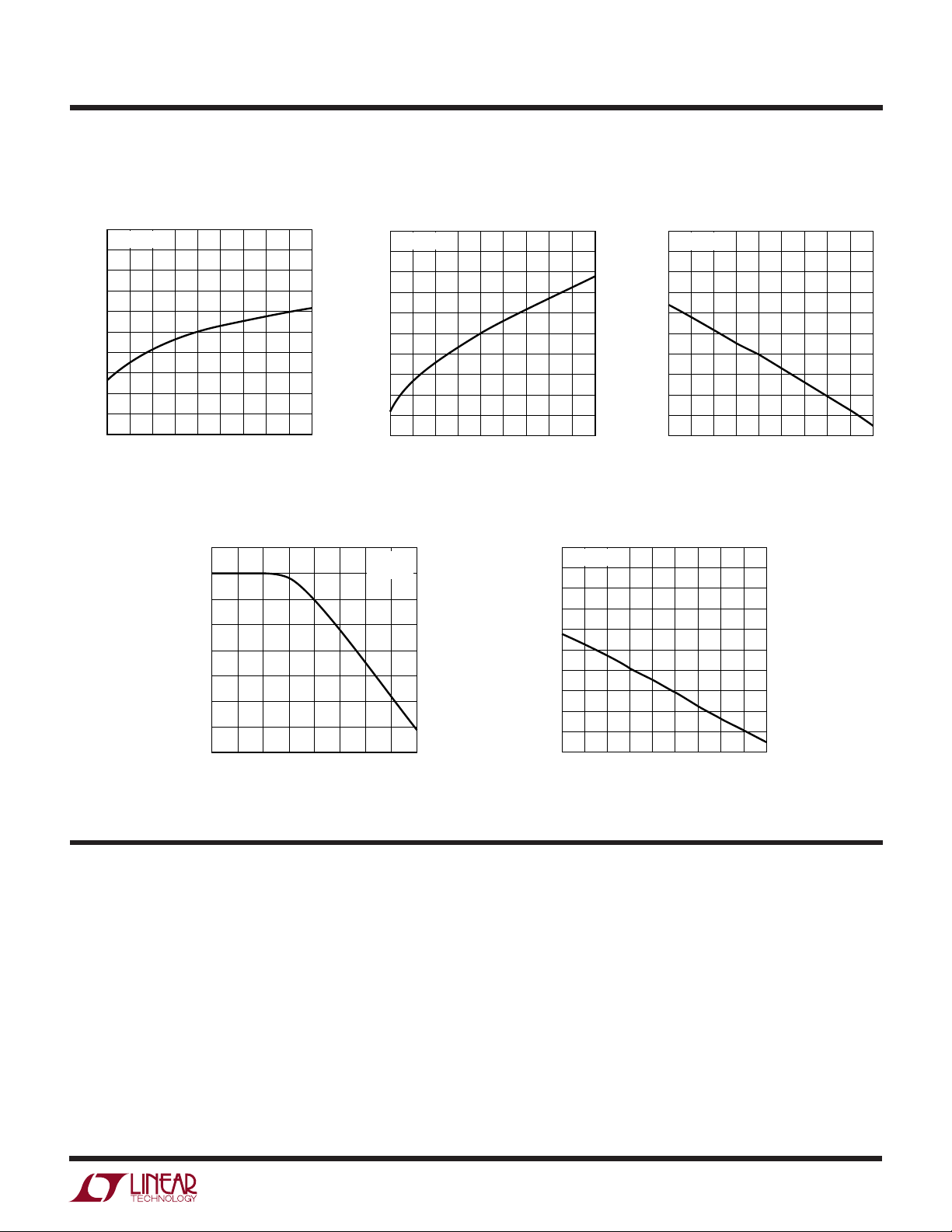
TYPICAL PERFORMANCE CHARACTERISTICS
LTC1872
Reference Voltage
vs Temperature
825
VIN = 4.2V
820
815
810
805
800
795
VOLTAGE (mV)
FB
V
790
785
780
775
–35 5
–15
–55
85
45 125
25
TEMPERATURE (°C)
105
65
1872 G01
Maximum Current Sense Trip
Voltage vs Duty Cycle
130
120
110
100
– (mV)
90
SENSE
– V
80
IN
V
70
60
50
20 30
40 50
DUTY CYCLE (%)
60 70
Normalized Oscillator Frequency
vs Temperature
10
VIN = 4.2V
8
6
4
2
0
–2
–4
–6
NORMALIZED FREQUENCY (%)
–8
–10
–35 5
–55
VIN = 4.2V
T
= 25°C
A
80 90
–15
TEMPERATURE (°C)
100
1872 G04
45 125
65
25
85
105
1872 G02
Shutdown Threshold
vs Temperature
600
VIN = 4.2V
560
520
480
440
400
360
/RUN VOLTAGE (mV)
320
TH
I
280
240
200
–35 5
–15
–55
TEMPERATURE (
Undervoltage Lockout Trip
Voltage vs Temperature
2.24
VIN FALLING
2.20
2.16
2.12
2.08
2.04
2.00
1.96
UVLO TRIP VOLTAGE (V)
1.92
1.88
1.84
–35 5
–15
–55
45 125
65
25
°C)
25
TEMPERATURE (°C)
85
105
1872 G05
85
45 125
105
65
1872 G03
UUU
PIN FUNCTIONS
ITH/RUN (Pin 1): This pin performs two functions. It
serves as the error amplifier compensation point as well as
the run control input. Nominal voltage range for this pin is
0.7V to 1.9V. Forcing this pin below 0.35V causes the
device to be shut down. In shutdown all functions are
disabled and the NGATE pin is held low.
GND (Pin 2): Ground Pin.
VFB (Pin 3): Receives the feedback voltage from an exter-
nal resistive divider across the output.
SENSE– (Pin 4): The Negative Input to the Current Comparator.
VIN (Pin 5): Supply Pin. Must be closely decoupled to GND
Pin 2.
NGATE (Pin 6): Gate Drive for the External N-Channel
MOSFET. This pin swings from 0V to VIN.
3
LTC1872
UU
W
FUNCTIONAL DIAGRA
–
SENSE
V
IN
5
4
4
+
ICMP
–
OSC
FREQ
FOLDBACK
V
IN
+
0.3V
GND
2
–
SLOPE
COMP
–
+
0.5µA
V
IN
VOLTAGE
REFERENCE
UNDERVOLTAGE
LOCKOUT
0.3V
0.15V
V
REF
0.8V
0.35V
V
RS
R
Q
S
+
–
I
/RUN
1
TH
+
–
BURST
CMP
SHDN
CMP
SWITCHING
LOGIC AND
BLANKING
CIRCUIT
SLEEP
SHDN
UV
OVP
EAMP
IN
NGATE
6
+
V
REF
+
–
60mV
V
REF
+
0.8V
–
1.2V
V
FB
3
V
IN
1872FD
U
OPERATIO
Main Control Loop
The LTC1872 is a constant frequency current mode switching regulator. During normal operation, the external
N-channel power MOSFET is turned on each cycle by the
oscillator and turned off when the current comparator
(ICMP) resets the RS latch. The peak inductor current at
which ICMP resets the RS latch is controlled by the voltage
on the ITH/RUN pin, which is the output of the error
amplifier EAMP. An external resistive divider connected
between V
output feedback voltage VFB. When the load current increases, it causes a slight decrease in VFB relative to the
and ground allows the EAMP to receive an
OUT
(Refer to Functional Diagram)
4
0.8V reference, which in turn causes the
ITH/RUN voltage to increase until the average inductor
current matches the new load current.
The main control loop is shut down by pulling the ITH/RUN
pin low. Releasing ITH/RUN allows an internal 0.5µA
current source to charge up the external compensation
network. When the ITH/RUN pin reaches 0.35V, the main
control loop is enabled with the ITH/RUN voltage then
pulled up to its zero current level of approximately 0.7V.
As the external compensation network continues to charge
up, the corre
sponding output current trip level follows,
allowing normal operation.

OPERATIO
LTC1872
U
(Refer to Functional Diagram)
Comparator OVP guards against transient overshoots
>7.5% by turning off the external N-channel power
MOSFET and keeping it off until the fault is removed.
Burst Mode Operation
The LTC1872 enters Burst Mode operation at low load
currents. In this mode, the peak current of the inductor is
set as if V
/RUN = 1V (at low duty cycles) even though
ITH
the voltage at the ITH/RUN pin is at a lower value. If the
inductor’s average current is greater than the load requirement, the voltage at the ITH/RUN pin will drop. When the
ITH/RUN voltage goes below 0.85V, the sleep signal goes
high, turning off the external MOSFET. The sleep signal
goes low when the ITH/RUN voltage goes above 0.925V
and the LTC1872 resumes normal operation. The next
oscillator cycle will turn the external MOSFET on and the
switching cycle repeats.
Undervoltage Lockout
To prevent operation of the N-channel MOSFET below safe
input voltage levels, an undervoltage lockout is incorporated into the LTC1872. When the input supply voltage
drops below approximately 2.0V, the N-channel MOSFET
and all circuitry is turned off except the undervoltage
block, which draws only several microamperes.
Overvoltage Protection
The overvoltage comparator in the LTC1872 will turn the
external MOSFET off when the feedback voltage has risen
7.5% above the reference voltage of 0.8V. This comparator has a typical hysteresis of 20mV.
Slope Compensation and Inductor’s Peak Current
The inductor’s peak current is determined by:
V
−
0710.
I
PK
ITH
=
R
SENSE
()
when the LTC1872 is operating below 40% duty cycle.
However, once the duty cycle exceeds 40%, slope compensation begins and effectively reduces the peak inductor current. The amount of reduction is given by the curves
in Figure 2.
Short-Circuit Protection
Since the power switch in a boost converter is not in series
with the power path from input to load, turning off the
switch provides no protection from a short-circuit at the
output. External means such as a fuse in series with the
boost inductor must be employed to handle this fault
condition.
110
100
90
80
(%)
70
60
OUT(MAX)
/I
50
OUT
SF = I
Figure 2. Maximum Output Current vs Duty Cycle
I
= 0.4I
RIPPLE
AT 5% DUTY CYCLE
40
I
= 0.2I
30
20
10
RIPPLE
AT 5% DUTY CYCLE
VIN = 4.2V
0 70 80 90 1006010 20 30 40 50
DUTY CYCLE (%)
PK
PK
1872 F02
5

LTC1872
U
WUU
APPLICATIONS INFORMATION
The basic LTC1872 application circuit is shown in
Figure␣ 1. External component selection is driven by the
load requirement and begins with the selection of L1 and
R
diode D1 is selected followed by CIN(= C1) and C
R
R
With the current comparator monitoring the voltage developed across R
determines the inductor’s peak current. The output current the LTC1872 can provide is given by:
where I
(see Inductor Value Calculation section) and VD is the
forward drop of the output diode at the full rated output
current.
A reasonable starting point for setting ripple current is:
(= R1). Next, the power MOSFET and the output
SENSE
Selection for Output Current
SENSE
is chosen based on the required output current.
SENSE
, the threshold of the comparator
SENSE
I
OUT
0122.
=−
R
SENSE
is the inductor peak-to-peak ripple current
RIPPLE
IV
RIPPLE IN
VV
OUT D
+
OUT
(= C2).
Inductor Value Calculation
The operating frequency and inductor selection are interrelated in that higher operating frequencies permit the use
of a smaller inductor for the same amount of inductor
ripple current. However, this is at the expense of efficiency
due to an increase in MOSFET gate charge losses.
The inductance value also has a direct effect on ripple
current. The ripple current, I
inductance or frequency and increases with higher V
, decreases with higher
RIPPLE
OUT
.
The inductor’s peak-to-peak ripple current is given by:
I
RIPPLE
VfLVVV
IN OUT D IN
=
()
+−
VV
+
OUT D
where f is the operating frequency. Accepting larger values
of I
allows the use of low inductances, but results in
RIPPLE
higher output voltage ripple and greater core losses. A
reasonable starting point for setting ripple current is:
II
RIPPLE
=
04.
OUT MAX
()
VV
OUT D
V
IN
+
VV
+
IOI
RIPPLE OUT
=
.4
()( )
OUT D
V
IN
Rearranging the above equation, it becomes:
R
SENSE
=
1
I
10
OUT
()( )
V
VV
OUT D
IN
+
for Duty Cycle < 40%
However, for operation that is above 40% duty cycle, slope
compensation’s effect has to be taken into consideration
to select the appropriate value to provide the required
amount of current. Using the scaling factor (SF, in %) in
Figure 2, the value of R
R
SENSE
=
SF
I
10 100
OUT
()( )( )
SENSE
is:
V
IN
VV
+
OUT D
In Burst Mode operation, the ripple current is normally set
such that the inductor current is continuous during the
burst periods. Therefore, the peak-to-peak ripple current
must not exceed:
I
RIPPLE
≤
003.
R
SENSE
This implies a minimum inductance of:
V
L
MIN
=
IN
f
R
003.
SENSE
A smaller value than L
MIN
+−
VVV
OUT D IN
+
VV
OUT D
could be used in the circuit;
however, the inductor current will not be continuous
during burst periods.
6

LTC1872
U
WUU
APPLICATIONS INFORMATION
Inductor Selection
When selecting the inductor, keep in mind that inductor
saturation current has to be greater than the current limit
set by the current sense resistor. Also, keep in mind that
the DC resistance of the inductor will affect the efficiency.
Off the shelf inductors are available from Murata, Coilcraft,
Toko, Panasonic, Coiltronics and many other suppliers.
Power MOSFET Selection
The main selection criteria for the power MOSFET are the
threshold voltage V
reverse transfer capacitance C
Since the LTC1872 is designed for operation down to low
input voltages, a logic level threshold MOSFET (R
guaranteed at VGS = 2.5V) is required for applications that
work close to this voltage. When these MOSFETs are used,
make sure that the input supply to the LTC1872 is less than
the absolute maximum VGS rating, typically 8V.
The required minimum R
erned by its allowable power dissipation given by:
R
DS ON
≅
()
()
DC I
where PP is the allowable power dissipation and δp is the
temperature dependency of R
given for a MOSFET in the form of a normalized R
temperature curve, but δp = 0.005/°C can be used as an
approximation for low voltage MOSFETs. DC is the maximum operating duty cycle of the LTC1872.
, the “on” resistance R
GS(TH)
and total gate charge.
RSS
of the MOSFET is gov-
DS(ON)
P
P
2
+
1 δ
p
()
IN
. (1 + δp) is generally
DS(ON)
DS(ON)
DS(ON)
DS(ON)
,
vs
It is important to adequately specify the diode peak current
and average power dissipation so as not to exceed the
diode ratings.
Schottky diodes are recommended for low forward drop
and fast switching times. Remember to keep lead length
short and observe proper grounding (see Board Layout
Checklist) to avoid ringing and increased dissipation.
CIN and C
Selection
OUT
To prevent large input voltage ripple, a low ESR input
capacitor sized for the maximum RMS current must be
used. The maximum RMS capacitor current for a boost
converter is approximately equal to:
CI
Required I
IN RIPPLE
where I
is as defined in the Inductor Value Calcula-
RIPPLE
RMS
≈
03.
()
tion section.
Note that capacitor manufacturer’s ripple current ratings
are often based on 2000 hours of life. This makes it
advisable to further derate the capacitor, or to choose a
capacitor rated at a higher temperature than required.
Several capacitors may be paralleled to meet the size or
height requirements in the design. Due to the high operating frequency of the LTC1872, ceramic capacitors can also
be used for CIN. Always consult the manufacturer if there
is any question.
The selection of C
is driven by the required effective
OUT
series resistance (ESR). Typically, once the ESR requirement is satisfied, the capacitance is adequate for filtering.
The output ripple (∆V
) is approximated by:
OUT
Output Diode Selection
Under normal load conditions, the average current conducted by the diode in a boost converter is equal to the
output load current:
II
=
D avg OUT()
VVVI
∆VI
ť
OUT O
OUT DINRIPPLE
ESR
+
+
2
+
1
2
π
fC
OUT
•
2
1
2
2
7

LTC1872
VV
R
R
OUT
=+
08 1
2
1
.
U
WUU
APPLICATIONS INFORMATION
where f is the operating frequency, C
capacitance and I
is the ripple current in the induc-
RIPPLE
tor.
Manufacturers such as Nichicon, United Chemicon and
Sanyo should be considered for high performance throughhole capacitors. The OS-CON semiconductor dielectric
capacitor available from Sanyo has the lowest ESR (size)
product of any aluminum electrolytic at a somewhat
higher price. The output capacitor RMS current is approximately equal to:
IDCDC
•−
PK
2
where IPK is the peak inductor current and DC is the switch
duty cycle.
When using electrolytic output capacitors, if the ripple and
ESR requirements are met, there is likely to be far more
capacitance than required.
In surface mount applications, multiple capacitors may
have to be paralleled to meet the ESR or RMS current
handling requirements of the application. Aluminum electrolytic and dry tantalum capacitors are both available in
surface mount configurations. An excellent choice of
tantalum capacitors is the AVX TPS and KEMET T510
series of surface mount tantalum capacitors. Also,
ceramic capacitors in X5R pr X7R dielectrics offer excellent performance.
Low Supply Operation
is the output
OUT
Setting Output Voltage
The LTC1872 develops a 0.8V reference voltage between
the feedback (Pin 3) terminal and ground (see Figure 4). By
selecting resistor R1, a constant current is caused to flow
through R1 and R2 to set the overall output voltage. The
regulated output voltage is determined by:
105
V
100
95
90
85
NORMALIZED VOLTAGE (%)
80
75
2.0
Figure 3. Line Regulation of V
LTC1872
REF
V
ITH
2.2 2.4 2.6 2.8
INPUT VOLTAGE (V)
REF
3
V
FB
R2
R1
3.0
1872 F03
and V
V
OUT
ITH
Although the LTC1872 can function down to approximately 2.0V, the maximum allowable output current is
reduced when VIN decreases below 3V. Figure 3 shows the
amount of change as the supply is reduced down to 2V.
Also shown in Figure 3 is the effect of VIN on V
goes below 2.3V.
8
REF
as V
1872 F04
Figure 4. Setting Output Voltage
IN

LTC1872
U
WUU
APPLICATIONS INFORMATION
For most applications, an 80k resistor is suggested for R1.
To prevent stray pickup, locate resistors R1 and R2 close
to LTC1872.
Efficiency Considerations
The efficiency of a switching regulator is equal to the
output power divided by the input power times 100%. It is
often useful to analyze individual losses to determine what
is limiting the efficiency and which change would produce
the most improvement. Efficiency can be expressed as:
Efficiency = 100% – (η1 + η2 + η3 + ...)
where η1, η2, etc. are the individual losses as a percentage of input power.
Although all dissipative elements in the circuit produce
losses, four main sources usually account for most of the
losses in LTC1872 circuits: 1) LTC1872 DC bias current,
2) MOSFET gate charge current, 3) I2R losses and 4)
voltage drop of the output diode.
1. The VIN current is the DC supply current, given in the
electrical characteristics, that excludes MOSFET driver
and control currents. VIN current results in a small loss
which increases with VIN.
2. MOSFET gate charge current results from switching
the gate capacitance of the power MOSFET. Each time
a MOSFET gate is switched from low to high to low
again, a packet of charge, dQ, moves from VIN to
ground. The resulting dQ/dt is a current out of V
which is typically much larger than the contoller’s DC
supply current. In continuous mode, I
3. I2R losses are predicted from the DC resistances of the
MOSFET, inductor and current sense resistor. The
MOSFET R
average output current squared can be summed with
I2R losses in the inductor ESR in series with the current
sense resistor.
4. The output diode is a major source of power loss at
high currents. The diode loss is calculated by multiplying the forward voltage by the load current.
5. Transition losses apply to the external MOSFET and
increase at higher operating frequencies and input
voltages. Transition losses can be estimated from:
Transition Loss = 2(VIN)2I
Other losses, including CIN and C
losses, and inductor core losses, generally account for
less than 2% total additional loss.
multiplied by duty cycle times the
DS(ON)
IN(MAX)CRSS
GATECHG
(f)
ESR dissipative
OUT
IN
= f(Qp).
9

LTC1872
U
WUU
APPLICATIONS INFORMATION
PC Board Layout Checklist
When laying out the printed circuit board, the following
checklist should be used to ensure proper operation of the
LTC1872. These items are illustrated graphically in the
layout diagram in Figure 5. Check the following in your
layout:
1. The Schottky diode should be closely connected
between the output capacitor and the drain of the
external MOSFET.
2. The (+) plate of CIN should connect to the sense
resistor as closely as possible. This capacitor provides
AC current to the inductor.
3. The input decoupling capacitor (0.1µF) should be
connected closely between VIN (Pin 5) and ground
(Pin 2).
4. Connect the end of R
as close to VIN (Pin 5) as
SENSE
possible. The VIN pin is the SENSE+ of the current
comparator.
5. The trace from SENSE– (Pin 4) to the Sense resistor
should be kept short. The trace should connect close
to R
SENSE
.
6. Keep the switching node NGATE away from sensitive
small signal nodes.
7. The VFB pin should connect directly to the feedback
resistors. The resistive divider R1 and R2 must be
connected between the (+) plate of C
and signal
OUT
ground.
1
ITH/RUN
LTC1872
R
ITH
C
ITH
BOLD LINES INDICATE HIGH CURRENT PATHS
2
GND
3
V
FB
R1
Figure 5. LTC1872 Layout Diagram (See PC Board Layout Checklist)
SENSE
R2
NGATE
V
V
M1
IN
V
OUT
1872 F05
6
R
5
IN
0.1µF
4
–
S
+
C
IN
L1
D1
+
C
OUT
10

TYPICAL APPLICATIO
10k
220pF
U
LTC1872 12V/500mA Boost Converter
R1
0.033Ω
SENSE
NGATE
5
V
IN
4
–
6
L1
10µH
M1
1
2
3
78.7k
ITH/RUN
LTC1872
GND
V
FB
1.1M
LTC1872
V
IN
1872 TA02
3V TO 9.8V
V
OUT
12V
C1
10µF
10V
+
D1
C2
47µF
16V
C1: TAIYO YUDEN CERAMIC EMK325BJ106MNT
C2: AVX TPSE476M016R0150
D1: IR10BQ015
= 3 AA CELLS ≈ 2.7V TO 4.8V
V
IN
AA
AA
AA
10k
220pF
L1: COILTRONICS UP2B-100
M1: Si9804DV
R1: DALE 0.25W
LTC1872 Three-Cell White LED Driver
R1
0.27Ω
SENSE
NGATE
5
V
IN
4
–
6
L1
150µH
M1
1
I
/RUN
TH
LTC1872
2
GND
3
V
FB
C1: TAIYO YUDEN CERAMIC EMK325BJ106MNT
C2: AVX TPSD156M035R0300
D0: MOTOROLA MBR0540
D1-D7: CMD333UWC
C1
10µF
10V
+
D0
L1: COILCRAFT DO1608C-154
M1: Si9804
R1: DALE 0.25W
C2
15µF
35V
C3
0.1µF
CERAMIC
1 TO 8
WHITE
LEDs
V
≈ 28.8V
OUT
(WITH 8 LEDs)
15mA
53.6Ω
D1
D2
•
•
•
D8
1872 TA04
Information furnished by Linear Technology Corporation is believed to be accurate and reliable.
However, no responsibility is assumed for its use. Linear Technology Corporation makes no representation that the interconnection of its circuits as described herein will not infringe on existing patent rights.
11

LTC1872
TYPICAL APPLICATIO
U
LTC1872 –2.5V to 3.3V/0.5A Boost Converter
5
V
IN
4
–
SENSE
6
NGATE
M1: Si9804DV
R1: DALE 0.25W
U1: PANASONIC 2SB709A
0.1µF
CERAMIC
–2.5V
220pF
+
C1
100µF
10V
V
IN
C1, C2: AVX TPSE107M010R0100
D1: MOTOROLA MBR2045CT
L1: COILTRONICS UP2B-4R7
10k
1
2
3
ITH/RUN
LTC1872
GND
V
FB
PACKAGE DESCRIPTION
2.6 – 3.0
(0.110 – 0.118)
1.50 – 1.75
(0.059 – 0.069)
LTC1872 2.7V to 9.8V Input
R1
0.034Ω
L1
4.7µH
M1
D1
U1
C2
2× 100µF
+
10V
332k
80.6k 180k
1872 TA03
V
3.3V
0.5A
OUT
C
220pF
80.6k
C1
R
to 3.3V/1.2A Output SEPIC Converter
R
C1
10k
1
ITH/RUN
LTC1872
2
GND
3
V
FB
f2
R
f1
252k
, CS; TOKO, MURATA OR TAIYO YUDEN
C
IN
: PANASONIC EEFUE0G181R
C
01
L1: BH ELECTRONICS 511-1012
M1: IRLMS2002
: DALE OR IRC
R
CS
SENSE
NGATE
5
V
IN
L1A L1B
4
–
6
M1
U
Dimensions in inches (millimeters) unless otherwise noted.
S6 Package
6-Lead Plastic SOT-23
(LTC DWG # 05-08-1634)
0.00 – 0.15
(0.00 – 0.006)
0.90 – 1.45
(0.035 – 0.057)
R
CS
0.03Ω
MBRM120
CS
4.7µF
10V
FOR V
TO 427kΩ AND
R
f1
C
TO 150µF, 6V PANASONIC
01
SP TYPE CAPACITOR
2.80 – 3.00
(0.110 – 0.118)
(NOTE 3)
D1
= 5V CHANGE
OUT
V
IN
2.7V TO 9.8V
C
IN
10µF
10V, X5R
V
OUT
C01
180µF
4V, SP
3.3V/1.2A
1872 TA05
+
0.35 – 0.55
(0.014 – 0.022)
0.09 – 0.20
(0.004 – 0.008)
(NOTE 2)
NOTE:
1. DIMENSIONS ARE IN MILLIMETERS
2. DIMENSIONS ARE INCLUSIVE OF PLATING
3. DIMENSIONS ARE EXCLUSIVE OF MOLD FLASH AND METAL BURR
4. MOLD FLASH SHALL NOT EXCEED 0.254mm
5. PACKAGE EIAJ REFERENCE IS SC-74A (EIAJ)
0.35 – 0.50
(0.014 – 0.020)
SIX PLACES (NOTE 2)
0.90 – 1.30
(0.035 – 0.051)
1.90
(0.074)
REF
0.95
(0.037)
REF
S6 SOT-23 0898
RELATED PARTS
PART NUMBER DESCRIPTION COMMENTS
LT1304 Micropower DC/DC Converter with Low-Battery Detector 120µA Quiescent Current, 1.5V ≤ VIN ≤ 8V
LT1610 1.7MHz, Single Cell Micropower DC/DC Converter 30µA Quiescent Current, VIN Down to 1V
LT1613 1.4MHz, Single Cell DC/DC Converter in 5-Lead SOT-23 Internally Compensated, VIN Down to 1V
LT1619 Low Voltage Current Mode PWM Controller 8-Lead MSOP Package, 1.9V ≤ VIN ≤ 18V
LT1680 High Power DC/DC Step-Up Controller Operation Up to 60V, Fixed Frequency Current Mode
LTC1624 High Efficiency SO-8 N-Channel Switching Regulator Controller 8-Pin N-Channel Drive, 3.5V ≤ VIN ≤ 36V
LT1615 Micropower Step-Up DC/DC Converter in SOT-23 20µA Quiescent Current, VIN Down to 1V
LTC1700 No R
LTC1772 Constant Frequency Current Mode Step-Down DC/DC Controller VIN 2.5V to 9.8V, I
LTC3401/LTC3402 1A/2A, 3MHz Micropower Synchronous Boost Converter 10-Lead MSOP Package, 0.5V ≤ VIN ≤ 5V
Synchronous Current Mode DC/DC Step-Up Controller 95% Efficient, 0.9V ≤ VIN ≤ 5V, 550kHz Operation
SENSE
up to 4A, SOT-23 Package
OUT
12
Linear Technology Corporation
1630 McCarthy Blvd., Milpitas, CA 95035-7417
(408) 432-1900 ● FAX: (408) 434-0507
●
www.linear-tech.com
1872f LT/TP 0301 4K • PRINTED IN USA
LINEAR TECHN OLOGY CORPORATION 2000
 Loading...