

查询LCD1863供应商
FEATURES
■
Sample Rate: 200ksps
■
16-Bit No Missing Codes and ±2LSB Max INL
■
8-Channel Multiplexer with:
Single Ended or Differential Inputs and
Unipolar or Bipolar Conversion Modes
■
SPI/MICROWIRETM Serial I/O
■
Signal-to-Noise Ratio: 89dB
■
Single 5V Operation
■
On-Chip or External Reference
■
Low Power: 1.3mA at 200ksps, 0.76mA at 100ksps
■
Sleep Mode
■
Automatic Nap Mode Between Conversions
■
16-Pin Narrow SSOP Package
U
APPLICATIO S
■
Industrial Process Control
■
High Speed Data Acquisition
■
Battery Operated Systems
■
Multiplexed Data Acquisition Systems
■
Imaging Systems
LTC1863/LTC1867
12-/16-Bit, 8-Channel
200ksps ADCs
U
DESCRIPTIO
The LTC®1863/LTC1867 are pin-compatible, 8-channel
12-/16-bit A/D converters with serial I/O, and an internal
reference. The ADCs typically draw only 1.3mA from a
single 5V supply.
The 8-channel input multiplexer can be configured for
either single-ended or differential inputs and unipolar
or bipolar conversions (or combinations thereof). The
automatic nap and sleep modes benefit power sensitive
applications.
The LTC1867’s DC performance is outstanding with a
±2LSB INL specification and no missing codes over temperature. The signal-to-noise ratio (SNR) for the LTC1867
is typically 89dB, with the internal reference.
Housed in a compact, narrow 16-pin SSOP package, the
LTC1863/LTC1867 can be used in space-sensitive as well
as low-power applications.
, LTC and LT are registered trademarks of Linear Technology Corporation.
MICROWIRE is a trademark of National Semiconductor Corp.
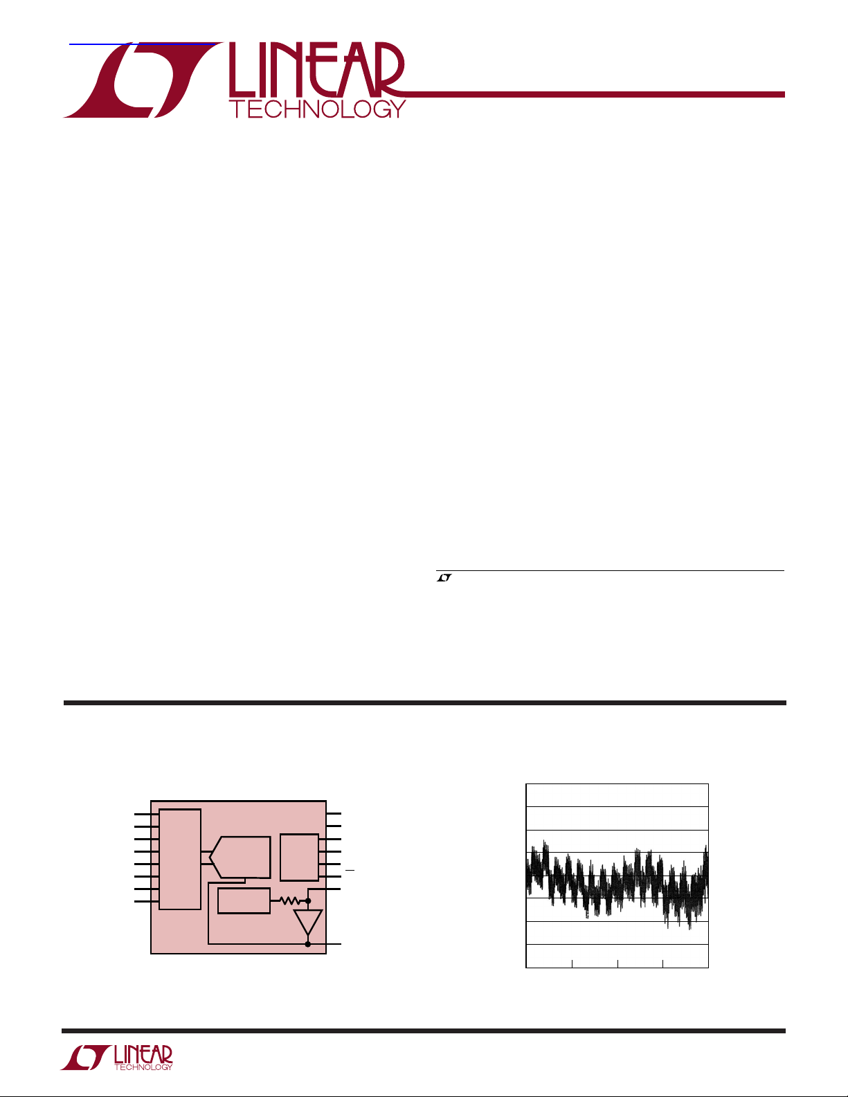
BLOCK DIAGRA
1
CH0
2
CH1
3
CH2
CH3
CH4
CH5
CH6
CH7/COM
4
ANALOG
5
INPUT
6
MUX
7
8
12-/16-BIT
+
200ksps
–
ADC
INTERNAL
2.5V REF
W
LTC1863/LTC1867
SERIAL
PORT
18637 BD
16
15
14
13
12
11
10
9
V
DD
GND
SDI
SDO
SCK
CS/CONV
V
REF
REFCOMP
Integral Nonlinearity vs Output Code
(LTC1867)
2.0
1.5
1.0
0.5
0
INL (LBS)
– 0.5
– 1.0
– 1.5
– 2.0
0
16384 32768 65536
OUTPUT CODE
49152
18637 GO1
18637f
1
LTC1863/LTC1867
WW
W
ABSOLUTE AXI U RATI GS
(Notes 1, 2)
Supply Voltage (VDD)................................... –0.3V to 6V
Analog Input Voltage
CH0-CH7/COM (Note 3) ..........–0.3V to (VDD + 0.3V)
V
, REFCOMP (Note 4).........–0.3V to (VDD + 0.3V)
REF
Digital Input Voltage (SDI, SCK, CS/CONV)
(Note 4) .................................................– 0.3V to 10V
Digital Output Voltage (SDO) .......–0.3V to (VDD + 0.3V)
Power Dissipation.............................................. 500mW
Operating Temperature Range
LTC1863C/LTC1867C/LTC1867AC .......... 0°C to 70°C
LTC1863I/LTC1867I/LTC1867AI ........ –40°C to 85°C
U
PACKAGE/ORDER I FOR ATIO
TOP VIEW
CH0
1
2
CH1
3
CH2
4
CH3
5
CH4
6
CH5
7
CH6
CH7/COM
8
GN PACKAGE
16-LEAD NARROW PLASTIC SSOP
T
= 110°C, θJA = 95°C/W
JMAX
16
15
14
13
12
11
10
9
Storage Temperature Range ................. –65°C to 150°C
Lead Temperature (Soldering, 10 sec)..................300°C
Consult LTC Marketing for parts specified with wider operating temperature ranges.
U
CO VERTER CHARACTERISTICS
temperature range, otherwise specifications are at TA = 25°C. With external reference (Notes 5, 6)
The ● denotes the specifications which apply over the full operating
V
DD
GND
SDI
SDO
SCK
CS/CONV
V
REF
REFCOMP
UUW
ORDER PART
NUMBER
LTC1863CGN
LTC1863IGN
LTC1867CGN
LTC1867IGN
LTC1867ACGN
LTC1867AIGN
GN PART MARKING
1863
1867
LTC1863 LTC1867 LTC1867A
PARAMETER CONDITIONS MIN TYP MAX MIN TYP MAX MIN TYP MAX UNITS
Resolution ● 12 16 16 Bits
No Missing Codes ● 12 15 16 Bits
Integral Linearity Error Unipolar (Note 7) ● ±1 ±4 ±2 LSB
Bipolar ● ±1 ±4 ±2.5 LSB
Differential Linearity Error ● ±1 –2 3 –1 1.75 LSB
Transition Noise 0.1 0.74 0.74 LSB
Offset Error Unipolar (Note 8) ● ±3 ±32 ±32 LSB
Bipolar ● ±4 ±64 ±64 LSB
Offset Error Match Unipolar ±1 ±2 ±2 LSB
Bipolar ±1 ±2 ±2 LSB
Offset Error Drift ±0.5 ±0.5 ±0.5 ppm/°C
Gain Error Unipolar ±6 ±96 ±64 LSB
Bipolar ±6 ±96 ±64 LSB
Gain Error Match ±1 ±4 ±2 LSB
Gain Error Tempco Internal Reference ±15 ±15 ±15 ppm/°C
External Reference ±2.7 ±2.7 ±2.7 ppm/°C
Power Supply Sensitivity VDD = 4.75V – 5.25V ±1 ±5 ±5 LSB
DY A IC ACCURACY
SYMBOL PARAMETER CONDITIONS MIN TYP MAX MIN TYP MAX UNITS
SNR Signal-to-Noise Ratio 1kHz Input Signal 73.6 89 dB
S/(N+D) Signal-to-(Noise + Distortion) Ratio 1kHz Input Signal 73.5 88 dB
U
W
(Note 5)
LTC1863 LTC1867/LTC1867A
RMS
18637f
2
LTC1863/LTC1867
U
W
DY A IC ACCURACY
SYMBOL PARAMETER CONDITIONS MIN TYP MAX MIN TYP MAX UNITS
THD Total Harmonic Distortion 1kHz Input Signal, Up to 5th Harmonic –94.5 – 95 dB
Peak Harmonic or Spurious Noise 1kHz Input Signal –94.5 – 95 dB
Channel-to-Channel Isolation 100kHz Input Signal –100 –117 dB
Full Power Bandwidth –3dB Point 1.25 1.25 MHz
(Note 5)
LTC1863 LTC1867/LTC1867A
UU
A ALOG I PUT
specifications are at TA = 25°C. (Note 5)
SYMBOL PARAMETER CONDITIONS MIN TYP MAX UNITS
Analog Input Range Unipolar Mode (Note 9) ● 0-4.096 V
C
t
IN
ACQ
Analog Input Capacitance for CH0 to Between Conversions (Sample Mode) 32 pF
CH7/COM During Conversions (Hold Mode) 4 pF
Sample-and-Hold Acquisition Time ● 1.5 1.1 µs
Input Leakage Current On Channels, CHX = 0V or V
The ● denotes the specifications which apply over the full operating temperature range, otherwise
LTC1863/LTC1867/LTC1867A
Bipolar Mode
DD
● ±2.048 V
● ±1 µA
UU U
I TER AL REFERE CE CHARACTERISTICS
(Note 5)
LTC1863/LTC1867/LTC1867A
PARAMETER CONDITIONS MIN TYP MAX UNITS
V
Output Voltage I
REF
V
Output Tempco I
REF
V
Line Regulation 4.75V ≤ VDD ≤ 5.25V 0.43 mV/V
REF
V
Output Resistance I
REF
REFCOMP Output Voltage I
= 0 2.480 2.500 2.520 V
OUT
= 0 ±15 ppm/°C
OUT
≤0.1mA 6 kΩ
OUT
= 0 4.096 V
OUT
UU
DIGITAL I PUTS A D DIGITAL OUTPUTS
full operating temperature range, otherwise specifications are at TA = 25°C. (Note 5)
SYMBOL PARAMETER CONDITIONS MIN TYP MAX UNITS
V
IH
V
IL
I
IN
C
IN
V
OH
V
OL
I
SOURCE
I
SINK
High Level Input Voltage VDD = 5.25V ● 2.4 V
Low Level Input Voltage VDD = 4.75V ● 0.8 V
Digital Input Current VIN = 0V to V
Digital Input Capacitance 2pF
High Level Output Voltage (SDO) VDD = 4.75V, IO = –10µA 4.75 V
= 4.75V, IO = –200µA ● 4 4.74 V
V
DD
Low Level Output Voltage (SDO) VDD = 4.75V, IO = 160µA 0.05 V
V
= 4.75V, IO = 1.6mA ● 0.10 0.4 V
DD
Output Source Current SDO = 0V –32 mA
Output Sink Current SDO = V
Hi-Z Output Leakage CS/CONV = High, SDO = 0V or V
Hi-Z Output Capacitance CS/CONV = High (Note 10)
Data Format Unipolar Straight Binary
DD
Bipolar Two’s Complement
The ● denotes the specifications which apply over the
LTC1863/LTC1867/LTC1867A
DD
DD
● ±10 µA
19 mA
● ±10 µA
● 15 pF
18637f
3
LTC1863/LTC1867
WU
POWER REQUIRE E TS
range, otherwise specifications are at TA = 25°C. (Note 5)
SYMBOL PARAMETER CONDITIONS MIN TYP MAX UNITS
V
I
DD
P
DD
DISS
Supply Voltage (Note 9) 4.75 5.25 V
Supply Current f
Power Dissipation ● 6.5 9 mW
The ● denotes the specifications which apply over the full operating temperature
LTC1863/LTC1867/LTC1867A
= 200ksps ● 1.3 1.8 mA
SAMPLE
NAP Mode 150 µA
SLEEP Mode ● 0.2 3 µA
UW
TI I G CHARACTERISTICS
range, otherwise specifications are at TA = 25°C. (Note 5)
SYMBOL PARAMETER CONDITIONS MIN TYP MAX UNITS
f
SAMPLE
t
CONV
t
ACQ
f
SCK
t
1
t
2
t
3
t
4
t
5
t
6
t
7
t
8
Note 1: Absolute Maximum Ratings are those values beyond which the life
of a device may be impaired.
Note 2: All voltage values are with respect to GND (unless otherwise
noted).
Note 3: When these pin voltages are taken below GND or above V
will be clamped by internal diodes. This product can handle input currents
of greater than 100mA without latchup.
Note 4: When these pin voltages are taken below GND, they will be
clamped by internal diodes. This product can handle input currents of
greater than 100mA below GND without latchup. These pins are not
clamped to VDD.
Note 5: VDD = 5V, f
– = 2.5V for bipolar mode unless otherwise specified.
V
IN
Maximum Sampling Frequency ● 200 kHz
Conversion Time ● 3 3.5 µs
Acquisition Time ● 1.5 1.1 µs
SCK Frequency 40 MHz
CS/CONV High Time Short CS/CONV Pulse Mode ● 40 100 ns
SDO Valid After SCK↓ CL = 25pF (Note 11) ● 13 22 ns
SDO Valid Hold Time After SCK↓ CL = 25pF ● 511 ns
SDO Valid After CS/CONV↓ CL = 25pF ● 10 30 ns
SDI Setup Time Before SCK↑ ● 15 –6 ns
SDI Hold Time After SCK↑ ● 10 4 ns
SLEEP Mode Wake-Up Time C
Bus Relinquish Time After CS/CONV↑ CL = 25pF ● 20 40 ns
= 200ksps at 25°C, tr = tf = 5ns and
SAMPLE
The ● denotes the specifications which apply over the full operating temperature
LTC1863/LTC1867/LTC1867A
REFCOMP
, they
DD
= 10µF, C
= 2.2µF60ms
VREF
Note 6: Linearity, offset and gain error specifications apply for both
unipolar and bipolar modes. The INL and DNL are tested in bipolar mode.
Note 7: Integral nonlinearity is defined as the deviation of a code from a
straight line passing through the actual endpoints of the transfer curve.
The deviation is measured from the center of the quantization band.
Note 8: Unipolar offset is the offset voltage measured from +1/2LSB
when␣ the output code flickers between 0000 0000 0000 0000 and
0000 0000 0000␣ 0001 for LTC1867 and between 0000 0000 0000 and
0000 0000 0001 for LTC1863. Bipolar offset is the offset voltage
measured from –1/2LSB when output code flickers between 0000 0000
0000 0000 and 1111 1111 1111 1111 for LTC1867, and between
0000 0000 0000 and 1111 1111 1111 for LTC1863.
Note 9: Recommended operating conditions. The input range of ±2.048V
for bipolar mode is measured with respect to V
Note 10: Guaranteed by design, not subject to test.
Note 11: t2 of 25ns maximum allows f
with 50% duty cycle and f
setup time for the receiving logic).
SCK
SCK
up to 40MHz for falling capture (with 3ns
– = 2.5V.
IN
up to 20MHz for rising capture
4
18637f
UW
TYPICAL PERFOR A CE CHARACTERISTICS
LTC1863/LTC1867
(LTC1867)
Integral Nonlinearity vs
Output Code
2.0
1.5
1.0
0.5
0
INL (LSB)
– 0.5
– 1.0
– 1.5
– 2.0
0
16384 32768 65536
OUTPUT CODE
4096 Points FFT Plot (fIN = 1kHz)
0
–20
–40
–60
–80
AMPLITUDE (dB)
–100
–120
SNR = 88.8dB
SINAD = 87.9dB
THD = 95dB
f
SAMPLE
INTERNAL REFERENCE
49152
= 200ksps
18637 GO1
Differential Nonlinearity vs
Output Code
2.0
1.5
1.0
0.5
0
DNL (LSB)
– 0.5
– 1.0
– 1.5
– 2.0
0
OUTPUT CODE
4096 Points FFT Plot (fIN = 1kHz,
REFCOMP = External 5V)
0
–20
–40
–60
–80
AMPLITUDE (dB)
–100
–120
SNR = 90dB
SINAD = 88.5dB
THD = 94dB
f
SAMPLE
V
REF
REFCOMP = EXT 5V
4915216384 32768 65536
18637 GO2
= 200ksps
= 0V
Histogram for 4096 Conversions
2500
2000
1500
COUNTS
1000
500
0
1
–4
935
276
26
–2–3
Crosstalk vs Input Frequency
–80
–90
–100
–110
–120
SELECTED CHANNEL (dB)
RESULTING AMPLITUDE ON
–130
ADJACENT PAIR
2152
579
122
0–1
CODE
NONADJACENT PAIR
5
321
0
4
18637 GO3
–140
25 50 100
0
FREQUENCY (kHz)
Signal-to-Noise Ratio vs
Frequency
100
90
80
70
60
50
AMPLITUDE (dB)
40
30
20
1
INPUT FREQUENCY (kHz)
75
18637 G04
10 100
18637 G07
–140
25 50 100
0
FREQUENCY (kHz)
Signal-to-(Noise + Distortion) vs
Input Frequency
100
90
80
70
60
50
AMPLITUDE (dB)
40
30
20
1
INPUT FREQUENCY (kHz)
10 100
75
18637 G05
–140
1
ACTIVE CHANNEL INPUT FREQUENCY (kHz)
10 100 1000
18637 G06
Total Harmonic Distortion vs
Input Frequency
–20
–30
–40
–50
–60
–70
AMPLITUDE (dB)
–80
–90
–100
1
INPUT FREQUENCY (kHz)
18637 G08
10 100
18637 G09
18637f
5

LTC1863/LTC1867
UW
TYPICAL PERFOR A CE CHARACTERISTICS
(LTC1863/LTC1867)
Supply Current vs f
2.0
VDD = 5V VDD = 5V
1.5
1.0
SUPPLY CURRENT (mA)
0.5
0
1
10 100 1000
f
SAMPLE
SAMPLE
(ksps)
18637 G10
Integral Nonlinearity vs Output
Code (LTC1863)
1.0
0.8
0.6
0.4
0.2
0
INL (LBS)
–0.2
–0.4
–0.6
–0.8
–1.0
0
512 1536
1024
2048
OUTPUT CODE
Supply Current vs Supply Voltage Supply Current vs Temperature
1.5
= 200ksps
f
SAMPLE
1.4
1.3
1.2
SUPPLY CURRENT (mA)
1.1
1.0
4.5
4.75
SUPPLY VOLTAGE (V)
5.0
5.25
5.5
18637 G11
1.5
VDD = 5V
= 200ksps
f
SAMPLE
1.4
1.3
1.2
SUPPLY CURRENT (mA)
1.1
1.0
–50
02550
–25
TEMPERATURE (°C)
Differential Nonlinearity vs
Output Code (LTC1863)
1.0
0.8
0.6
0.4
0.2
0
–0.2
DNL (LBS)
–0.4
–0.6
–0.8
2560
3072
3584
18637 G13
4096
–1.0
0
512 1536
1024
2048
OUTPUT CODE
2560
3072
3584
18637 G14
4096
75 100
18637 G12
6
18637f

LTC1863/LTC1867
U
UU
PI FU CTIO S
CHO-CH7/COM (Pins 1-8): Analog Input Pins. Analog
inputs must be free of noise with respect to GND. CH7/
COM can be either a separate channel or the common
minus input for the other channels.
REFCOMP (Pin 9): Reference Buffer Output Pin. Bypass to
GND with 10µF tantalum capacitor in parallel with 0.1µF
ceramic capacitor (4.096V Nominal). To overdrive
REFCOMP, tie V
V
(Pin 10): 2.5V Reference Output. This pin can also be
REF
to GND.
REF
used as an external reference buffer input for improved
accuracy and drift. Bypass to GND with 2.2µF tantalum
capacitor in parallel with 0.1µF ceramic capacitor.
CS/CONV (Pin 11): This input provides the dual function
of initiating conversions on the ADC and also frames the
serial data transfer.
UUU
U
U
TYPICAL CO ECTIO DIAGRA
SCK (Pin 12): Shift Clock. This clock synchronizes the
serial data transfer.
SDO (Pin 13): Digital Data Output. The A/D conversion
result is shifted out of this output. Straight binary format
for unipolar mode and two’s complement format for
bipolar mode.
SDI (Pin 14): Digital Data Input Pin. The A/D configuration
word is shifted into this input.
GND (Pin 15): Analog and Digital GND.
VDD (Pin 16): Analog and Digital Power Supply. Bypass to
GND with 10µF tantalum capacitor in parallel with 0.1µF
ceramic capacitor.
TEST CIRCUITS
Load Circuits for Access Timing Load Circuits for Output Float Delay
3k
+
±2.048V
DIFFERENTIAL
INPUTS
4.096V
SINGLE-ENDED
INPUT
5V
3k
DNDN
C
L
C
CH0
CH1
–
CH2
LTC1863/
CH3
LTC1867
+
CH4
CH5
CH6
CH7/COM
L
V
GND
SDI
SDO
SCK
CS/CONV
V
REF
REFCOMP
DD
5V
DIGITAL
I/O
4.096V
10µF
2.5V
2.2µF
18637 TCD
5V
3k
DNDN
3k
C
L
C
L
(A) Hi-Z TO VOH AND VOL TO V
(B) Hi-Z TO VOL AND VOH TO V
OH
OL
18637 TC01
(A) VOH TO Hi-Z
(B) VOL TO Hi-Z
18637 TC02
18637f
7

LTC1863/LTC1867
WUW
TI I G DIAGRA S
t
(For Short Pulse Mode)
1
t
1
CS/CONV
50%
50%
(SDO Valid Before SCK↑),
t
2
t
(SDO Valid Hold Time After SCK↓)
3
SCK
0.4V
t
t
2
3
CS/CONV
SDO
SCK
CS/CONV
t4 (SDO Valid After CONV↓)
t
4
0.4V
Hi-Z
2.4V
0.4V
t7 (SLEEP Mode Wake-Up Time)
t
7
50%
SLEEP BIT (SLP = 0)
READ-IN
50%
SCK
SDI
CS/CONV
SDO
SDO
t5 (SDI Setup Time Before SCK↑),
t
(SDI Hold Time After SCK↑)
6
t
5
2.4V
2.4V
0.4V
t8 (BUS Relinquish Time)
t
8
2.4V
90%
10%
2.4V
0.4V
t
6
2.4V
0.4V
Hi-Z
1867 TD
WUUU
APPLICATIO S I FOR ATIO
Overview
The LTC1863/LTC1867 are complete, low power multiplexed ADCs. They consist of a 12-/16-bit, 200ksps capacitive successive approximation A/D converter, a precision internal reference, a configurable 8-channel analog
input multiplexer (MUX) and a serial port for data transfer.
Conversions are started by a rising edge on the CS/CONV
input. Once a conversion cycle has begun, it cannot be
restarted. Between conversions, the ADCs receive an input
word for channel selection and output the conversion
result, and the analog input is acquired in preparation for
the next conversion. In the acquire phase, a minimum time
of 1.5µs will provide enough time for the sample-and-hold
capacitors to acquire the analog signal.
8
During the conversion, the internal differential 16-bit
capacitive DAC output is sequenced by the SAR from the
most significant bit (MSB) to the least significant bit
(LSB). The input is sucessively compared with the binary
weighted charges supplied by the differential capacitive
DAC. Bit decisions are made by a low-power, differential
comparator. At the end of a conversion, the DAC output
balances the analog input. The SAR contents (a 12-/16-bit
data word) that represent the analog input are loaded into
the 12-/16-bit output latches.
18637f

WUUU
WUUU
APPLICATIO S I FOR ATIO
APPLICATIO S I FOR ATIO
LTC1863/LTC1867
Analog Input Multiplexer
The analog input multiplexer is controlled by a 7-bit input
data word. The input data word is defined as follows:
SD OS S1 S0 COM UNI SLP
SD = SINGLE/DIFFERENTIAL BIT
OS = ODD/SIGN BIT
S1 = ADDRESS SELECT BIT 1
S0 = ADDRESS SELECT BIT 0
COM = CH7/COM CONFIGURATION BIT
UNI = UNIPOLAR/BIPOLAR BIT
SLP = SLEEP MODE BIT
Examples of Multiplexer Options
8 Single-Ended
CH0
+
CH1
+
CH2
+
CH3
+
CH4
+
CH5
+
CH6
+
CH7/COM
+
GND (–)
Combinations of Differential
and Single-Ended
+
–
–
+
+
+
+
+
CH0
{
CH1
CH2
{
CH3
CH4
CH5
CH6
CH7/COM
GND (–)
18637 AI01
+
(–)
{
(+)
–
+
(–)
{
(+)
–
+
(–)
{
(+)
–
+
(–)
{
(+)
–
7 Single-Ended
+
+
+
+
+
+
+
4 Differential
CH0
CH1
CH2
CH3
CH4
CH5
CH6
CH7/COM
to CH7/COM
CH0
CH1
CH2
CH3
CH4
CH5
CH6
CH7/COM (–)
Changing the MUX Assignment “On the Fly”
1st Conversion 2nd Conversion
+
–
+
–
CH2
{
CH3
CH4
{
CH5
CH7/COM
(UNUSED)
–
+
+
+
{
{
CH2
CH3
CH4
CH5
CH7/COM (–)
18637 AI02
Tables 1 and 2 show the configurations when COM = 0,
and COM = 1.
Table 1. Channel Configuration (When COM = 0, CH7/COM Pin
Is Used as CH7)
Channel Configuration
SD OS S1 S0 COM “+” “-”
00000 CH0 CH1
00010 CH2 CH3
00100 CH4 CH5
00110 CH6 CH7
01000 CH1 CH0
01010 CH3 CH2
01100 CH5 CH4
01110 CH7 CH6
10000 CH0 GND
10010 CH2 GND
10100 CH4 GND
10110 CH6 GND
11000 CH1 GND
11010 CH3 GND
11100 CH5 GND
11110 CH7 GND
Table 2. Channel Configuration (When COM = 1, CH7/COM Pin
Is Used as COMMON)
Channel Configuration
SD OS S1 S0 COM "+" "-"
10001 CH0 CH7/COM
10011 CH2 CH7/COM
10101 CH4 CH7/COM
10111 CH6 CH7/COM
11001 CH1 CH7/COM
11011 CH3 CH7/COM
11101 CH5 CH7/COM
18637f
9

LTC1863/LTC1867
WUUU
APPLICATIO S I FOR ATIO
Driving the Analog Inputs
The analog inputs of the LTC1863/LTC1867 are easy to
drive. Each of the analog inputs can be used as a singleended input relative to the GND pin (CH0-GND, CH1-GND,
etc) or in pairs (CH0 and CH1, CH2 and CH3, CH4 and CH5,
CH6 and CH7) for differential inputs. In addition, CH7 can
act as a COM pin for both single-ended and differential
modes if the COM bit in the input word is high. Regardless
of the MUX configuration, the “+” and “–” inputs are
sampled at the same instant. Any unwanted signal that is
common mode to both inputs will be reduced by the
common mode rejection of the sample-and-hold circuit.
The inputs draw only one small current spike while charging the sample-and-hold capacitors during the acquire
mode. In conversion mode, the analog inputs draw only a
small leakage current. If the source impedance of the
driving circuit is low then the LTC1863/LTC1867 inputs
can be driven directly. More acquisition time should be
allowed for a higher impedance source.
The following list is a summary of the op amps that are
suitable for driving the LTC1863/LTC1867. More detailed
information is available in the Linear Technology data
books or Linear Technology website.
LT1007 - Low noise precision amplifier. 2.7mA supply
current ±5V to ±15V supplies. Gain bandwidth product
8MHz. DC applications.
LT1097 - Low cost, low power precision amplifier. 300µA
supply current. ±5V to ±15V supplies. Gain bandwidth
product 0.7MHz. DC applications.
LT1227 - 140MHz video current feedback amplifier. 10mA
supply current. ±5V to ±15V supplies. Low noise and low
distortion.
LT1360 - 37MHz voltage feedback amplifier. 3.8mA supply current. ±5V to ±15V supplies. Good AC/DC specs.
LT1363 - 50MHz voltage feedback amplifier. 6.3mA supply current. Good AC/DC specs.
LT1364/LT1365 - Dual and quad 50MHz voltage feedback
amplifiers. 6.3mA supply current per amplifier. Good
AC/DC specs.
LT1468 - 90MHz, 22V/µs 16-bit accurate amplifier
LT1469 - Dual LT1468
Input Filtering
The noise and the distortion of the input amplifier and
other circuitry must be considered since they will add to
the LTC1863/LTC1867 noise and distortion. Noisy input
circuitry should be filtered prior to the analog inputs to
minimize noise. A simple 1-pole RC filter is sufficient for
many applications. For instance, Figure 1 shows a 50Ω
source resistor and a 2000pF capacitor to ground on the
input will limit the input bandwidth to 1.6MHz. The source
impedance has to be kept low to avoid gain error and
degradation in the AC performance. The capacitor also
acts as a charge reservoir for the input sample-and-hold
and isolates the ADC input from sampling glitch sensitive
circuitry. High quality capacitors and resistors should be
used since these components can add distortion. NPO and
silver mica type dielectric capacitors have excellent linearity. Carbon surface mount resistors can also generate
distortion from self heating and from damage that may
occur during soldering. Metal film surface mount resistors are much less susceptible to both problems.
10
18637f

WUUU
APPLICATIO S I FOR ATIO
LTC1863/LTC1867
ANALOG
INPUT
50Ω
2000pF
10µF
CH0
LTC1863/
LTC1867
GND
REFCOMP
1867 F01a
Figure 1a. Optional RC Input Filtering for Single-Ended Input
1000pF
1000pF
1000pF
10µF
CH0
LTC1863/
LTC1867
CH1
REFCOMP
1867 F01b
DIFFERENTIAL
ANALOG
INPUTS
50Ω
50Ω
Figure 1b. Optional RC Input Filtering for Differential Inputs
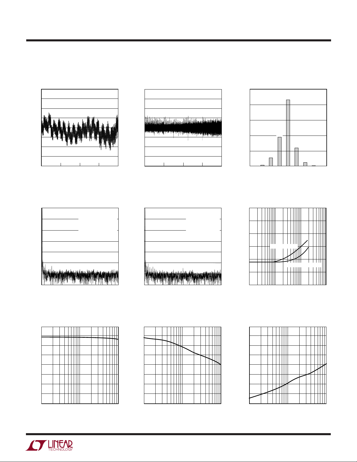
DC Performance
One way of measuring the transition noise associated with
a high resolution ADC is to use a technique where a DC
signal is applied to the input of the ADC and the resulting
output codes are collected over a large number of conversions. For example, in Figure 2 the distribution of output
codes is shown for a DC input that had been digitized 4096
times. The distribution is Gaussian and the RMS code
transition noise is about 0.74LSB.
2500
2152
2000
Dynamic Performance
FFT (Fast Fourier Transform) test techniques are used to
test the ADC’s frequency response, distortion and noise at
the rated throughput. By applying a low distortion sine
wave and analyzing the digital output using an FFT algorithm, the ADC’s spectral content can be examined for
frequencies outside the fundamental.
Signal-to-Noise Ratio
The Signal-to-Noise and Distortion Ratio (SINAD) is the
ratio between the RMS amplitude of the fundamental input
frequency to the RMS amplitude of all other frequency
components at the A/D output. The output is band limited
to frequencies from above DC and below half the sampling
frequency. Figure 3 shows a typical SINAD of 87.9dB with
a 200kHz sampling rate and a 1kHz input. When an
external 5V is applied to REFCOMP (tie V
to GND), a
REF
signal-to-noise ratio of 90dB can be achieved.
0
–20
–40
–60
–80
AMPLITUDE (dB)
–100
–120
–140
25 50 100
0
Figure 3. LTC1867 Nonaveraged 4096 Point FFT Plot
SNR = 88.8dB
SINAD = 87.9dB
THD = 95dB
f
SAMPLE
INTERNAL REFERENCE
FREQUENCY (kHz)
= 200ksps
75
18637 G04
1500
COUNTS
1000
500
0
1
–4
935
579
276
26
–2–3
CODE
122
5
0
0–1
321
4
18637 GO3
Figure 2. LTC1867 Histogram for 4096 Conversions
Total Harmonic Distortion
Total Harmonic Distortion (THD) is the ratio of the RMS
sum of all harmonics of the input signal to the fundamental
itself. The out-of-band harmonics alias into the frequency
band between DC and half the sampling frequency. THD is
expressed as:
2
2
22
...
4
V
1
N
18637f
THD
VVV V
++ +
2
=
20
log
3
11

LTC1863/LTC1867
WUUU
APPLICATIO S I FOR ATIO
where V1 is the RMS amplitude of the fundamental frequency and V2 through VN are the amplitudes of the
second through Nth harmonics.
Internal Reference
The LTC1863/LTC1867 has an on-chip, temperature compensated, curvature corrected, bandgap reference that is
factory trimmed to 2.5V. It is internally connected to a
reference amplifier and is available at V
(Pin 10). A 6k
REF
resistor is in series with the output so that it can be easily
overdriven by an external reference if better drift and/or
accuracy are required as shown in Figure 4. The reference
amplifier gains the V
voltage by 1.638V to 4.096V at
REF
REFCOMP (Pin 9). This reference amplifier compensation
pin, REFCOMP, must be bypassed with a 10µF ceramic or
tantalum in parallel with a 0.1µF ceramic for best noise
performance.
R1
2.5V
4.096V
V
10
REF
2.2µF
REFCOMP
10µF
9
GND
15
REFERENCE
R2
R3
AMP
Figure 4a. LT1867 Reference Circuit
5V
6k
BANDGAP
REFERENCE
LTC1863/LTC1867
1867 F04a
Digital Interface
The LTC1863/LTC1867 have very simple digital interface
that is enabled by the control input, CS/CONV. A logic
rising edge applied to the CS/CONV input will initiate a
conversion. After the conversion, taking CS/CONV low will
enable the serial port and the ADC will present digital data
in two’s complement format in bipolar mode or straight
binary format in unipolar mode, through the SCK/SDO
serial port.
Internal Clock
The internal clock is factory trimmed to achieve a typical
conversion time of 3µs and a maximum conversion time,
3.5µs, over the full operating temperature range. The
typical acquisition time is 1.1µs, and a throughput sam-
pling rate of 200ksps is tested and guaranteed.
Automatic Nap Mode
The LTC1863/LTC1867 go into automatic nap mode when
CS/CONV is held high after the conversion is complete.
With a typical operating current of 1.3mA and automatic
150µA nap mode between conversions, the power dissi-
pation drops with reduced sample rate. The ADC only
keeps the V
and REFCOMP voltages active when the
REF
part is in the automatic nap mode. The slower the sample
rate allows the power dissipation to be lower (see
Figure 5).
2.0
VDD = 5V
1.5
V
IN
LT1019A-2.5
V
OUT
+
2.2µF
0.1µF10µF
10
9
15
V
REF
LTC1863/
LTC1867
REFCOMP
GND
1867 F04b
Figure 4b. Using the LT1019-2.5 as an External Reference
12
1.0
SUPPLY CURRENT (mA)
0.5
0
1
10 100 1000
f
(ksps)
SAMPLE
Figure 5. Supply Current vs f
18637 G10
SAMPLE
18637f

WUUU
APPLICATIO S I FOR ATIO
LTC1863/LTC1867
If the CS/CONV returns low during a bit decision, it can
create a small error. For best performance ensure that the
CS/CONV returns low either within 100ns after the conversion starts (i.e. before the first bit decision) or after the
conversion ends. If CS/CONV is low when the conversion
ends, the MSB bit will appear on SDO at the end of the
conversion and the ADC will remain powered up.
Sleep Mode
If the SLP = 1 is selected in the input word, the ADC will
enter SLEEP mode and draw only leakage current (provided that all the digital inputs stay at GND or VDD). After
release from the SLEEP mode, the ADC need 60ms to wake
up (2.2µF/10µF bypass capacitors on V
/REFCOMP
REF
pins).
Broad Layout and Bypassing
To obtain the best performance, a printed circuit board
with a ground plane is required. Layout for the printed
circuit board should ensure digital and analog signal lines
are separated as much as possible. In particular, care
should be taken not to run any digital signal alongside an
analog signal.
All analog inputs should be screened by GND. V
REF
,
REFCOMP and VDD should be bypassed to this ground
plane as close to the pin as possible; the low impedance of
the common return for these bypass capacitors is essential to the low noise operation of the ADC. The width for
these tracks should be as wide as possible.
Timing and Control
Conversion start is controlled by the CS/CONV digital
input. The rising edge transition of the CS/CONV will start
a conversion. Once initiated, it cannot be restarted until the
conversion is complete. Figures 6 and 7 show the timing
diagrams for two types of CS/CONV pulses.
Example 1 (Figure 6) shows the LTC1863/LTC1867 operating in automatic nap mode with CS/CONV signal staying
HIGH after the conversion. Automatic nap mode provides
power reduction at reduced sample rate. The ADCs can
also operate with the CS/CONV signal returning LOW
before the conversion ends. In this mode (Example 2,
Figure 7), the ADCs remain powered up.
Figures 8 and 9 are the transfer characteristics for the
bipolar and unipolar mode.
1/f
CS/CONV
SCK
SDI
SDO
(LTC1863)
SDO
(LTC1867)
Figure 6. Example 1, CS/CONV Starts a Conversion and Remains HIGH Until Next Data Transfer. With CS/CONV Remaining HIGH after
Hi-Z
Hi-Z
t
CONV
the Conversion, Automatic Nap Modes Provides Power Reduction at Reduced Sample Rate.
NAP MODE
12345678910111213141516
COM
S0SD 0S S1
MSB
D11 D10 D9 D8 D7 D6 D5 D4 D3 D2 D1 D0
MSB
D12D15 D14 D13 D11 D10 D9 D8 D7 D6 D5 D4 D3 D2 D1 D0
UNI SLP
SCK
NOT NEEDED FOR LTC1863
DON'T CAREDON'T CARE
1867 F06
18637f
13

LTC1863/LTC1867
U
WUU
APPLICATIO S I FOR ATIO
CS/CONV
SCK
SDI
SDO
(LTC1863)
SDO
(LTC1867)
t
CONV
Hi-Z
t
CONV
Hi-Z
With CS/CONV Returning LOW Before the Conversion, the ADC Remains Powered Up.
011...111
011...110
000...001
000...000
111...111
111...110
100...001
OUTPUT CODE (TWO’S COMPLIMENT)
100...000
12345678910111213141516
S0SD 0S S1 COM UNI SLP
MSB = D11 D10 D9 D8 D7 D6 D5 D4 D3 D2 D1 D0
D12MSB = D15 D14 D13 D11 D10 D9 D8 D7 D6 D5 D4 D3 D2 D1 D0
Figure 7. Example 2, CS/CONV Starts a Conversion with Short Active HIGH Pulse.
BIPOLAR
ZERO
FS = 4.096
n
1LSB = FS/2
1LSB = (LTC1863) = 1mV
1LSB = (LTC1867) = 62.5µV
–1
0V
1
LSB
FS/2 – 1LSB–FS/2
1867 F08
LSB
INPUT VOLTAGE (V)
t
ACQ
NOT NEEDED FOR LTC1863
111...111
111...110
100...001
100...000
011...111
011...110
OUTPUT CODE
000...001
000...000
UNIPOLAR
ZERO
DON'T CAREDON'T CARE
FS = 4.096
n
1LSB = FS/2
1LSB = (LTC1863) = 1mV
1LSB = (LTC1867) = 62.5µV
INPUT VOLTAGE (V)
1867 F07
FS – 1LSB0V
1867 F09
14
Figure 8. LTC1863/LTC1867 Bipolar Transfer
Characteristics (Two’s Complement)
Figure 9. LTC1863/LTC1867 Unipolar Transfer
Characteristics (Straight Binary)
18637f

PACKAGE DESCRIPTIO
LTC1863/LTC1867
U
GN Package
16-Lead Plastic SSOP (Narrow .150 Inch)
(Reference LTC DWG # 05-08-1641)
.045 ±.005
.254 MIN
RECOMMENDED SOLDER PAD LAYOUT
.007 – .0098
(0.178 – 0.249)
.016 – .050
NOTE:
1. CONTROLLING DIMENSION: INCHES
2. DIMENSIONS ARE IN
3. DRAWING NOT TO SCALE
*DIMENSION DOES NOT INCLUDE MOLD FLASH. MOLD FLASH
SHALL NOT EXCEED 0.006" (0.152mm) PER SIDE
**DIMENSION DOES NOT INCLUDE INTERLEAD FLASH. INTERLEAD
FLASH SHALL NOT EXCEED 0.010" (0.254mm) PER SIDE
(0.406 – 1.270)
INCHES
(MILLIMETERS)
.150 – .165
.0250 BSC.0165 ±.0015
.015
(0.38 ± 0.10)
0° – 8° TYP
± .004
× 45°
.229 – .244
(5.817 – 6.198)
.0532 – .0688
(1.35 – 1.75)
.008 – .012
(0.203 – 0.305)
TYP
16
15
12
.189 – .196*
(4.801 – 4.978)
14
12 11 10
13
5
4
3
678
.0250
(0.635)
BSC
.009
(0.229)
9
.150 – .157**
(3.810 – 3.988)
.004 – .0098
(0.102 – 0.249)
GN16 (SSOP) 0204
REF
Information furnished by Linear Technology Corporation is believed to be accurate and reliable.
However, no responsibility is assumed for its use. Linear Technology Corporation makes no representation that the interconnection of its circuits as described herein will not infringe on existing patent rights.
18637f
15

LTC1863/LTC1867
RELATED PARTS
PART NUMBER DESCRIPTION COMMENTS
LTC1417 14-Bit, 400ksps Serial ADC 20mW, Unipolar or Bipolar, Internal Reference, SSOP-16 Package
LT1460 Micropower Precision Series Reference Bandgap, 130µA Supply Current, 10ppm/°C, SOT-23 Package
LT1468/LT1469 Single/Dual 90MHz, 22V/µs, 16-Bit Accurate Op Amps Low Input Offset: 75µV/125µV
LTC1609 16-Bit, 200ksps Serial ADC 65mW, Configurable Bipolar and Unipolar Input Ranges, 5V Supply
LT1790 Micropower Low Dropout Reference 60µA Supply Current, 10ppm/°C, SOT-23 Package
LTC1850/LTC1851 10-Bit/12-Bit, 8-Channel, 1.25Msps ADC Parallel Output, Programmable MUX and Sequencer, 5V Supply
LTC1852/LTC1853 10-Bit/12-Bit, 8-Channel, 400ksps ADC Parallel Output, Programmable MUX and Sequencer, 3V or 5V Supply
LTC1860/LTC1861 12-Bit, 1-/2-Channel 250ksps ADC in MSOP 850µA at 250ksps, 2µA at 1ksps, SO-8 and MSOP Packages
LTC1860L/LTC1861L 3V, 12-Bit, 1-/2-Channel 150ksps ADC 450µA at 150ksps, 10µA at 1ksps, SO-8 and MSOP Packages
LTC1864/LTC1865 16-Bit, 1-/2-Channel 250ksps ADC in MSOP 850µA at 250ksps, 2µA at 1ksps, SO-8 and MSOP Packages
LTC1864L/LTC1865L 3V, 16-Bit, 1-/2-Channel 150ksps ADC in MSOP 450µA at 150ksps, 10µA at 1ksps, SO-8 and MSOP Packages
16
Linear Technology Corporation
1630 McCarthy Blvd., Milpitas, CA 95035-7417
(408) 432-1900 ● FAX: (408) 434-0507
●
www.linear.com
18637f
LT/TP 0504 1K • PRINTED IN USA
LINEAR TECHNOLOGY CORPORATION 2004
 Loading...