

LTC1821
www.BDTIC.com/LINEAR
16-Bit, Ultra Precise,
FEATURES
■
2µs Settling to 0.0015% for 10V Step
■
1LSB Max DNL and INL Over Industrial
Temperature Range
■
On-Chip 4-Quadrant Resistors Allow Precise 0V to
10V, 0V to –10V or ±10V Outputs
■
Low Glitch Impulse: 2nV•s
■
Low Noise: 13nV/√Hz
■
36-Lead SSOP Package
■
Power-On Reset
■
Asynchronous Clear Pin
LTC1821: Reset to Zero Scale
LTC1821-1: Reset to Midscale
U
APPLICATIO S
■
Process Control and Industrial Automation
■
Precision Instrumentation
■
Direct Digital Waveform Generation
■
Software-Controlled Gain Adjustment
■
Automatic Test Equipment
Fast Settling V
OUT
DAC
U
DESCRIPTIO
The LTC®1821 is a parallel input 16-bit multiplying voltage
output DAC that operates from analog supply voltages of
±5V up to ±15V. INL and DNL are accurate to 1LSB over the
industrial temperature range in both unipolar 0V to 10V and
bipolar ±10V modes. Precise 16-bit bipolar ±10V outputs are
achieved with on-chip 4-quadrant multiplication resistors.
The LTC1821 is available in a 36-lead SSOP package and is
specified over the industrial temperature range.
The device includes an internal deglitcher circuit that reduces
the glitch impulse to less than 2nV•s (typ). The LTC1821
settles to 1LBS in 2µs with a full-scale 10V step. The
combination of fast, precise settling and ultra low glitch make
the LTC1821 ideal for precision industrial control applications.
The asynchronous CLR pin resets the LTC1821 to zero scale
and resets the LTC1821-1 to midscale.
, LTC and LT are registered trademarks of Linear Technology Corporation.
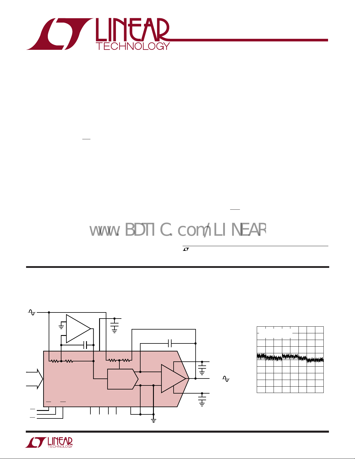
TYPICAL APPLICATIO
16-Bit, 4-Quadrant Multiplying DAC with a
Minimum of External Components
V
REF
–V
REF
DATA
INPUTS
3 TO 6,
25 TO 36
WR
LD
CLR
16
10 9
R1
WR
24 23
3
+
LT®1468
2
–
R
COM
R1
R2
LTC1821-1
LD
CLR
7
6
15pF
8
2
V
REF
CC
DNC*
DNC*
19
18
*DO NOT CONNECT
11
R
DNC*
OFS
R
OFS
16-BIT DAC
21
U
5V
0.1µF
12 14
R
R
FB
DGNDNC AGNDSAGNDF
122
FBIOUT
17 16
LTC1821/LTC1821-1
Integral Nonlinearity
1.0
V
= 10V
REF
0.8
= ±10V BIPOLAR
V
15pF
+
15
V
–
13
+
V
OUT
–
V
20
0.1µF
–15V
0.1µF
15V
V
OUT
1821 TA01
V
REF
=
–V
REF
OUT
0.6
0.4
0.2
0
–0.2
–0.4
–0.6
INTEGRAL NONLINEARITY (LSB)
–0.8
–1.0
0
32768
16384
DIGITAL INPUT CODE
49152
65535
1821 TA02
1
LTC1821
1
2
3
4
5
6
7
8
9
10
11
12
13
14
15
16
17
18
TOP VIEW
GW PACKAGE
36-LEAD PLASTIC SSOP WIDE
36
35
34
33
32
31
30
29
28
27
26
25
24
23
22
21
20
19
D4
D5
D6
D7
D8
D9
D10
D11
D12
D13
D14
D15
WR
LD
NC
DNC*
V
–
DNC*
DGND
V
CC
D3
D2
D1
D0
CLR
REF
R
COM
R1
R
OFS
R
FB
V
OUT
I
OUT
V
+
AGNDS
AGNDF
DNC*
www.BDTIC.com/LINEAR
WW
W
U
ABSOLUTE MAXIMUM RATINGS
(Note 1)
VCC to AGNDF, AGNDS ............................... – 0.3V to 7V
VCC to DGND .............................................. –0.3V to 7V
Total Supply Voltage (V+ to V–) ............................... 36V
AGNDF, AGNDS to DGND ............................. VCC + 0.3V
DGND to AGNDF, AGNDS ............................. VCC + 0.3V
REF, R
R
OFS
Digital Inputs to DGND ............... –0.3V to (VCC + 0.3V)
I
OUT
Maximum Junction Temperature ..........................150°C
Operating Temperature Range
LTC1821C/LTC1821-1C.......................... 0°C to 70°C
LTC1821I/LTC1821-1I ....................... –40°C to 85°C
Storage Temperature Range ................ –65°C to 150°C
Lead Temperature (Soldering, 10 sec)................. 300°C
to AGNDF, AGNDS, DGND .................. ±15V
COM
, RFB, R1, to AGNDF, AGNDS, DGND ............ ±15V
to AGNDF, AGNDS............... –0.3V to (VCC + 0.3V)
U
W
U
PACKAGE/ORDER INFORMATION
ORDER PART
NUMBER
LTC1821ACGW
LTC1821BCGW
LTC1821-1ACGW
LTC1821-1BCGW
LTC1821AIGW
LTC1821BIGW
LTC1821-1AIGW
LTC1821-1BIGW
T
= 125°C, θJA = 80°C/W
JMAX
*DO NOT CONNECT
Consult factory for parts specified with wider operating temperature ranges.
ELECTRICAL CHARACTERISTICS
The ● denotes specifications which apply over the full operating temperature range, otherwise specifications are TA = T
V+ = 15V, V– = –15V, VCC = 5V, V
SYMBOL PARAMETER CONDITIONS MIN TYP MAX MIN TYP MAX UNITS
Accuracy
Resolution ● 16 16 Bits
Monotonicity ● 16 16 Bits
INL Integral Nonlinearity TA = 25°C (Note 2) ±2 ±0.25 ±1LSB
DNL Differential Nonlinearity TA = 25°C ±1 ±0.2 ±1LSB
GE Gain Error Unipolar Mode
PSRR Power Supply Rejection Ratio VCC = 5V ±10% ● 2 0.7 2 LSB/V
2
Gain Temperature Coefficient ∆Gain/∆Temperature (Note 4) ● 1 3 1 3 ppm/°C
Unipolar Zero-Scale Error TA = 25°C ±3 ±0.25 ±2LSB
Bipolar Zero Error TA = 25°C ±12 ±2 ±8LSB
= 10V, AGNDF = AGNDS = DGND = 0V.
REF
T
to T
MIN
MAX
to T
T
MIN
MAX
= 25°C (Note 3) ±16 ±5 ±16 LSB
T
A
T
to T
MIN
MAX
Bipolar Mode
T
= 25°C (Note 3) ±16 ±2 ±16 LSB
A
to T
T
MIN
MAX
to T
T
MIN
MAX
T
to T
MIN
MAX
+
V
, V– = ±4.5V to ±16.5V ● ±2 ±0.1 ±2 LSB/V
MIN
to T
MAX
,
LTC1821B/-1B LTC1821A/-1A
● ±2 ±0.35 ±1LSB
● ±1 ±0.2 ±1LSB
● ±24 ±8 ±16 LSB
● ±24 ±5 ±16 LSB
● ±6 ±0.50 ±4LSB
● ±16 ±3 ±10 LSB

LTC1821
www.BDTIC.com/LINEAR
ELECTRICAL CHARACTERISTICS
The ● denotes specifications which apply over the full operating temperature range, otherwise specifications are TA = T
V+ = 15V, V– = –15V, VCC = 5V, V
SYMBOL PARAMETER CONDITIONS MIN TYP MAX UNITS
Reference Input
R
REF
R1/R2 R1/R2 Resistance (Bipolar) (Notes 6, 11) ● 91220 kΩ
R
OFS
AC Performance (Note 4)
Analog Outputs (Note 4)
V
OUT
I
SC
SR Slew Rate RL = 2k, V+ = 15V, V– = –15V 20 V/µs
Digital Inputs
V
IH
V
IL
I
IN
C
IN
Timing Characteristics
t
DS
t
DH
t
WR
t
LD
t
CLR
t
LWD
Power Supply
I
CC
I
S
V
CC
+
V
–
V
DAC Input Resistance (Unipolar) (Note 6) ● 4.5 6 10 kΩ
, RFBFeedback and Offset Resistances (Note 6) ● 91220 kΩ
Output Voltage Settling Time ∆V
Midscale Glitch Impulse (Note 10) 2 nV•s
Digital-Feedthrough (Note 9) 2 nV•s
Multiplying Feedthrough Error V
Multiplying Bandwidth Code = Full Scale (Note 7) 600 kHz
Output Noise Voltage Density 1kHz to 100kHz (Note 7)
Output Noise Voltage 0.1Hz to 10Hz (Note 7)
1/f Noise Corner (Note 7) 30 Hz
DAC Output Swing RL = 2k, V+ = 15V, V– = –15V ● ±12.6 V
DAC Output Load Regulation V+ = 15V, V– = –15V, ±5mA Load ● 0.02 0.2 LSB/mA
Short-Circuit Current V
Digital Input High Voltage ● 2.4 V
Digital Input Low Voltage ● 0.8 V
Digital Input Current ● 0.001 ±1 µA
Digital Input Capacitance (Note 4 ) VIN = 0V ● 8pF
Data to WR Setup Time ● 60 20 ns
Data to WR Hold Time ● 0–12 ns
WR Pulse Width ● 60 25 ns
LD Pulse Width ● 110 55 ns
Clear Pulse Width ● 60 40 ns
WR to LD Delay Time ● 0ns
Supply Current, V
Supply Current, V+, V
Supply Voltage ● 4.5 5 5.5 V
Supply Voltage ● 4.5 16.5 V
Supply Voltage ● –16.5 –4.5 V
CC
= 10V, AGNDF = AGNDS = DGND = 0V.
REF
= 10V (Notes 7, 8) 2 µs
OUT
= ±10V, 10kHz Sine Wave (Note 7) 1 mV
REF
Code = Zero Scale 13 nV/√Hz
Code = Full Scale 20 nV/√Hz
Code = Zero Scale 0.45 µV
Code = Full Scale 1 µV
RL = 2k, V+ = 5V, V– = –5V ● ±2.6 V
= 0V, V+ = 15V, V– = –15V ● 12 40 mA
OUT
= 2k, V+ = 5V, V– = –5V 14 V/µs
R
L
Digital Inputs = 0V or V
–
±15V ● 4.5 7.0 mA
±5V
CC
● 1.5 10 µA
● 4.0 6.8 mA
MIN
to T
MAX
,
P-P
RMS
RMS
3
LTC1821
www.BDTIC.com/LINEAR
ELECTRICAL CHARACTERISTICS
Note 1: Absolute Maximum Ratings are those values beyond which the life
of a device may be impaired.
Note 2: ±1LSB = ±0.0015% of full scale = ±15.3ppm of full scale.
Note 3: Using internal feedback resistor.
Note 4: Guaranteed by design, not subject to test.
Note 5: I
with DAC register loaded to all 0s.
OUT
Note 6: Typical temperature coefficient is 100ppm/°C.
Note 8: To 0.0015% for a full-scale change, measured from the rising
edge of LD.
Note 9: REF
1s to all 0s. LD low and WR high.
Note 10: Midscale transition code: 0111 1111 1111 1111 to
1000 0000 0000 0000. Unipolar mode, C
Note 11: R1 and R2 are measured between R1 and R
Note 7: Measured in unipolar mode.
UW
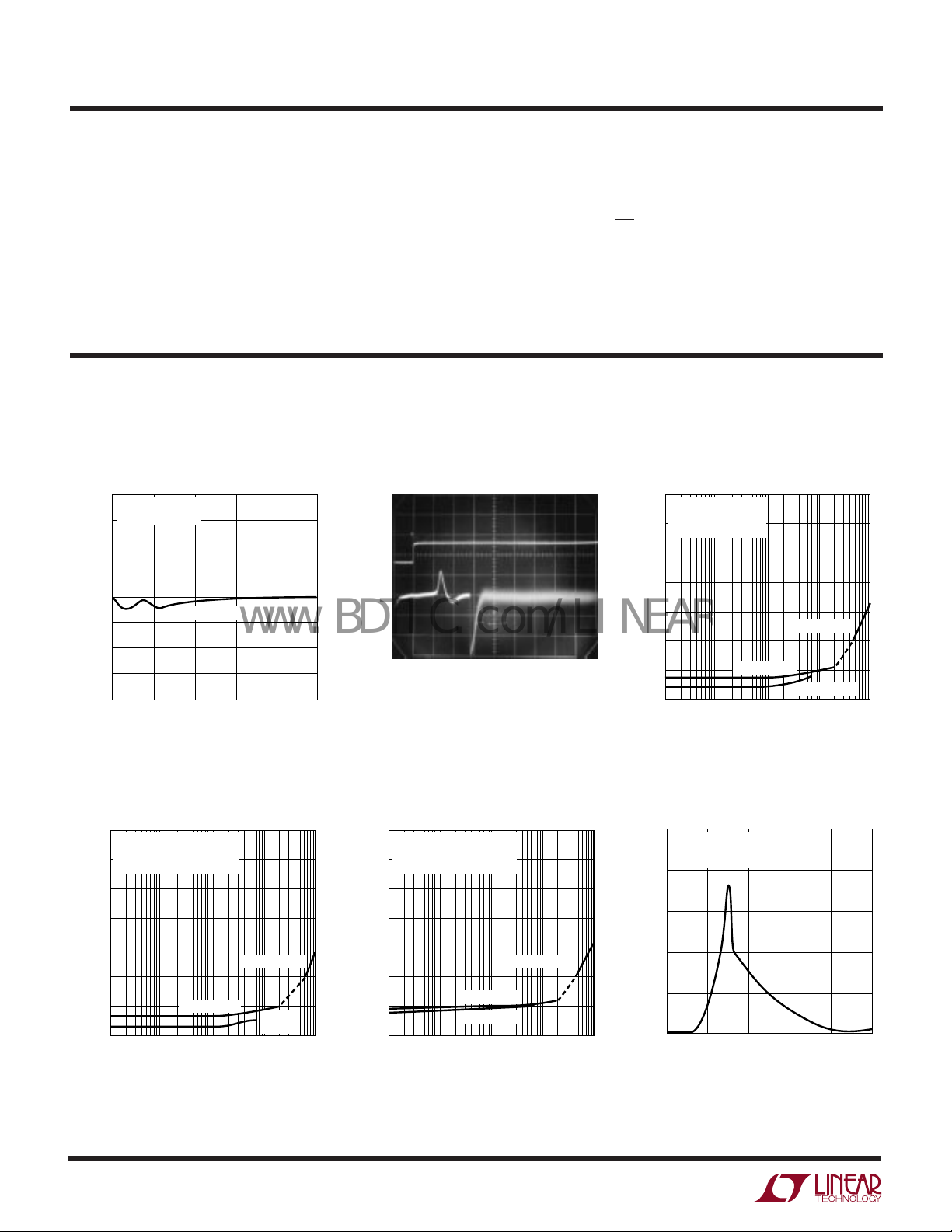
TYPICAL PERFOR A CE CHARACTERISTICS
Midscale Glitch Impulse
40
C
V
30
20
10
0
–10
OUTPUT VOLTAGE (mV)
–20
–30
–40
0
= 30pF
FEEDBACK
= 10V
REF
1nV-s TYPICAL
0.2 0.4 0.8
TIME (µs)
0.6
WAVEFORM
500µV/DIV
1.0
1821 G01
LD PULSE
5V/DIV
GATED
SETTLING
Full-Scale Setting Waveform
V
= –10V
REF
C
FEEDBACK
0V TO 10V STEP
500ns/DIV
= 20pF
= 0V. DAC register contents changed from all 0s to all 1s or all
= 33pF.
FEEDBACK
, REF and R
COM
COM
.
Unipolar Multiplying Mode
Signal-to-(Noise + Distortion)
vs Frequency
–40
VCC = 5V
= 30pF
C
FEEDBACK
–50
1821 G02
REFERENCE = 6V
–60
–70
–80
–90
–100
SIGNAL/(NOISE + DISTORTION) (dB)
–110
10 1k 10k 100k
RMS
500kHz FILTER
80kHz FILTER
30kHz FILTER
100
FREQUENCY (Hz)
1821 G03
Bipolar Multiplying Mode
Signal-to-(Noise + Distortion)
vs Frequency, Code = All Zeros
–40
VCC = 5V USING AN LT1468
= 15pF
C
FEEDBACK
–50
REFERENCE = 6V
–60
–70
–80
–90
–100
SIGNAL/(NOISE + DISTORTION) (dB)
–110
10 1k 10k 100k
RMS
80kHz FILTER
100
FREQUENCY (Hz)
500kHz FILTER
30kHz
FILTER
1821 G04
Bipolar Multiplying Mode
Signal-to-(Noise + Distortion)
vs Frequency, Code = All Ones
–40
VCC = 5V USING AN LT1468
= 15pF
C
FEEDBACK
–50
REFERENCE = 6V
–60
–70
–80
–90
–100
SIGNAL/(NOISE + DISTORTION) (dB)
–110
10 1k 10k 100k
80kHz FILTER
30kHz FILTER
100
FREQUENCY (Hz)
4
RMS
500kHz FILTER
1821 G05
V
Supply Current vs Digital
CC
Input Voltage
5
VCC = 5V
ALL DIGITAL INPUTS
TIED TOGETHER
4
3
2
SUPPLY CURRENT (mA)
1
0
1
0
INTPUT VOLTAGE (V)
3
4
2
5
1821 G06

UW
www.BDTIC.com/LINEAR
TYPICAL PERFOR A CE CHARACTERISTICS
Logic Threshold vs VCC Supply
Voltage
3.0
2.5
2.0
1.5
1.0
LOGIC THRESHOLD (V)
0.5
0
0
234
1
SUPPLY VOLTAGE (V)
576
1821 G07
Integral Nonlinearity (INL) Differential Nonlinearity (DNL)
1.0
0.8
0.6
0.4
0.2
0
–0.2
–0.4
–0.6
INTEGRAL NONLINEARITY (LSB)
–0.8
–1.0
0
16384
32768
DIGITAL INPUT CODE
49152
65535
1821 G08
1.0
0.8
0.6
0.4
0.2
0
–0.2
–0.4
–0.6
DIFFERENTIAL NONLINEARITY (LSB)
–0.8
–1.0
0
16384
32768
DIGITAL INPUT CODE
LTC1821
49152
65535
1821 G09
Integral Nonlinearity vs Reference
Voltage in Unipolar Mode
1.0
0.8
0.6
0.4
0.2
0
–0.2
–0.4
–0.6
INTEGRAL NONLINEARITY (LSB)
–0.8
–1.0
–6
–10
–4
–8 8
REFERENCE VOLTAGE (V)
–2
2
0
4
Differential Nonlinearity vs
Reference Voltage in Bipolar Mode
1.0
0.8
0.6
0.4
0.2
0
–0.2
–0.4
–0.6
DIFFERENTIAL NONLINEARITY (LSB)
–0.8
–1.0
–6
–10
–4
–8 8
REFERENCE VOLTAGE (V)
–2
2
0
4
Integral Nonlinearity vs Reference
Voltage in Bipolar Mode
1.0
0.8
0.6
0.4
0.2
0
–0.2
–0.4
–0.6
INTEGRAL NONLINEARITY (LSB)
–0.8
6
10
1821 G10
–1.0
–6
–10
–4
–8 8
–2
REFERENCE VOLTAGE (V)
2
4
6
0
10
1821 G11
Integral Nonlinearity vs VCC Supply
Voltage in Unipolar Mode
1.0
0.8
0.6
V
0.4
0.2
0
–0.2
–0.4
–0.6
INTEGRAL NONLINEARITY (LSB)
–0.8
6
1821 G13
–1.0
10
2
V
= 2.5V
REF
V
= 2.5V
REF
4
3
SUPPLY VOLTAGE (V)
= 10V
REF
V
= 10V
REF
5
7
6
1821 G14
Differential Nonlinearity vs
Reference Voltage in Unipolar Mode
1.0
0.8
0.6
0.4
0.2
0
–0.2
–0.4
–0.6
DIFFERENTIAL NONLINEARITY (LSB)
–0.8
–1.0
–6
–10
–4
–8 8
REFERENCE VOLTAGE (V)
–2
2
0
Integral Nonlinearity vs V
4
CC
Voltage in Bipolar Mode
2.0
1.5
1.0
0.5
0
V
= 10V
REF
– 0.5
–1.0
INTEGRAL NONLINEARITY (LSB)
–1.5
–2.0
2
= 2.5V
V
REF
4
3
SUPPLY VOLTAGE (V)
V
REF
V
= 2.5V
REF
5
6
6
1821 G12
Supply
= 10V
1821 G15
10
7
5

LTC1821
www.BDTIC.com/LINEAR
UW
TYPICAL PERFOR A CE CHARACTERISTICS
Differential Nonlinearity vs V
Supply Voltage in Unipolar Mode
1.0
0.8
0.6
0.4
0.2
0
–0.2
–0.4
–0.6
DIFFERENTIAL NONLINEARITY (LSB)
–0.8
–1.0
3
2
SUPPLY VOLTAGE (V)
Unipolar Multiplying Mode Frequency
Response vs Digital Code
0
ALL BITS ON
D15 ON
D14 ON
–20
D13 ON
D12 ON
D11 ON
D10 ON
–40
D9 ON
D8 ON
D7 ON
–60
D6 ON
D5 ON
D4 ON
–80
D3 ON
ATTENUATION (dB)
D2 ON
D1 ON
–100
D0 ON
ALL BITS OFF
–120
100 10k 100k 10M
1k 1M
FREQUENCY (Hz)
V
REF
8 9 10 11
LTC1821
11617
12
30pF
14
13
V
V
REF
V
V
REF
4
1821 G18
V
CC
= 10V
REF
= 2.5V
= 10V
REF
= 2.5V
5
7
6
1821 G16
Bipolar Multiplying Mode Frequency
Response vs Digital Code
0
ALL BITS ON
D15 AND D14 ON
D15 AND D13 ON
–20
D15 AND D12 ON
D15 AND D11 ON
D15 AND D10 ON
–40
D15 AND D9 ON
D15 AND D8 ON
–60
D15 AND D7 ON
D15 AND D6 ON
D15 AND D5 ON
–80
ATTENUATION (dB)
D15 AND D4 ON
D15 AND D3 ON
D15 AND D2 ON
–100
10
100 100k
*DAC ZERO VOLTAGE OUTPUT LIMITED BY BIPOLAR
ZERO ERROR TO –96dB TYPICAL (–78dB MAX, A GRADE)
V
REF
OUT
12pF
3
+
–
2
LTC1821
D15 AND D1 ON
D15 AND D0 ON
D15 ON
1k 10k 10M1M
FREQUENCY (Hz)
LT1468
12pF
17161
*
6
8910 11
CODES FROM
TO FULL SCALE
12
14
13
Differential Nonlinearity vs V
Supply Voltage in Bipolar Mode
1.0
0.8
0.6
0.4
0.2
0
–0.2
–0.4
–0.6
DIFFERENTIAL NONLINEARITY (LSB)
–0.8
–1.0
MIDSCALE
15pF
2
1821 G19
= 2.5V
V
REF
V
= 2.5V
REF
3
SUPPLY VOLTAGE (V)
–20
–40
–60
ATTENUATION (dB)
–80
–100
*DAC ZERO VOLTAGE OUTPUT LIMITED BY BIPOLAR
ZERO ERROR TO –96dB TYPICAL (–78dB MAX, A GRADE)
V
REF
V
OUT
CC
V
= 10V
REF
V
= 10V
REF
4
5
7
6
1821 G17
Bipolar Multiplying Mode Frequency
Response vs Digital Code
0
ALL BITS OFF
D14 ON
D14 AND D13 ON
D14 TO D12 ON
D14 TO D11 ON
D14 TO D10 ON
D14 TO D9 ON
D14 TO D8 ON
D14 TO D7 ON
D14 TO D6 ON
D14 TO D5 ON
D14 TO D4 ON
D14 TO D3 ON
D14 TO D2 ON
D14 TO D1 ON
10 1k 10k 10M1M
12pF
D14 TO D0 ON
D15 ON
100 100k
3
2
*
FREQUENCY (Hz)
+
LT1468
–
12pF
LTC1821
17161
6
8910 11
12
CODES FROM
MIDSCALE
TO ZERO SCALE
1821 G20
15pF
14
13
V
OUT
6

UUU
www.BDTIC.com/LINEAR
PIN FUNCTIONS
LTC1821
DGND (Pin 1): Digital Ground. Connect to analog ground.
VCC (Pin 2): Positive Supply Input. 4.5V ≤ VCC ≥ 5.5V.
Requires a bypass capacitor to ground.
D3 (Pin 3): Digital Input Data Bit 3.
D2 (Pin 4): Digital Input Data Bit 2.
D1 (Pin 5): Digital Input Data Bit 1.
D0 (Pin 6): LSB or Digital Input Data Bit 0.
CLR (Pin 7): Digital Clear Control Function for the DAC.
When CLR is taken to a logic low, it sets the DAC output
and all internal registers to: zero code for the LTC1821 and
midscale code for the LTC1821-1.
REF (Pin 8): Reference Input and 4-Quadrant Resistor R2.
Typically ±10V, accepts up to ±15V. In 2-quadrant mode,
tie this pin to the external reference signal. In 4-quadrant
mode, this pin is driven by external inverting reference
amplifier.
R
(Pin 9): Center Tap Point of the Two 4-Quadrant
COM
Resistors R1 and R2. Normally tied to the inverting input
of an external amplifier in 4-quadrant operation. Otherwise this pin is shorted to the REF pin. See Figures 1
and 2.
R1 (Pin 10): 4-Quadrant Resistor R1. In 2-quadrant
operation, short this pin to the REF pin. In 4-quadrant
mode, tie this pin to the external reference signal.
R
(Pin 11): Bipolar Offset Resistor. Typically swings
OFS
±10V, accepts up to ±15V. For 2-quadrant operation, tie
this pin to RFB and for 4-quadrant operation, tie this pin to
R1.
RFB (Pin12): Feedback Resistor. Normally connected to
V
. Typically swings ±10V. The voltage at this pin
OUT
swings 0 to V
mode.
V
(Pin 13): DAC Voltage Output. Normally connected
OUT
to RFB and to I
unipolar mode (15pF in bipolar mode). Typically swings
±10V.
in unipolar mode and ±V
REF
through a 22pF feedback capacitor in
OUT
in bipolar
REF
I
(Pin 14): DAC Current Output. Normally tied through
OUT
a 22pF feedback capacitor in unipolar mode (15pF in
bipolar mode) to V
V+ (Pin 15): Amplifier Positive Supply. Range is 4.5V to
16.5V.
AGNDS (Pin 16): Analog Ground Sense. Connect to
analog ground.
AGNDF (Pin 17): Analog Ground Force. Connect to
analog ground.
DNC (Pin 18, 19, 21): Connected internally. Do not
connect external circuitry to these pins.
V– (Pin 20): Amplifier Negative Supply. Range is –4.5V
to –16.5V.
NC (Pin 22): No Connection.
LD (Pin 23): DAC Digital Input Load Control Input. When
LD is taken to a logic high, data is loaded from the input
register into the DAC register, updating the DAC output.
WR (Pin 24): DAC Digital Write Control Input. When WR
is taken to a logic low, data is written from the digital input
pins into the 16-bit wide input reigster.
D15 (Pins 25): MSB or Digital Input Data Bit 15.
D14 (Pin 26): Digital Input Data Bit 14.
D13 (Pin 27): Digital Input Data Bit 13.
D12 (Pin 28): Digital Input Data Bit 12.
D11 (Pin 29): Digital Input Data Bit 11.
D10 (Pin 30): Digital Input Data Bit 10.
D9 (Pin 31): Digital Input Data Bit 9.
D8 (Pin 32): Digital Input Data Bit 8.
D7 (Pin 33): Digital Input Data Bit 7.
D6 (Pin 34): Digital Input Data Bit 6.
D5 (Pin 35): Digital Input Data Bit 5.
D4 (Pin 36): Digital Input Data Bit 4.
OUT
.
7

LTC1821
www.BDTIC.com/LINEAR
TRUTH TABLE
Table 1
CONTROL INPUTS
CLR WR LD REGISTER OPERATION
0 X X Reset Input and DAC Register to All 0s for LTC1821 and Midscale for LTC1821-1 (Asynchronous Operation)
1 0 0 Write Input Register with All 16 Data Bits
1 1 1 Load DAC Register with the Contents of the Input Register
1 0 1 Input and DAC Register Are Transparent
1 CLK = LD and WR Tied Together. The 16 Data Bits Are Written Into the Input Register on the Falling Edge of the CLK and Then
Loaded Into the DAC Register on the Rising Edge of the CLK
1 1 0 No Register Operation
W
BLOCK DIAGRA
96k
• • •
4
48k
(LSB)
5
D1
96k
96k
RST
RST
*CONNECTED INTERNALLY.
6
DO NOT CONNECT EXTERNAL
CIRCUITRY TO THESE PINS
D0
12k
12k
–
+
1821 BD
REF R
8
12k
R
9
COM
R1
10
V
2
CC
LD
23
WR
24
48k 48k 48k 48k 48k 48k 48k
12k
DECODER
WR
25
D15
D14
26
D14
LOAD
D15
(MSB)
D13
DAC REGISTER
INPUT REGISTER
• • • •
48k
96k
D12 D11 D0
D436D33D2
12
FB
R
11
OFS
14
I
OUT
+
15
V
13
V
OUT
–
20
V
16
AGNDS
17
AGNDF
CLR
7
DNC*
18
19
DNC*
21
DNC*
NC
22
DGND
1
8

UWW
www.BDTIC.com/LINEAR
TI I G DIAGRA
DATA
WR
LD
LTC1821
t
WR
t
DS
t
DH
t
LWD
t
LD
t
CLR
CLR
U
WUU
APPLICATIONS INFORMATION
Description
The LTC1821 is a 16-bit voltage output DAC with a full
parallel 16-bit digital interface. The device can operate
from 5V and ±15 supplies and provides both unipolar 0V
to – 10V or 0V to 10V and bipolar ±10V output ranges from
a 10V or –10V reference input. Additionally, the power
supplies for the LTC1821 can go as low as 4.5V and ±4.5V.
In this case for a 2.5V or – 2.5V reference, the output range
is 0V to –2.5V, 0V to 2.5V and ±2.5V. The LTC1821 has
three additional precision resistors on chip for bipolar
operation. Refer to the block diagram regarding the following description.
The 16-bit DAC consists of a precision R-2R ladder for the
13 LSBs. The three MSBs are decoded into seven segments of resistor value R. Each of these segments and the
R-2R ladder carries an equally weighted current of one
eighth of full scale. The feedback resistor RFB and
4-quadrant resistor R
resistors R1 and R2 have a magnitude of R/4. R1 and R2
together with an external op amp (see Figure 2) inverts the
reference input voltage and applies it to the 16-bit DAC
input REF, in 4-quadrant operation. The REF pin presents
a constant input impedance of R/8 in unipolar mode and
R/12 in bipolar mode.
have a value of R/4. 4-quadrant
OFS
1821 TD
The LTC1821 contains an onboard precision high speed
amplifier. This amplifier together with the feedback resistor (RFB) form a precision current-to-voltage converter for
the DAC’s current output. The amplifier has very low noise,
offset, input bias current and settles in less than 2µs to
0.0015% for a 10V step. It can sink and source 22mA
(±15V) typically and can drive a 300pF capacitive load. An
added feature of these devices, especially for waveform
generation, is a proprietary deglitcher that reduces glitch
impulse to below 2nV-s over the DAC output voltage range.
Digital Section
The LTC1821 has a 16-bit wide full parallel data bus input.
The device is double-buffered with two 16-bit registers.
The double-buffered feature permits the update of several
DACs simultaneously. The input register is loaded directly
from a 16-bit microprocessor bus when the WR pin is
brought to a logic low level. The second register (DAC
register) is updated with the data from the input register
when the LD signal is brought to a logic high. Updating the
DAC register updates the DAC output with the new data. To
make both registers transparent in flowthrough mode, tie
WR low and LD high. However, this defeats the deglitcher
operation and output glitch impulse may increase. The
deglitcher is activated on the rising edge of the LD pin. The
9

LTC1821
www.BDTIC.com/LINEAR
U
WUU
APPLICATIONS INFORMATION
versatility of the interface also allows the use of the input
and DAC registers in a master slave or edgeconfiguration. This mode of operation occurs when WR
and LD are tied together. The asynchronous clear pin
resets the LTC1821 to zero scale and the LTC1821-1
midscale. CLR resets both the input and DAC registers.
These devices also have a power-on reset. Table 1 shows
the truth table for the LTC1821.
V
REF
16
DATA
INPUTS
25 TO 36,
3 TO 6
WR
LD
CLR
WR
24 23
10
R1
R1
LD
0.1µF
9
R
COM
R2
LTC1821
CLR DNC* DNC*
18
7
8
REF
triggered
5V
2
V
CC
DNC*21NC
19
to
11
R
OFS
R
OFS
16-BIT DAC
22
Unipolar Mode
(2-Quadrant Multiplying, V
= 0V to –V
OUT
REF
)
The LTC1821 can be used to provide 2-quadrant multiplying operation as shown in Figure 1. With a fixed –10V
reference, the circuit shown gives a precision unipolar 0V
to 10V output swing.
22pF
12
R
FB
R
FB
DGND
117 16
14
I
OUT
–
+
AGNDF AGNDS
+
15
V
13
V
OUT
–
20
V
*DO NOT CONNECT
0.1µF
0.1µF
15V
V
0V TO
–V
–15V
OUT
=
REF
Unipolar Binary Code Table
DIGITAL INPUT
BINARY NUMBER
IN DAC REGISTER
MSB
1111 1111 1111
1111
0000 0000 0000
1000
0000 0000 0001
0000
0000 0000 0000
0000
LSB
–V
–V
–V
0V
Figure 1. Unipolar Operation (2-Quadrant Multiplication) V
10
ANALOG OUTPUT
V
OUT
(65,535/65,536)
REF
(32,768/65,536) = –V
REF
(1/65,536)
REF
REF
1821 F01
/2
= 0V to –V
OUT
REF

LTC1821
www.BDTIC.com/LINEAR
U
WUU
APPLICATIONS INFORMATION
Bipolar Mode
(4-Quadrant Multiplying, V
The LTC1821 contains on chip all the 4-quadrant resistors
necessary for bipolar operation. 4-quadrant multiplying
V
REF
16
DATA
INPUTS
25 TO 36,
3 TO 6
WR
LD
CLR
OUT
10
R1
WR
24 23
= –V
R1
LD
REF
+
3
LT1001
–
2
9
R
COM
R2
LTC1821
CLR DNC* DNC*
718
to V
REF
REF
6
8
V
DNC*21NC
19
)
11
2
R
CC
OFS
R
OFS
16-BIT DAC
22
operation can be achieved with a minimum of external
components—a capacitor and a single op amp, as shown
in Figure 2. With a fixed 10V reference, the circuit shown
gives a precision bipolar –10V to 10V output swing.
5V
0.1µF
12
R
FB
R
FB
DGND
117 16
14
I
OUT
AGNDF AGNDS
22pF
+
15
V
–
+
–
20
V
*DO NOT CONNECT
15V
0.1µF
=
V
0.1µF
–V
TO V
–15V
OUT
REF
REF
13
V
OUT
Bipolar Offset Binary Code Table
DIGITAL INPUT
BINARY NUMBER
IN DAC REGISTER
MSB
1111 1111 1111
1111
0000 0000 0001
1000
0000 0000 0000
1000
1111 1111 1111
0111
0000 0000 0000
0000
Figure 2. Bipolar Operation (4-Quadrant Multiplication) V
LSB
ANALOG OUTPUT
V
OUT
(32,767/32,768)
V
REF
(1/32,768)
V
REF
0V
(1/32,768)
–V
REF
–V
REF
1821 F02
OUT
= –V
REF
to V
REF
11

LTC1821
www.BDTIC.com/LINEAR
U
WUU
APPLICATIONS INFORMATION
Precision Voltage Reference Considerations
Because of the extremely high accuracy of the 16-bit
LTC1821, careful thought should be given to the selection
of a precision voltage reference. As shown in the section
describing the basic operation of the LTC1821, the output
voltage of the DAC circuit is directly affected by the voltage
reference; thus, any voltage reference error will appear as
a DAC output voltage error.
There are three primary error sources to consider when
selecting a precision voltage reference for 16-bit applications: output voltage initial tolerance, output voltage temperature coefficient (TC), and output voltage noise.
Initial reference output voltage tolerance, if uncorrected,
generates a full-scale error term. Choosing a reference
with low output voltage initial tolerance, like the LT1236
(±0.05%), minimizes the gain error due to the reference;
however, a calibration sequence that corrects for system
zero- and full-scale error is always recommended.
A reference’s output voltage temperature coefficient affects not only the full-scale error, but can also affect the
circuit’s INL and DNL performance. If a reference is
chosen with a loose output voltage temperature coefficient, then the DAC output voltage along its transfer
characteristic will be very dependent on ambient conditions. Minimizing the error due to reference temperature
coefficient can be achieved by choosing a precision reference with a low output voltage temperature coefficient
and/or tightly controlling the ambient temperature of the
circuit to minimize temperature gradients.
As precision DAC applications move to 16-bit and higher
performance, reference output voltage noise may contribute a dominant share of the system’s noise floor. This in
turn can degrade system dynamic range and signal-tonoise ratio. Care should be exercised in selecting a voltage
reference with as low an output noise voltage as practical
for the system resolution desired. Precision voltage references, like the LT1236, produce low output noise in the
0.1Hz to 10Hz region, well below the 16-bit LSB level in 5V
or 10V full-scale systems. However, as the circuit bandwidths increase, filtering the output of the reference may
be required to minimize output noise.
Grounding
As with any high resolution converter, clean grounding is
important. A low impedance analog ground plane and star
grounding should be used. AGNDF and AGNDS must be
tied to the star ground with as low a resistance as possible.
When it is not possible to locate star ground close to
AGNDF and AGNDS, separate traces should be used to
route these pins to the star ground. This minimizes the
voltage drop from these pins to ground due to the code
dependent current flowing into the ground plane. If the
resistance of these separate circuit board traces exceeds
1Ω, the circuit of Figure␣ 3 eliminates this code dependent
voltage drop error for high resistance traces.
To calculate PC track resistance in squares, divide the
length of the PC track by the width and multiply this result
by the sheet resistance of copper foil. For 1 oz copper
(≈1.4 mils thick), the sheet resistance is 0.045Ω per
square.
Table 2. Partial List of LTC Precision References Recommended
for Use with the LTC1821, with Relevant Specifications
INITIAL TEMPERATURE 0.1Hz to 10Hz
REFERENCE TOLERANCE DRIFT NOISE
LT1019A-5, ±0.05% 5ppm/°C12µV
LT1019A-10
LT1236A-5, ±0.05% 5ppm/°C3µV
LT1236A-10
LT1460A-5, ±0.075% 10ppm/°C20µV
LT1460A-10
LT1790A-2.5 ±0.05% 10ppm/°C12µV
P-P
P-P
P-P
P-P
12

LTC1821
www.BDTIC.com/LINEAR
U
WUU
APPLICATIONS INFORMATION
2 6 10V
15V
LT1236A-10
4
INPUTS
16
DATA
25 TO 36,
3 TO 6
WR
LD
CLR
10
R1
WR
24 23
9
R
COM
R1
R2
LTC1821
LD
CLR DNC* DNC*19DNC*21NC AGNDF
0.1µF
8
REF
718
*DO NOT CONNECT
5V
22pF
11
2
V
R
CC
OFS
R
OFS
16-BIT DAC
DGND
19
22
12
R
R
FB
ERA82.004
14
I
FB
OUT
17
AGNDS
6
+
15
V
–
13
V
+
V
LT1001
OUT
–
20
16
–
2
3
+
15V
0.1µF
V
OUT
0V TO –10V
–15V
0.1µF
=
ALTERNATE AMPLIFIER FOR OPTIMUM SETTLING TIME PERFORMANCE
16
AGNDF
17
ERA82.004
AGNDS
6
LT1468
200Ω
–
2
3
+
200Ω
1000pF
Figure 3. Driving AGNDF and AGNDS with a Force/Sense Amplifier
1821 F03
13

LTC1821
www.BDTIC.com/LINEAR
TYPICAL APPLICATION
17-Bit Sign Magnitude Output Voltage DAC with Bipolar Zero Error of 140µV (0.92LSB at 17 Bits)
2
15V
LT1236A-10
64
21
U
LTC203AC
141516
3
0.1µF
+
V
+
3
LT1468
2
–
15pF
6
0.1µF
–
V
5V
0.1µF
22pF
SIGN
BIT
16
DATA
INPUTS
25 TO 36,
3 TO 6
WR
LD
CLR
10
R1
WR
24 23
9
R
COM
R1
R2
LTC1821
LD
CLR DNC* DNC*19DNC*21NC
718
REF
12
11
8
2
V
R
CC
OFS
R
R
OFS
FB
16-BIT DAC
DGND AGNDF AGNDS
22
14
R
I
FB
OUT
117
V
–
+
16
*DO NOT CONNECT
+
15
13
V
OUT
–
20
V
1821 TA03
0.1µF
0.1µF
15V
V
OUT
–15V
14

PACKAGE DESCRIPTION
www.BDTIC.com/LINEAR
U
Dimensions in inches (millimeters) unless otherwise noted.
GW Package
36-Lead Plastic SSOP (Wide 0.300)
(LTC DWG # 05-08-1642)
15.290 – 15.544*
(0.602 – 0.612)
36 35 34 33 32 31 30 29 28 27 26 25 24 23 22 21 20 19
LTC1821
10.160 – 10.414
(0.400 – 0.410)
7.417 – 7.595**
(0.292 – 0.299)
0.254 – 0.406
(0.010 – 0.016)
0.231 – 0.3175
(0.0091 – 0.0125)
NOTE: DIMENSIONS ARE IN MILLIMETERS
DIMENSION DOES NOT INCLUDE MOLD FLASH. MOLD FLASH
*
SHALL NOT EXCEED 0.152mm (0.006") PER SIDE
× 45°
0.610 – 1.016
(0.024 – 0.040)
0° – 8° TYP
1 2 3 4 5 6 7 8 9 101112131415161718
2.463 – 2.641
(0.097 – 0.104)
0.800
(0.0315)
BSC
DIMENSION DOES NOT INCLUDE INTERLEAD FLASH. INTERLEAD
**
FLASH SHALL NOT EXCEED 0.254mm (0.010") PER SIDE
0.304 – 0.431
(0.012 – 0.017)
2.286 – 2.387
(0.090 – 0.094)
0.127 – 0.305
(0.005 – 0.0115)
GW36 SSOP 1098
Information furnished by Linear Technology Corporation is believed to be accurate and reliable.
However, no responsibility is assumed for its use. Linear Technology Corporation makes no representation that the interconnection of its circuits as described herein will not infringe on existing patent rights.
15

LTC1821
www.BDTIC.com/LINEAR
RELATED PARTS
PART NUMBER DESCRIPTION COMMENTS
ADCs LTC1417 Low Power 400ksps, 14-Bit ADC 20mW, Single or ±5V, Serial I/O
LTC1418 14-Bit, 200ksps, Single 5V ADC 15mW, Serial/Parallel ±10V
LTC1604/LTC1608 16-Bit, 333ksps/500ksps, ±5V ADC 90dB SINAD, 100dB THD, ±2.5V Inputs
LTC1605/LTC1606 16-Bit, 100ksps/250ksps, Single 5V ADC ±10V Inputs, 55mW/75mW, Byte or Parallel I/O
LTC1609 16-Bit, 200ksps, Single 5V ADC ±10V Inputs, 65mW, Serial I/O
LTC2400 24-Bit, Micropower ∆Σ ADC in SO-8 0.3ppm Noise, 4ppm INL, 10ppm Total Unadjusted Error, 200µA
LTC2410 24-Bit, Fully Differential, No Latency ∆Σ ADC 0.16ppm Noise, 2ppm INL, 10ppm Total Unadjusted Error, 200µA
DACs LTC1591/LTC1597 Parallel 14-/16-Bit Current Output DACs On-Chip 4-Quadrant Resistors
LTC1595/LTC1596 Serial 16-Bit Current Output DACs in SO-8/S16 Low Glitch, ±1LSB Maximum INL, DNL
LTC1599 Parallel 2 Byte 16-Bit Current Output DAC On-Chip 4-Quadrant Resistors
LTC1650 Serial 16-Bit ±5V Voltage Output DAC Low Noise and Low Glitch Rail-to-Rail V
LTC1654 Dual 14-Bit Rail-to-Rail V
LTC1655/LTC1655L Serial 5V/3V 16-Bit Voltage Output DAC in SO-8 Low Power, Deglitched, Rail-to-Rail V
LTC1657/LTC1657L Parallel 5V/3V 16-Bit Voltage Output DAC Low Power, Deglitched, Rail-to-Rail V
LTC1658 Serial 14-Bit Voltage Output DAC Low Power, 8-Lead MSOP Rail-to-Rail V
Op Amps LT1001 Precision Operational Amplifier Low Offset, Low Drift
LT1468 90MHz, 22V/µs, 16-Bit Accurate Op Amp Precise, 1µs Settling to 0.0015%
References LT1019 Bandgap Reference ±0.05% Initial Tolerance, 5ppm/°C
LT1236 Precision Buried Zener Reference ±0.05% Initial Tolerance, Low Noise 3µV
LT1460 Micropower Bandgap Reference ±0.075% Initial Tolerance, 10ppm/°C
LT1790 SOT-23 Micropower, Low Dropout Reference ±0.05% Initial Tolerance, 10ppm/°C
DAC Programmable Speed/Power, 3.5µs/750µA, 8µs/450µA
OUT
OUT
OUT
OUT
OUT
P-P
Linear Technology Corporation
16
1630 McCarthy Blvd., Milpitas, CA 95035-7417
(408) 432-1900 ● FAX: (408) 434-0507
●
www.linear-tech.com
1821f LT/TP 0401 4K • PRINTED IN USA
LINEAR TECHNOLOGY CORPORATION 2000
 Loading...