

FEATURES
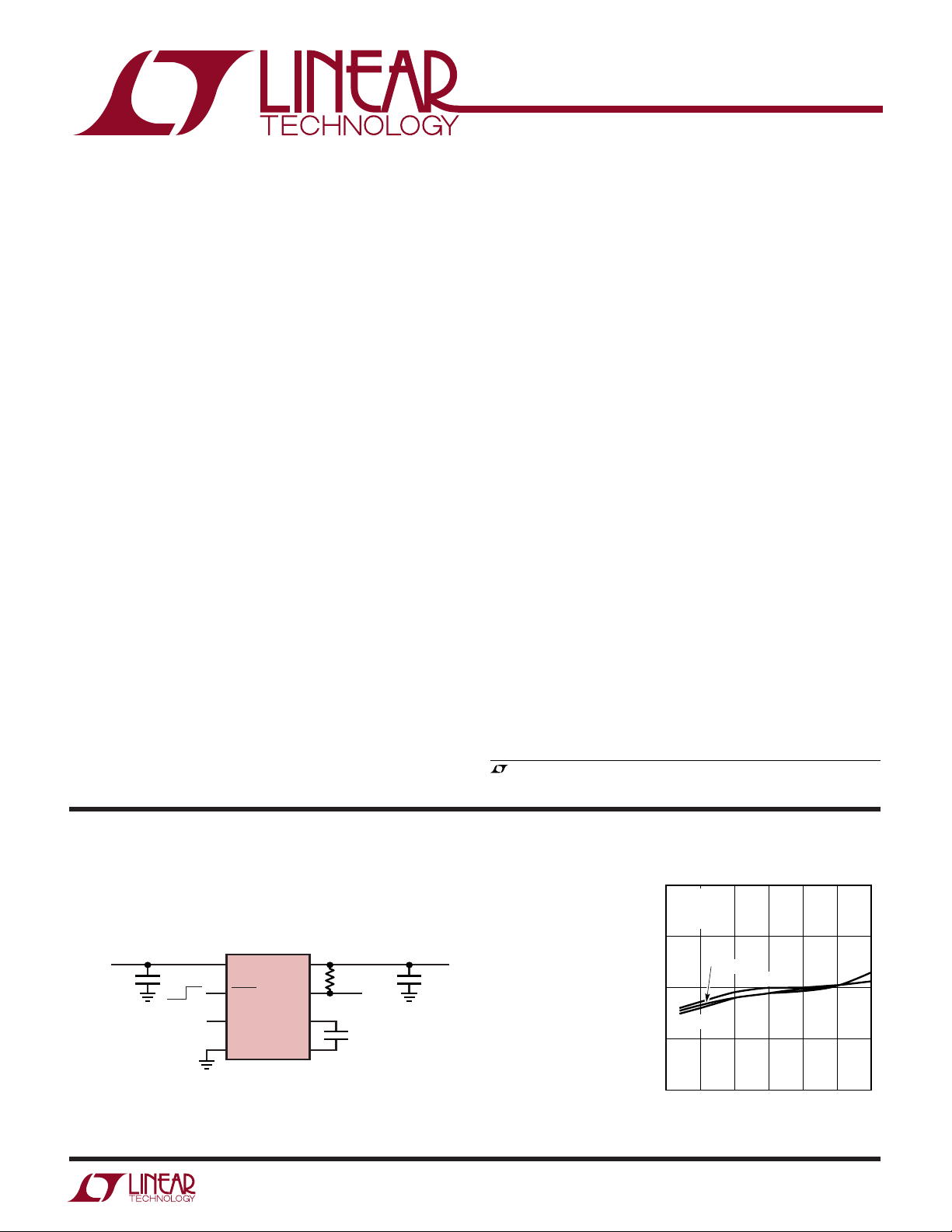
INPUT VOLTAGE (V)
2.5
4.8
OUTPUT VOLTAGE (V)
4.9
5.0
5.1
5.2
3.0 3.5 4.0 4.5
1751 TA02
5.0 5.5
I
OUT
= 50mA
C
FLY
= 1µF
C
OUT
= 10µF
TA = 25°C
T
A
= –40°C
TA = 85°C
■
5V Output Current: 100mA (VIN ≥ 3V)
■
3.3V Output Current: 80mA (VIN ≥ 2.5V)
■
Ultralow Power: 20µA Quiescent Current
■
Regulated Output Voltage: 3.3V ±4%, 5V ±4%, ADJ
■
No Inductors
■
Short-Circuit/Thermal Protection
■
VIN Range: 2V to 5.5V
■
800kHz Switching Frequency
■
Very Low Shutdown Current: <2µA
■
Shutdown Disconnects Load from V
■
PowerGood/Undervoltage Output
■
Adjustable Soft-Start Time
■
Available in an 8-Pin MSOP Package
IN
U
APPLICATIO S
■
Li-Ion Battery Backup Supplies
■
Local 3V and 5V Conversion
■
Smart Card Readers
■
PCMCIA Local 5V Supplies
■
White LED Backlighting
LTC1751/LTC1751-3.3/LTC1751-5
Micropower, Regulated
Charge Pump
DC/DC Converters
U
DESCRIPTIO
The LTC®1751 family are micropower charge pump DC/
DC converters that produce a regulated output voltage at
up to 100mA. The input voltage range is 2V to 5.5V.
Extremely low operating current (20µA typical with no
load) and low external parts count (one flying capacitor
and two small bypass capacitors at VIN and V
them ideally suited for small, battery-powered applications.
The LTC1751 family operate as Burst ModeTM switched
capacitor voltage doublers to achieve ultralow quiescent
current. They have thermal shutdown capability and can
survive a continuous short circuit from V
OUT
PGOOD pin on the LTC1751-3.3 and LTC1751-5 indicates
when the output voltage has reached its final value and if
the output has an undervoltage fault condition. The FB pin
of the adjustable LTC1751 can be used to program the
desired output voltage or current. An optional soft-start
capacitor may be used at the SS pin to prevent excessive
inrush current during start-up.
The LTC1751 family is available in an 8-pin MSOP
package.
, LTC and LT are registered trademarks of Linear Technology Corporation.
Burst Mode is a trademark of Linear Technology Corporation.
) make
OUT
to GND. The
TYPICAL APPLICATIO
V
2.7V
TO 5.5V
IN
C2
10µF
OFF ON
U
Regulated 5V Output from a 2.7V to 5.5V Input
3
V
IN
7
SHDN
LTC1751-5
8
SS
4
GND
C
= MURATA GRM39X5R105K6.3AJ
FLY
C1, C2 = MURATA GRM40X5R106K6.3AJ
V
OUT
PGOOD
1751 TA01
2
R1
100k
1
6
+
C
5
–
C
C
1µF
PGOOD
FLY
C1
10µF
V
5V ±4%
I
OUT
I
OUT
OUT
≤ 100mA, VIN ≥ 3V
≤ 50mA, VIN ≥ 2.7V
Output Voltage vs Input Voltage
1
LTC1751/LTC1751-3.3/LTC1751-5
PACKAGE/ORDER I FOR ATIO
UU
W
1
2
3
4
FB/PGOOD*
V
OUT
V
IN
GND
8
7
6
5
SS
SHDN
C
+
C
–
TOP VIEW
MS8 PACKAGE
8-LEAD PLASTIC MSOP
WWWU
ABSOLUTE AXI U RATI GS
(Note 1)
VIN to GND.................................................. –0.3V to 6V
PGOOD, FB, V
SS, SHDN to GND........................ –0.3V to (VIN + 0.3V)
V
Short-Circuit Duration............................. Indefinite
OUT
I
(Note 2)....................................................... 125mA
OUT
Operating Temperature Range (Note 3) .. –40°C to 85°C
Storage Temperature Range ................ –65°C to 150°C
Lead Temperature (Soldering, 10 sec)................. 300°C
to GND ........................... –0.3V to 6V
OUT
ORDER PART
NUMBER
LTC1751EMS8
LTC1751EMS8-3.3
LTC1751EMS8-5
MS8 PART MARKING
T
= 150°C, θJA = 160°C/W
JMAX
*PGOOD ON LTC1751-3.3/LTC1751-5
FB ON LTC1751
LTKL
LTKN
LTKP
Consult factory for parts specified with wider operating temperature ranges.
ELECTRICAL CHARACTERISTICS
temperature range, otherwise specifications are at TA = 25°C. C
SYMBOL PARAMETER CONDITIONS MIN TYP MAX UNITS
LTC1751-3.3
V
IN
V
OUT
I
CC
V
R
η Efficiency VIN = 2V, I
LTC1751-5
V
IN
V
OUT
I
CC
V
R
η Efficiency VIN = 3V, I
LTC1751
V
IN
I
CC
V
FB
I
FB
R
OUT
Input Supply Voltage ● 2 4.4 V
Output Voltage 2V ≤ VIN ≤ 4.4V, I
2.5V ≤ VIN ≤ 4.4V, I
Operating Supply Current 2V ≤ VIN ≤ 4.4V, I
Output Ripple VIN = 2.5V, I
Input Supply Voltage ● 2.7 5.5 V
Output Voltage 2.7V ≤ VIN ≤ 5.5V, I
Operating Supply Current 2.7V ≤ VIN ≤ 5.5V, I
Output Ripple VIN = 3V, I
Input Supply Voltage ● 2 5.5 V
Operating Supply Current 2V ≤ VIN ≤ 5.5V, I
FB Regulation Voltage 2V ≤ VIN ≤ 5.5V, I
FB Input Current VFB = 1.3V ● –50 50 nA
Open-Loop Charge Pump Strength VIN = 2V, V
3V ≤ V
= 2.7V, V
V
IN
The ● denotes specifications which apply over the full specified
= 1µF, CIN = 10µF, C
FLY
≤ 40mA ● 3.17 3.3 3.43 V
OUT
≤ 80mA ● 3.17 3.3 3.43 V
OUT
= 0mA, SHDN = V
OUT
= 40mA 68 mV
OUT
= 40mA 80 %
OUT
≤ 50mA ● 4.8 5 5.2 V
≤ 5.5V, I
IN
OUT
OUT
OUT
≤ 100mA ● 4.8 5 5.2 V
OUT
= 0mA, SHDN = V
OUT
= 50mA 75 mV
= 50mA 82 %
= 0mA, SHDN = V
OUT
≤ 20mA ● 1.157 1.205 1.253 V
OUT
= 3.3V (Note 5) ● 8.5 20 Ω
OUT
= 5V (Note 5) ● 6.0 12 Ω
OUT
IN
IN
= 10µF unless otherwise noted.
OUT
● 18 40 µA
IN
(Note 4 ) ● 16 40 µA
● 20 50 µA
P-P
P-P
2
LTC1751/LTC1751-3.3/LTC1751-5
ELECTRICAL CHARACTERISTICS
temperature range, otherwise specifications are at TA = 25°C. C
The ● denotes specifications which apply over the full specified
= 1µF, CIN = 10µF, C
FLY
= 10µF unless otherwise noted.
OUT
SYMBOL PARAMETER CONDITIONS MIN TYP MAX UNITS
LTC1751-3.3/LTC1751-5
UVL PGOOD Undervoltage Low Threshold Relative to Regulated V
UVH PGOOD Undervoltage High Threshold Relative to Regulated V
V
OL
I
OH
PGOOD Low Output Voltage I
PGOOD High Output Leakage V
= –500µA ● 0.4 V
PGOOD
= 5.5V ● 1 µA
PGOOD
(Note 6) ● –11 –7 –3 %
OUT
(Note 6) ● –8 –4.5 –2 %
OUT
LTC1751/LTC1751-3.3/LTC1751-5
I
SHDN
V
IH
V
IL
I
IH
I
IL
t
r
f
OSC
Note 1: Absolute Maximum Ratings are those values beyond which the life
of a device may be impaired.
Note 2: Based on long term current density limitations.
Note 3: The LTC1751EMS8-X is guaranteed to meet performance
Shutdown Supply Current VIN ≤ 3.6V, V
3.6V < V
= 0V, V
OUT
, V
= 0V, V
IN
OUT
= 0V ● 0.01 2 µA
SHDN
= 0V ● 5 µA
SHDN
SHDN Input Threshold (High) ● 1.5 V
SHDN Input Threshold (Low) ● 0.3 V
SHDN Input Current (High) SHDN = V
IN
● –1 1 µA
SHDN Input Current (Low) SHDN = 0V ● –1 1 µA
V
Rise Time VIN = 3V, I
OUT
= 0mA, 10% to 90% (Note 6) 0.6ms/nF • C
OUT
SS
sec
Switching Frequency Oscillator Free Running 800 kHz
Note 4: The no load input current will be approximately I
plus twice the
CC
standing current in the resistive output divider.
Note 5: R
≡ (2VIN – V
OUT
OUT
)/I
OUT
.
Note 6: See Figure 2.
specifications from 0°C to 70°C. Specifications over the –40°C to 85°C
operating temperature range are assured by design, characterization and
correlation with statistical process controls.
UW
TYPICAL PERFOR A CE CHARACTERISTICS
(LTC1751-3.3)
Output Voltage vs Load Current
3.40
TA = 25°C
= 1µF
C
FLY
3.35
3.30
VIN = 2V
OUTPUT VOLTAGE (V)
3.25
3.20
0
25 50 75 100
LOAD CURRENT (mA)
VIN = 2.5V
125 150
1751 G01
Output Voltage vs Input Voltage
3.40
I
= 40mA
OUT
= 1µF
C
FLY
C
= 10µF
OUT
3.35
3.30
OUTPUT VOLTAGE (V)
3.25
3.20
2.0
2.5
INPUT VOLTAGE (V)
3.0
TA = 25°C
3.5
TA = –40°C
TA = 85°C
4.0
1751 G02
4.5
No Load Supply Current
vs Input Voltage
40
I
= 0mA
OUT
= 1µF
C
FLY
V
= V
SHDN
30
20
SUPPLY CURRENT (µA)
10
0
2.0
IN
2.5
3.0
INPUT VOLTAGE (V)
TA = 85°C
TA = 25°C
TA = –40°C
3.5
4.0
4.5
1751 G03
3
LTC1751/LTC1751-3.3/LTC1751-5
UW
TYPICAL PERFOR A CE CHARACTERISTICS
(LTC1751-3.3)
Power Efficiency vs Load Current
100
TA = 25°C
90
= 1µF
C
FLY
= 10µF
C
OUT
80
70
60
50
40
EFFICIENCY (%)
30
20
10
0
0.001
VIN = 2V
VIN = 2.75V
VIN = 3.3V
VIN = 4.4V
0.01 0.1 1 10 100
LOAD CURRENT (mA)
1751 G04
250
200
150
OUTPUT CURRENT (mA)
100
50
2.0
Short-Circuit Output Current
vs Input Voltage
TA = 25°C
C
= 1µF
FLY
2.5
INPUT VOLTAGE (V)
3.0
3.5
4.0
4.5
1751 G05
Start-Up
SHDN
2V/DIV
PGOOD
5V/DIV
V
OUT
1V/DIV
CSS = 10nF 2ms/DIV 1751 G06
(LTC1751-5)
Output Voltage vs Output Current
5.2
TA = 25°C
C
5.1
5.0
OUTPUT VOLTAGE (V)
4.9
FLY
= 1µF
AC COUPLED
V
IN
VIN = 2.7V
Output Ripple
V
OUT
50mV/DIV
VIN = 2.5V 5µs/DIV 1751 G07
I
= 80mA
OUT
C
= 10µF
OUT
= 3V
40mA/DIV
AC COUPLED
50mV/DIV
No Load Supply Current
vs Input Voltage
40
C
= 1µF
FLY
= 0
I
OUT
= V
V
SHDN
30
20
SUPPLY CURRENT (µA)
10
IN
TA = –40°C
Load Transient Response
I
OUT
V
OUT
VIN = 2.5V 50µs/DIV 1751 G08
TA = 85°C
TA = 25°C
4
4.8
0
50
100
OUTPUT CURRENT (mA)
150
200
1751 G09
0
2.5
3.0 3.5 4.0 4.5
INPUT VOLTAGE (V)
5.0 5.5
1751 G10

LTC1751/LTC1751-3.3/LTC1751-5
UW
TYPICAL PERFOR A CE CHARACTERISTICS
(LTC1751-5)
Power Efficiency vs Load Current
100
TA = 25°C
= 1µF
C
90
FLY
C
= 10µF
OUT
80
70
60
50
40
EFFICIENCY (%)
30
20
10
0
0.001
VIN = 2.7V
VIN = 4.1V
VIN = 5.5V
0.01 0.1 1 10 100
LOAD CURRENT (mA)
1751 G11
250
200
150
OUTPUT CURRENT (mA)
100
50
Short-Circuit Output Current
vs Input Voltage
TA = 25°C
= 1µF
C
FLY
2.0
2.5 3.0 3.5 4.0
INPUT VOLTAGE (V)
4.5 5.0 5.5
1751 G12
Start-Up
SHDN
2V/DIV
PGOOD
5V/DIV
V
OUT
2V/DIV
CSS = 10nF 2ms/DIV 1751 G13
U
UU
AC COUPLED
Output Ripple
V
OUT
50mV/DIV
VIN = 3V 5µs/DIV 1751 G14
I
= 100mA
OUT
C
= 10µF
OUT
PI FU CTIO S
PGOOD (Pin 1) (LTC1751-3.3/LTC1751-5): Output Voltage Status Indicator. On start-up, this open-drain pin remains low until the output voltage, V
(typ) of its final value. Once V
high-Z. If, due to a fault condition, V
is valid, PGOOD becomes
OUT
OUT
its correct regulation level, PGOOD pulls low. PGOOD may
be pulled up through an external resistor to any appropriate reference level.
FB (Pin 1) (LTC1751): The voltage on this pin is compared
to the internal reference voltage (1.205V) by the error
comparator to keep the output in regulation. An external
resistor divider is required between V
gram the output voltage.
V
(Pin 2): Regulated Output Voltage. For best perfor-
OUT
mance, V
should be bypassed with a 6.8µF (min) low
OUT
ESR capacitor as close to the pin as possible .
, is within 4.5%
OUT
falls 7% (typ) below
and FB to pro-
OUT
Load Transient Response
I
OUT
50mA/DIV
V
OUT
AC COUPLED
50mV/DIV
VIN = 3V 50µs/DIV 1751 G15
VIN (Pin 3): Input Supply Voltage. VIN should be bypassed
with a 6.8µF (min) low ESR capacitor.
GND (Pin 4): Ground. Should be tied to a ground plane for
best performance.
C– (Pin 5): Flying Capacitor Negative Terminal.
C+ (PIN 6): Flying Capacitor Positive Terminal.
SHDN (Pin 7): Active Low Shutdown Input. A low on
SHDN disables the device. SHDN must not be allowed to
float.
SS (Pin 8): Soft-Start Programming Pin. A capacitor on SS
programs the start-up time of the charge pump so that
large start-up input current is eliminated.
5

LTC1751/LTC1751-3.3/LTC1751-5
W
SI PLIFIEDWBLOCK DIAGRA S
LTC1751-3.3/LTC1751-5
PGOOD
READY
1
+
+
–
–
–
+
–
+
UNDERV
V
2 7
OUT
V
3
IN
GND
4
+
–
COMP1
CHARGE PUMP
V
REF
CONTROL
2µA
8
6
5
SS
SHDN
C
C
1751 BD1
+
–
LTC1751
FB
1
V
2 7
OUT
V
3
IN
GND
4
+
COMP1
–
CONTROL
CHARGE PUMP
2µA
SS
8
V
REF
SHDN
+
C
6
–
5
C
6
1751 BD2

WUUU
APPLICATIO S I FOR ATIO
LTC1751/LTC1751-3.3/LTC1751-5
Operation (Refer to Simplified Block Diagrams)
The LTC1751 family uses a switched capacitor charge
pump to boost VIN to a regulated output voltage. Regulation is achieved by sensing the output voltage through a
resistor divider and enabling the charge pump when the
divided output drops below the lower trip point of COMP1.
When the charge pump is enabled, a 2-phase
nonoverlapping clock activates the charge pump switches.
The flying capacitor is charged to VIN on phase 1 of the
clock. On phase 2 of the clock, it is stacked in series with
VIN and connected to V
. This sequence of charging and
OUT
discharging the flying capacitor continues at the clock
frequency until the divided output voltage reaches the
upper trip point of COMP1. Once this happens the charge
pump is disabled. When the charge pump is disabled the
device typically draws less than 20µA from VIN thus
providing high efficiency under low load conditions.
In shutdown mode all circuitry is turned off and the
LTC1751 draws only leakage current from the VIN supply.
Furthermore, V
is disconnected from VIN. The SHDN
OUT
pin is a CMOS input with a threshold voltage of approximately 0.8V. The LTC1751 is in shutdown when a logic low
is applied to the SHDN pin. The quiescent supply current
of the LTC1751 will be slightly higher if the SHDN pin is
driven high with a voltage that is below VIN than if it is
driven all the way to VIN. Since the SHDN pin is a high
impedance CMOS input it should never be allowed to float.
To ensure that its state is defined it must always be driven
with a valid logic level.
Power Efficiency
The efficiency (η) of the LTC1751 family is similar to that
of a linear regulator with an effective input voltage of twice
the actual input voltage. This occurs because the input
current for a voltage doubling charge pump is approximately twice the output current. In an ideal regulated
doubler the power efficiency would be given by:
P
OUT
η= = =
P
VI
OUT OUT
VIVV
IN
IN OUT
•
•2 2
OUT
IN
At moderate to high output power, the switching losses
and quiescent current of the LTC1751 are negligible and
the expression is valid. For example, an LTC1751-5 with
VIN = 3V, I
= 50mA and V
OUT
regulating to 5V, has a
OUT
measured efficiency of 82% which is in close agreement
with the theoretical 83.3% calculation. The LTC1751 product family continues to maintain good efficiency even at
fairly light loads because of its inherently low power
design.
Short-Circuit/Thermal Protection
During short-circuit conditions, the LTC1751 will draw
between 200mA and 400mA from VIN causing a rise in the
junction temperature. On-chip thermal shutdown circuitry
disables the charge pump once the junction temperature
exceeds approximately 160°C and re-enables the charge
pump once the junction temperature drops back to approximately 150°C. The device will cycle in and out of
thermal shutdown indefinitely without latchup or damage
until the short circuit on V
VIN, V
Capacitor Selection
OUT
is removed.
OUT
The style and value of capacitors used with the LTC1751
family determine several important parameters such as
output ripple, charge pump strength and minimum
start-up time.
To reduce noise and ripple, it is recommended that low
ESR (<0.1Ω) capacitors be used for both CIN and C
OUT
.
These capacitors should be either ceramic or tantalum and
should be 6.8µF or greater. Aluminum capacitors are not
recommended because of their high ESR. If the source
impedance to VIN is very low, up to several megahertz, C
IN
may not be needed. Alternatively, a somewhat smaller
value of input capacitor may be adequate, but will not be
as effective in preventing ripple on the VIN pin.
The value of C
Increasing the size of C
controls the amount of output ripple.
OUT
to 10µF or greater will reduce
OUT
the output ripple at the expense of higher minimum turn on
time and higher start-up current. See the section Output
Ripple.
7

LTC1751/LTC1751-3.3/LTC1751-5
WUUU
APPLICATIO S I FOR ATIO
Flying Capacitor Selection
Warning: A polarized capacitor such as tantalum or
aluminum should never be used for the flying capacitor
since its voltage can reverse upon start-up of the LTC1751.
Low ESR ceramic capacitors should always be used for
the flying capacitor.
The flying capacitor controls the strength of the charge
pump. In order to achieve the rated output current, it is
necessary to have at least 0.6µF of capacitance for the
flying capacitor. Capacitors of different materials lose their
capacitance with higher temperature and voltage at different rates. For example, a ceramic capacitor made of X7R
material will retain most of its capacitance from –40°C to
85°C, whereas, a Z5U or Y5V style capacitor will lose
considerable capacitance over that range. Z5U and Y5V
capacitors may also have a very strong voltage coefficient
causing them to lose 50% or more of their capacitance
when the rated voltage is applied. The capacitor
manufacturer’s data sheet should be consulted to determine what value of capacitor is needed to ensure 0.6µF at
all temperatures and voltages.
Generally an X7R ceramic capacitor is recommended for
the flying capacitor with a minimum value of 1µF. For very
low load applications, it may be reduced to 0.01µF-0.68µF.
A smaller flying capacitor delivers less charge per clock
cycle to the output capacitor resulting in lower output
ripple. The output ripple is reduced at the expense of
maximum output current and efficiency.
The theoretical minimum output resistance of a voltage
doubling charge pump is given by:
–
21
VV
IN OUT
R
OUT MIN
Where f if the switching frequency and C is the value of the
flying capacitor. (Using units of MHz and µF is convenient
since they cancel each other.) Note that the charge pump
will typically be weaker than the theoretical limit due to
additional switch resistance. However, for light load applications, the above expression can be used as a guideline
in determining a starting capacitor value.
≡=
()
IfC
OUT
Below is a list of ceramic capacitor manufacturers and
how to contact them:
AVX www.avxcorp.com
Kemet www.kemet.com
Murata www.murata.com
Taiyo Yuden www.t-yuden.com
Vishay www.vishay.com
Output Ripple
Low frequency
hysteresis in the sense comparator and propagation
delays in the charge pump control circuits. The amplitude
and frequency of this ripple are heavily dependent on the
load current, the input voltage and the output capacitor
size. For large VIN the ripple voltage can become substantial because the increased strength of the charge pump
causes fast edges that may outpace the regulation circuitry. In some cases, rather than bursting, a single
output cycle may be enough to boost the output voltage
into or possibly beyond regulation. In these cases the
average output voltage will climb slightly. For large input
voltages a larger output capacitor will ensure that bursting always occurs, thus mitigating possible DC problems.
Generally the regulation ripple has a sawtooth shape
associated with it.
A high frequency ripple component may also be present
on the output capacitor due to the charge transfer action
of the charge pump. In this case, the output can display a
voltage pulse during the output-charging phase. This
pulse results from the product of the charging current and
the ESR of the output capacitor. It is proportional to the
input voltage, the value of the flying capacitor and the ESR
of the output capacitor.
For example, typical combined output ripple for an
LTC1751-5 with VIN = 3V under maximum load is
75mV
output capacitor and/or larger output current load will
result in higher ripple due to higher output voltage slew
rates.
with a low ESR 10µF output capacitor. A smaller
P-P
regulation mode
ripple exists due to the
8

WUUU
APPLICATIO S I FOR ATIO
LTC1751/LTC1751-3.3/LTC1751-5
There are several ways to reduce output voltage ripple.
For applications requiring VIN to exceed 3.3V or for
applications requiring <100mV of peak-to-peak ripple, a
larger C
capacitor (22µF or greater) is recommended.
OUT
A larger capacitor will reduce both the low and high
frequency ripple due to the lower charging and discharging slew rates as well as the lower ESR typically found
with higher value (larger case size) capacitors. A low ESR
ceramic output capacitor will minimize the high frequency ripple, but will not reduce the low frequency
ripple unless a high capacitance value is used. An R-C
filter may also be used to reduce high frequency voltages
spikes (see Figure 1).
V
OUT
LTC1751-X
Figure 1. Output Ripple Reduction Technique
1Ω
+
10µF
TANT
+
10µF
TANT
V
5V
1751 F01
OUT
Note that when using a larger output capacitor the minimum turn-on time of the device will increase.
Soft-Start
various parameters such as temperature, output loading,
charge pump and flying capacitor values and input
voltage.
PGOOD and Undervoltage Detection
The PGOOD pin on the LTC1751-3.3/LTC1751-5 performs
two functions. On start-up, it indicates when the output
has reached its final regulation level. After start-up, it
indicates when a fault condition, such as excessive loading, has pulled the output out of regulation.
Once the LTC1751-3.3/LTC1751-5 are enabled via the
SHDN pin, V
ramps to its final regulation value slowly
OUT
by following the SS pin. The PGOOD pin switches from low
impedance to high impedance after V
regulation value. If V
is subsequently pulled below its
OUT
reaches its
OUT
correct regulation level, the PGOOD pin pulls low again
indicating that a fault exists. Alternatively, if there is a short
circuit on V
preventing it from ever reaching its correct
OUT
regulation level, the PGOOD pin will remain low. The lower
fault threshold, UVL, is preprogrammed to recognize
errors of –7% below nominal V
. The upper fault
OUT
threshold, UVH, is preprogrammed at – 4.5% below nominal. Figure 2 shows an example of the PGOOD pin with a
normal start-up followed by an undervoltage fault.
The LTC1751 family has built-in soft-start circuitry to
prevent excessive current flow at VIN during start-up. The
soft-start time is programmed by the value of the capacitor
at the SS pin. Typically a 2µA current is forced out of SS
causing a ramp voltage on the SS pin. The regulation loop
follows this ramp voltage until the output reaches the
correct regulation level. SS is automatically pulled to
ground whenever SHDN is low. The typical rise time is
given by the expression:
tr = 0.6ms/nF • C
SS
For example, with a 4.7nF capacitor the 10% to 90% rise
time will be approximately 2.8ms. If the output charge
storage capacitor is 10µF, then the average output current
for an LTC1751-5 will be 4V/2.8ms • 10µF or 14mA, giving
28mA at the VIN pin.
The soft-start feature is optional. If there is no capacitor
on SS, the output voltage of the LTC1751 will ramp up as
quickly as possible. The start-up time will depend on
Using an external pull-up resistor, the PGOOD pin can be
pulled high from any available voltage supply, including
the LTC1751-3.3/LTC1751-5 V
OUT
pin.
If PGOOD is not used it may be connected to GND.
SHDN
PGOOD
t
90%
V
OUT
10%
Figure 2. PGOOD During Start-Up and Undervoltage
r
TIME
UVL
UVH
17515 F02
9

LTC1751/LTC1751-3.3/LTC1751-5
WUUU
APPLICATIO S I FOR ATIO
Programming the LTC1751 Output Voltage (FB Pin)
While the LTC1751-3.3/LTC1751-5 versions have internal
resistive dividers to program the output voltage, the
programmable LTC1751 may be set to an arbitrary voltage
via an external resistive divider. Since it employs a voltage
doubling charge pump, it is not possible to achieve output
voltages greater than twice the available input voltage.
Figure 3 shows the required voltage divider connection.
The voltage divider ratio is given by the expression:
R
R
V
1
OUT
.
2 1 205
1=
–
V
V
GND
OUT
FB
1751 F03
2
R1
1
R2
4
V
OUT
1.205V 1 +
C
OUT
R1
()
R2
Figure 3. Programming the Adjustable LTC1751
The sum of the voltage divider resistors can be made large
to keep the quiescent current to a minimum. Any standing
current in the output divider (given by 1.205V/R2) will be
reflected by a factor of 2 in the input current. Typical values
for total voltage divider resistance can range from several
kΩs up to 1MΩ.
Maximum Available Output Current
For the adjustable LTC1751, the maximum available output current and voltage can be calculated from the effective open-loop output resistance, R
output voltage, 2V
IN(MIN)
.
, and effective
OUT
From Figure 4 the available current is given by:
VV
2–
=
IN OUT
R
OUT
I
OUT
Typical R
values as a function of input voltage are
OUT
shown in Figure 5.
10
TA = 25°C
= 1µF
C
FLY
8
I
= 100mA
6
4
OUTPUT RESISTANCE (Ω)
2
0
2.5
2.0
Figure 5. Typical R
OUT
I
= 50mA
OUT
3.5
3.0
INPUT VOLTAGE (V)
vs Input Voltage
OUT
4.0
4.5
1751 F05
Layout Considerations
Due to high switching frequency and high transient currents produced by the LTC1751 product family, careful
board layout is necessary. A true ground plane and short
connections to all capacitors will improve performance and
ensure proper regulation under all conditions. Figure 6
shows the recommended layout configuration.
Thermal Management
For higher input voltages and maximum output current,
there can be substantial power dissipation in the
LTC1751. If the junction temperature increases above
approximately 160°C, the thermal shutdown circuitry
will automatically deactivate the output. To reduce the
maximum junction temperature, a good thermal connection to the PC board is recommended. Connecting the
GND pin (Pin 4) to a ground plane, and maintaining a
solid ground plane under the device on two layers of the
PC board, will reduce the thermal resistance of the
package and PC board system considerably.
V
IN
10
R
OUT
+
2V
IN
–
+
V
OUT
–
1751 F04
Figure 4. Equivalent Open-Loop Circuit
V
OUT
GND
Figure 6. Recommended Layout
SHDN
17515 F03

TYPICAL APPLICATIO S
LTC1751/LTC1751-3.3/LTC1751-5
U
USB Port to Regulated 5V Power Supply with Soft-Start
1µF
65
+
–
C
1nF
3
7
8
C
V
IN
LTC1751-5
SHDN
SS
GND
V
OUT
PGOOD
4
2
1
10µF10µF
1751 TA04
V
100k
PGOOD
OUT
= 5V
1Ω
Boosted Constant Current Source
1µF
–
C
3
OFF
V
IN
ON
V
IN
LTC1751
7
SHDN
8
SS
GND
4
2-Cell NiCd or NiMH to 3.3V with Low Standby Current
1µF
65
+
–
C
C
3
V
1nF
7
SHDN
8
SS
IN
LTC1751-3.3
GND
2-CELL
NiCd OR
65
+
C
2
V
OUT
10µF10µF
1
FB
NiMH
LOAD
+
+
OFF
ON
1.205V
I
=
L
R
X
V
≤ 2 V
OUT
IN
R
X
1751 TA07
V
OUT
PGOOD
4
2
1
10µF10µF
1751 TA06
3.3V
40mA
100k
PGOOD
Low Power Battery Backup with Auto Switchover and No Reverse Current
Si4435DY
1µF
65
+
–
C
3
8
BAT54C
4
3
6
5
HYST
C
V
IN
LTC1751-5
SS
GND
–
+
V
OUT
PGOOD
SHDN
4
7
LTC1540
2
2
10µF10µF10µF
1
7
8
1
V
= 5V
OUT
≤ 100mA
I
OUT
100k
HIGH = BACKUP MODE
1751 TA05
IN4148
1.43M
475k
75k
3-CELL
NiCd
BATTERY
+
+
+
330pF
10k
1M
V
= 5V
IN
Information furnished by Linear Technology Corporation is believed to be accurate and reliable.
However, no responsibility is assumed for its use. Linear Technology Corporation makes no representation that the interconnection of its circuits as described herein will not infringe on existing patent rights.
11

LTC1751/LTC1751-3.3/LTC1751-5
U
TYPICAL APPLICATIO
Current Mode White or Blue LED Driver with PWM Brightness Control
C4
1µF
65
+
–
C
3
7
8
C
V
IN
SHDN
SS
C3
680pF
LTC1751
V
GND
OUT
FB
Li-Ion
BATTERY
3V TO 4.5V
10µF
C1
V
SHDN
17ms
t
U
PACKAGE DESCRIPTIO
0.007
(0.18)
0.021 ± 0.006
(0.53 ± 0.015)
* DIMENSION DOES NOT INCLUDE MOLD FLASH, PROTRUSIONS OR GATE BURRS. MOLD FLASH,
PROTRUSIONS OR GATE BURRS SHALL NOT EXCEED 0.006" (0.152mm) PER SIDE
** DIMENSION DOES NOT INCLUDE INTERLEAD FLASH OR PROTRUSIONS.
INTERLEAD FLASH OR PROTRUSIONS SHALL NOT EXCEED 0.006" (0.152mm) PER SIDE
0° – 6° TYP
SEATING
PLANE
Dimensions in inches (millimeters) unless otherwise noted.
MS8 Package
8-Lead Plastic MSOP
(LTC DWG # 05-08-1660)
0.043
(1.10)
MAX
0.009 – 0.015
(0.22 – 0.38)
0.0256
(0.65)
BSC
2
1
4
C2
10µF
0.034
(0.86)
REF
0.005 ± 0.002
(0.13 ± 0.05)
MSOP (MS8) 1100
82Ω
UP TO 6 LEDS
82Ω
0.118 ± 0.004*
(3.00 ± 0.102)
0.193 ± 0.006
(4.90 ± 0.15)
82Ω 82Ω 82Ω 82Ω
1751 TA03
8
7
6
5
0.118 ± 0.004**
(3.00 ± 0.102)
12
4
3
RELATED PARTS
PART NUMBER DESCRIPTION COMMENTS
LTC1144 Charge Pump Inverter with Shutdown VIN = 2V to 18V, 15V to –15V Supply
LTC1262 12V, 30mA Flash Memory Prog. Supply Regulated 12V ±5% Output, IQ = 500µA
LTC1514/LTC1515 Buck/Boost Charge Pumps with IQ = 60µA 50mA Output at 3V, 3.3V or 5V; 2V to 10V Input
LTC1516 Micropower 5V Charge Pump IQ = 12µA, Up to 50mA Output, VIN = 2V to 5V
LTC1517-5/LTC1517-3.3 Micropower 5V/3.3V Doubler Charge Pumps IQ = 6µA, Up to 20mA Output
LTC1522 Micropower 5V Doubler Charge Pump IQ = 6µA, Up to 20mA Output
LTC1555/LTC1556 SIM Card Interface Step-Up/Step-Down Charge Pump, VIN = 2.7V to 10V
LTC1682 Low Noise Doubler Charge Pump Output Noise = 60µV
LTC1754-5 Micropower 5V Doubler Charge Pump IQ = 13µA, Up to 50mA Output, SOT-23 Package
LTC1755 Smart Card Interface Buck/Boost Charge Pump, IQ = 60µA, VIN = 2.7V to 6V
LTC3200 Constant Frequency Doubler Charge Pump Low Noise, 5V Output or Adjustable
Linear Technology Corporation
12
1630 McCarthy Blvd., Milpitas, CA 95035-7417
(408) 432-1900 ● FAX: (408) 434-0507
●
www.linear-tech.com
, 2.5V to 5.5V Output
RMS
LINEAR TECHNOLOGY CORPORATION 2000
1751f LT/TP 0401 4K • PRINTED IN USA
 Loading...