

Final Electrical Specifications
查询LT1745供应商
LTC1745
Low Noise,12-Bit, 25Msps ADC
FEATURES
■
Sample Rate: 25Msps
■
72.5dB SNR and 96dB SFDR (3.2V Range)
■
71dB SNR and 96dB SFDR (2V Range)
■
No Missing Codes
■
Single 5V Supply
■
Low Power Dissipation: 380mW
■
Selectable Input Ranges: ±1V or ±1.6V
■
240MHz Full Power Bandwidth S/H
■
Output Enable
■
Two’s Complement or Offset Binary Outputs
■
Out-of-Range Indicator
■
Data Ready Output Clock
■
48-Pin TSSOP Package
■
50Msps Pin-for-Pin Upgrade (LTC1743)
■
14-Bit Plug Compatible Upgrade (LTC1746)
U
APPLICATIO S
■
Telecommunications
■
Medical Imaging
■
Receivers
■
Cellular Base Stations
■
Spectrum Analysis
■
Imaging Systems
, LTC and LT are registered trademarks of Linear Technology Corporation.
U
January 2003
DESCRIPTION
The LTC®1745 is a 25Msps, sampling 12-bit A/D converter designed for digitizing high frequency, wide dynamic range signals. Pin selectable input ranges of ±1V
and ±1.6V along with a resistor programmable mode
allow the LTC1745’s input range to be optimized for a wide
variety of applications.
The LTC1745 is perfect for demanding communications
applications with AC performance that includes 72.5dB
SNR and 96dB spurious free dynamic range. Ultralow jitter
of 0.3ps
to 70MHz with excellent noise performance. DC specs
include ±1LSB INL and ±0.75LSB DNL over temperature.
The digital interface is compatible with 5V, 3V and 2V logic
systems. The ENC and ENC inputs may be driven differentially from PECL, GTL and other low swing logic families or
from single-ended TTL or CMOS. The low noise, high gain
ENC and ENC inputs may also be driven by a sinusoidal
signal without degrading performance. A separate output
power supply can be operated from 0.5V to 5V, making it
easy to connect directly to any low voltage DSPs or FIFOs.
The TSSOP package with a flow-through pinout simplifies
the board layout.
allows undersampling of IF frequencies of up
RMS
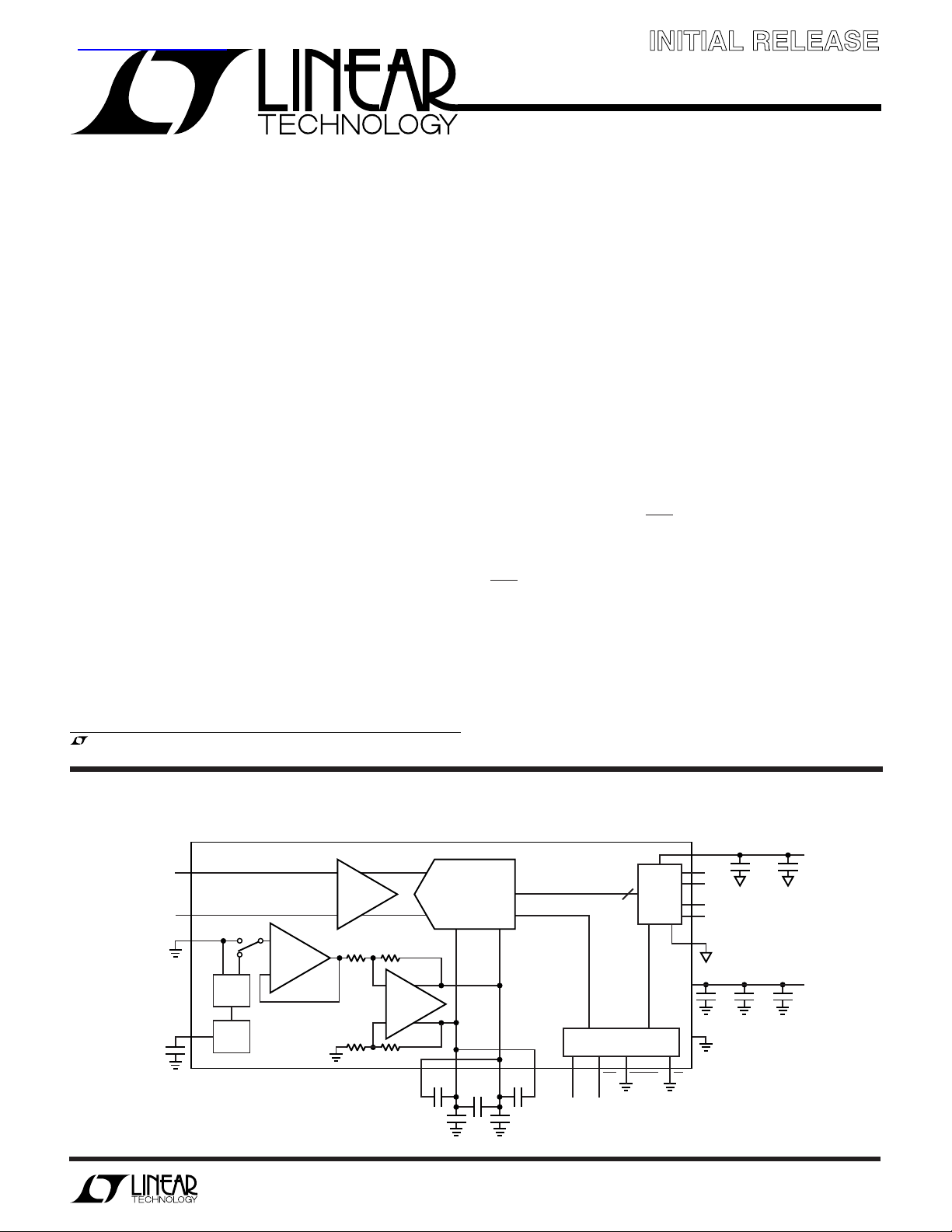
BLOCK DIAGRA
+
A
IN
±1V
DIFFERENTIAL
ANALOG INPUT
4.7µF
A
SENSE
V
–
IN
CM
2.35V
RANGE
SELECT
W
25Msps, 12-Bit ADC with a ±1V Differential Input Range
S/H
AMP
BUFFER
DIFF AMP
REF
0.1µF0.1µF
Information furnished by Linear Technology Corporation is believed to be accurate and reliable.
However, no responsibility is assumed for its use. Linear Technology Corporation makes no representation that the interconnection of its circuits as described herein will not infringe on existing patent rights.
12-BIT
PIPELINED ADC
REFHAREFLB
REFLA REFHB
4.7µF
1µF1µF
CONTROL LOGIC
ENC
DIFFERENTIAL
ENCODE INPUT
ENC
12
OUTPUT
LATCHES
OV
DD
OF
D11
•
•
•
D0
CLKOUT
OGND
V
DD
GND
1745 BD
OEMSBINV
0.1µF
1µF 1µF 1µF
0.5V TO 5V
0.1µF
5V
1745i
1
LTC1745
WW
W
U
ABSOLUTE MAXIMUM RATINGS
OVDD = VDD (Notes 1, 2)
Supply Voltage (VDD)............................................. 5.5V
Analog Input Voltage (Note 3) .... –0.3V to (VDD + 0.3V)
Digital Input Voltage (Note 4) ..... –0.3V to (VDD + 0.3V)
Digital Output Voltage................. –0.3V to (VDD + 0.3V)
OGND Voltage...........................................–0.3V to 0.3V
Power Dissipation............................................ 2000mW
Operating Temperature Range
LTC1745C ............................................... 0°C to 70°C
LTC1745I............................................ – 40°C to 85°C
Storage Temperature Range ................. –65°C to 150°C
Lead Temperature (Soldering, 10 sec).................. 300°C
U
W
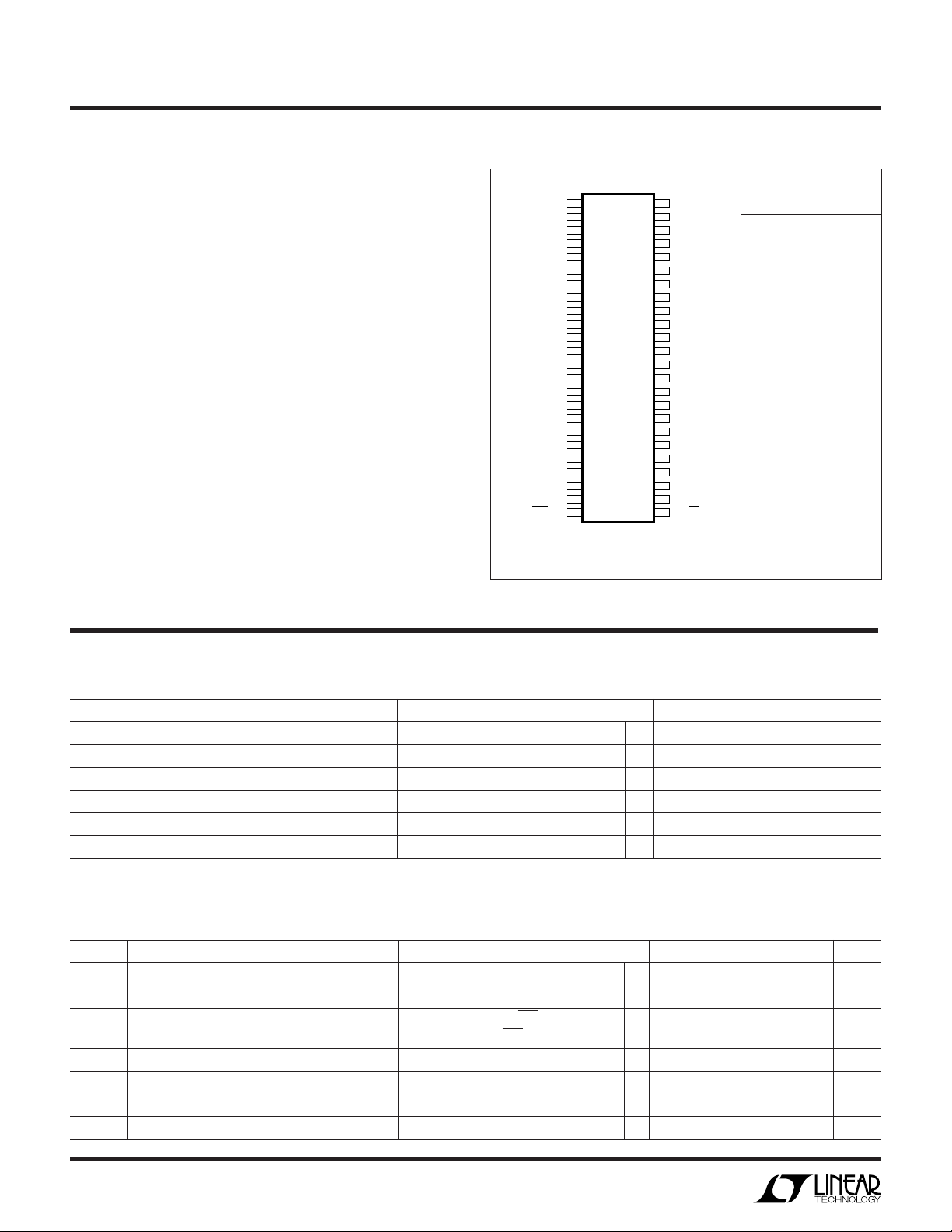
PACKAGE/ORDER INFORMATION
SENSE
V
GND
A
A
GND
V
V
GND
REFLB
REFHA
GND
GND
REFLA
REFHB
GND
V
V
GND
V
GND
MSBINV
ENC
ENC
TOP VIEW
1
2
CM
3
+
4
IN
–
5
IN
6
7
DD
8
DD
9
10
11
12
13
14
15
16
17
DD
18
DD
19
20
DD
21
22
23
24
FW PACKAGE
48-LEAD PLASTIC TSSOP
T
= 150°C, θJA = 35°C/W
JMAX
48
47
46
45
44
43
42
41
40
39
38
37
36
35
34
33
32
31
30
29
28
27
26
25
OF
OGND
D11
D10
D9
OV
DD
D8
D7
D6
D5
OGND
GND
GND
D4
D3
D2
OV
DD
D1
D0
NC
NC
OGND
CLKOUT
OE
ORDER PART
NUMBER
LTC1745CFW
LTC1745IFW
U
Consult LTC Marketing for parts specified with wider operating temperature ranges.
U
CO VERTER CHARACTERISTICS
temperature range, otherwise specifications are at TA = 25°C. (Note 5)
PARAMETER CONDITIONS MIN TYP MAX UNITS
Resolution (No Missing Codes) ● 12 Bits
Integral Linearity Error (Note 6) ● –1 ±0.4 1 LSB
Differential Linearity Error ● –0.75 ±0.2 0.75 LSB
Offset Error (Note 7) ● –30 ±530 mV
Gain Error External Reference (SENSE = 1.6V) ● –2.5 ±1 2.5 %FS
Full-Scale Tempco I
The ● indicates specifications which apply over the full operating
= 0 ±40 ppm/°C
OUT(REF)
UU
A ALOG I PUT
specifications are at TA = 25°C. (Note 5)
SYMBOL PARAMETER CONDITIONS MIN TYP MAX UNITS
V
IN
I
IN
C
IN
t
ACQ
t
AP
t
JITTER
CMRR Analog Input Common Mode Rejection Ratio 1.0V < (A
Analog Input Range (Note 8) 4.75V ≤ VDD ≤ 5.25V ● ±1 to ±1.6 V
Analog Input Leakage Current ● –1 1 µA
Analog Input Capacitance Sample Mode ENC < ENC 8 pF
Sample-and-Hold Acquisition Time ● 15 18 ns
Sample-and-Hold Acquisition Delay Time 0 ns
Sample-and-Hold Acquisition Delay Time Jitter 0.3 ps
The ● indicates specifications which apply over the full operating temperature range, otherwise
Hold Mode ENC > ENC 4 pF
–
+
= A
IN
) < 3.5V 80 dB
IN
RMS
1745i
2
LTC1745
UW
DY A IC ACCURACY
otherwise specifications are at TA = 25°C. AIN = –1dBFS. (Note 5)
SYMBOL PARAMETER CONDITIONS MIN TYP MAX UNITS
SNR Signal-to-Noise Ratio 5MHz Input Signal (2V Range) 71 dB
SFDR Spurious Free Dynamic Range 5MHz Input Signal (2V Range) 96.5 dB
S/(N + D) Signal-to-(Noise + Distortion) Ratio 5MHz Input Signal (2V Range) 71 dB
THD Total Harmonic Distortion 5MHz Input Signal, First 5 Harmonics (2V Range) –95 dB
IMD Intermodulation Distortion f
Sample-and-Hold Bandwidth R
The ● indicates specifications which apply over the full operating temperature range,
5MHz Input Signal (3.2V Range)
30MHz Input Signal (2V Range) 71 dB
30MHz Input Signal (3.2V Range) 72 dB
70MHz Input Signal (2V Range) 70 dB
70MHz Input Signal (3.2V Range) 71.5 dB
5MHz Input Signal (3.2V Range)
30MHz Input Signal (2V Range) 93.5 dB
30MHz Input Signal (3.2V Range) 87.5 dB
70MHz Input Signal (2V Range) 78.5 dB
70MHz Input Signal (3.2V Range) 70.5 dB
5MHz Input Signal (3.2V Range)
30MHz Input Signal (2V Range) 71 dB
30MHz Input Signal (3.2V Range) 72 dB
70MHz Input Signal (2V Range) 69.5 dB
70MHz Input Signal (3.2V Range) 68.5 dB
5MHz Input Signal, First 5 Harmonics (3.2V Range) –93 dB
30MHz Input Signal, First 5 Harmonics (2V Range) –92 dB
30MHz Input Signal, First 5 Harmonics (3.2V Range) –87 dB
70MHz Input Signal, First 5 Harmonics (2V Range) –77.5 dB
70MHz Input Signal, First 5 Harmonics (3.2V Range) –70 dB
= 4MHz, f
IN1
= 4MHz, f
f
IN1
SOURCE
= 5.1MHz (2V Range) 97 dBc
IN2
= 5.1MHz (3.2V Range) 93 dBc
IN2
= 50Ω 240 MHz
● 71 72.5 dB
● 78 96.5 dB
● 71 72.5 dB
UU U
I TER AL REFERE CE CHARACTERISTICS
PARAMETER CONDITIONS MIN TYP MAX UNITS
VCM Output Voltage I
VCM Output Tempco I
VCM Line Regulation 4.75V ≤ VDD ≤ 5.25V 3 mV/V
VCM Output Resistance 1mA ≤ I
= 0 2.29 2.35 2.41 V
OUT
= 0 ±30 ppm/°C
OUT
≤ 1mA 4 Ω
OUT
(Note 5)
1745i
3
LTC1745
UU
DIGITAL I PUTS A D DIGITAL OUTPUTS
operating temperature range, otherwise specifications are at TA = 25°C. (Note 5)
SYMBOL PARAMETER CONDITIONS MIN TYP MAX UNITS
V
IH
V
IL
I
IN
C
IN
V
OH
V
OL
I
OZ
C
OZ
I
SOURCE
I
SINK
High Level Input Voltage VDD = 5.25V ● 2.4 V
Low Level Input Voltage VDD = 4.75V ● 0.8 V
Digital Input Current VIN = 0V to V
Digital Input Capacitance MSBINV and OE Only 1.5 pF
High Level Output Voltage OVDD = 4.75V IO = –10µA 4.74 V
Low Level Output Voltage OVDD = 4.75V IO = 160µA 0.05 V
Hi-Z Output Leakage D11 to D0 V
Hi-Z Output Capacitance D11 to D0 OE = High (Note 8) ● 15 pF
Output Source Current V
Output Sink Current V
OUT
OUT
OUT
DD
= 0V to VDD, OE = High ● ±10 µA
= 0V –50 mA
= 5V 50 mA
The ● indicates specifications which apply over the full
● ±10 µA
IO = –200µA ● 4V
IO = 1.6mA ● 0.1 0.4 V
WU
POWER REQUIRE E TS
range, otherwise specifications are at TA = 25°C. (Note 5)
SYMBOL PARAMETER CONDITIONS MIN TYP MAX UNITS
V
I
DD
P
OV
DD
DIS
DD
Positive Supply Voltage 4.75 5.25 V
Positive Supply Current 2V Range, Full-Scale Input ● 76 91 mA
Power Dissipation 2V Range, Full-Scale Input 380 455 mW
Digital Output Supply Voltage 0.5 V
The ● indicates specifications which apply over the full operating temperature
DD
UW
TI I G CHARACTERISTICS
range, otherwise specifications are at TA = 25°C. (Note 5)
The ● indicates specifications which apply over the full operating temperature
V
SYMBOL PARAMETER CONDITIONS MIN TYP MAX UNITS
f
SAMPLE(MAX)
t
1
t
2
t
3
t
4
t
5
t
6
t
7
t
8
Note 1: Absolute Maximum Ratings are those values beyond which the life
of a device may be impaired.
Note 2: All voltage values are with respect to ground with GND
(unless otherwise noted).
Note 3: When these pin voltages are taken below GND or above V
will be clamped by internal diodes. This product can handle input currents
of greater than 100mA below GND or above V
Note 4: When these pin voltages are taken below GND, they will be
clamped by internal diodes. This product can handle input currents of
>100mA below GND without latchup. These pins are not clamped to V
Maximum Sampling Frequency (Note 9) ● 25 MHz
ENC Low Time (Note 9) ● 19 20 1000 ns
ENC High Time (Note 9) ● 19 20 1000 ns
Aperture Delay of Sample-and-Hold 0 ns
Delay to Data Output CL = 10pF (Note 8) ● 0.5 1.5 5 ns
ENC to CLKOUT Delay (Note 8) ● 013ns
CLKOUT to Data Delay (Note 8) ● 0 0.5 ns
DATA Access Time After OE ↓ CL = 5pF (Note 8) 10 25 ns
BUS Relinquish Time (Note 8) 10 25 ns
without latchup.
DD
DD
, they
DD
Note 5: V
sine wave, input range = ±1.6V differential, unless otherwise specified.
Note 6: Integral nonlinearity is defined as the deviation of a code from a
straight line passing through the actual endpoints of the transfer curve.
The deviation is measured from the center of the quantization band.
Note 7: Bipolar offset is the offset voltage measured from –0.5 LSB
when the output code flickers between 0000 0000 0000 and
1111 1111 1111.
Note 8: Guaranteed by design, not subject to test.
.
Note 9: Recommended operating conditions.
= 5V, f
DD
= 25MHz, differential ENC/ENC = 2V
SAMPLE
P-P
25MHz
1745i
4
UW
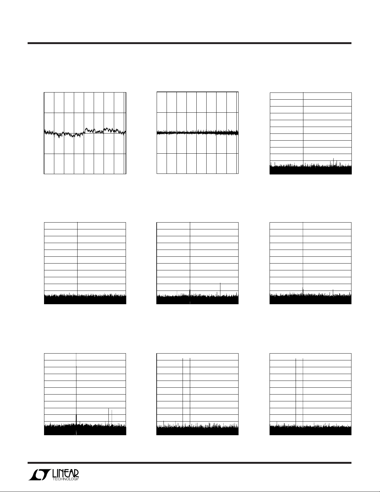
TYPICAL PERFOR A CE CHARACTERISTICS
1.0
0.5
0
INL ERROR (LSB)
–0.5
–1.0
0
1000 2000
CODE
Nonaveraged, 32768 Point FFT,
Input Frequency = 5MHz,
2V Range
0
–10
–20
–30
–40
–50
–60
–70
AMPLITUDE (dB)
–80
–90
–100
–110
–120
0
4
2
FREQUENCY (MHz)
6
Nonaveraged, 32768 Point FFT,
Input Frequency = 70MHz,
2V Range
0
–10
–20
–30
–40
–50
–60
–70
AMPLITUDE (dB)
–80
–90
–100
–110
–120
0
4
2
FREQUENCY (MHz)
6
3000 4000
1745 G01
10
812
1745 G04
10
812
1745 G07
1.0
0.5
0
DNL ERROR (LSB)
–0.5
–1.0
0
1000 2000
CODE
Nonaveraged, 32768 Point FFT,
Input Frequency = 30MHz,
3.2V Range
0
–10
–20
–30
–40
–50
–60
–70
AMPLITUDE (dB)
–80
–90
–100
–110
–120
0
4
2
FREQUENCY (MHz)
6
Nonaveraged, 32768 Point
2-Tone FFT, Input Frequency =
4MHz and 5.1MHz, 3.2V Range
0
–10
–20
–30
–40
–50
–60
–70
AMPLITUDE (dB)
–80
–90
–100
–110
–120
0
4
2
FREQUENCY (MHz)
6
3000 4000
10
812
10
812
1745 G02
1745 G05
1745 G08
LTC1745
Nonaveraged, 32768 Point FFT,
Input Frequency = 5MHz,
3.2V RangeTypical INL Typical DNL
0
–10
–20
–30
–40
–50
–60
–70
AMPLITUDE (dB)
–80
–90
–100
–110
–120
0
Nonaveraged, 32768 Point FFT,
Input Frequency = 30MHz,
2V Range
0
–10
–20
–30
–40
–50
–60
–70
AMPLITUDE (dB)
–80
–90
–100
–110
–120
0
Nonaveraged, 32768 Point
2-Tone FFT, Input Frequency =
4MHz and 5.1MHz, 2V Range
0
–10
–20
–30
–40
–50
–60
–70
AMPLITUDE (dB)
–80
–90
–100
–110
–120
0
4
2
FREQUENCY (MHz)
4
2
FREQUENCY (MHz)
4
2
FREQUENCY (MHz)
6
6
6
10
812
1745 G03
10
812
1745 G06
10
812
1745 G09
1745i
5
LTC1745
UW
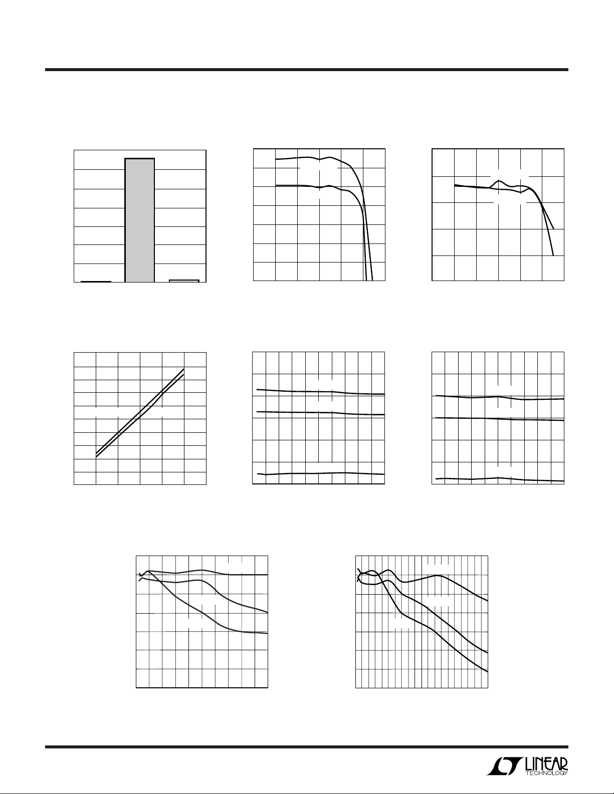
TYPICAL PERFOR A CE CHARACTERISTICS
Grounded Input Histogram
35000
30000
25000
20000
COUNT
15000
10000
5000
0
2041
Power vs Sample Rate,
Input Frequency = 5MHz
500
480
460
440
420
400
380
POWER (mW)
360
340
320
300
0
10
20
SAMPLE RATE (Msps)
2042 2043
CODE
2V RANGE3.2V RANGE
30 40
SNR vs Sample Rate,
Input Frequency = 5MHz, –1dB
73
3.2V RANGE
2V RANGE
20 30 40
10
SAMPLE RATE (Msps)
50 60
1745 G11
1745 G10
72
71
70
69
SNR (dBFS)
68
67
66
0
SNR vs Input Frequency
3.2V Range
80
75
–1dBFS
70
65
SNR (dB)
60
55
60
50
1745 G13
50
20 40 60 80
INPUT FREQUENCY (MHz)
–6dBFS
–20dBFS
10010030507090
1745 G14
SFDR vs Sample Rate,
Input Frequency = 5MHz, –1dB
110
100
90
SFDR (dB)
80
70
60
0
10
3.2V RANGE
2V RANGE
20 30 40
SAMPLE RATE (Msps)
SNR vs Input Frequency
2V Range
80
75
70
65
SNR (dB)
60
55
50
20 40 60 80
INPUT FREQUENCY (MHz)
–1dBFS
–6dBFS
–20dBFS
50 60
1745 G12
10010030507090
1745 G15
6
SFDR vs Input Frequency
and Amplitude, 3.2V Range
110
100
90
80
70
SFDR (dBFS)
60
50
40
0
10
20
INPUT FREQUENCY (MHz)
–6dBFS
–1dBFS
30
50
40
–20dBFS
70
60 80
90
1746 G16
100
SFDR vs Input Frequency
and Amplitude, 2V Range
110
100
90
80
70
SFDR (dBFS)
60
50
40
0
–1dBFS
50
INPUT FREQUENCY (MHz)
100
–20dBFS
–6dBFS
150
200
1745 G17
1745i

UW
TYPICAL PERFOR A CE CHARACTERISTICS
LTC1745
2nd and 3rd Harmonic vs Input
Frequency, 3.2V Range, –1dB
–30
–50
–70
–90
DISTORTION (dB)
–110
–130
3RD HARMONIC
10 20 30
0
2ND HARMONIC
60 70 90
40 50
INPUT FREQUENCY (MHz)
Worst Harmonic 4th or Higher vs
Input Frequency, 2V Range, –1dB
–60
–70
–80
2nd and 3rd Harmonic vs Input
Frequency, 2V Range, –1dB
–30
–50
–70
–90
DISTORTION (dB)
–110
80
100
1745 G18
–130
0
2ND HARMONIC
3ND HARMONIC
30 30 50
INPUT FREQUENCY (MHz)
40
1745 G19
Worst Harmonic 4th or Higher vs
Input Frequency, 3.2V Range, –1dB
–60
–70
–80
–90
DISTORTION (dB)
–100
–110
10 20 30
0
INPUT FREQUENCY (MHz)
40 50
60 70 90
80
100
1746 G20
SFDR vs Input Amplitude,
2V Range, 5MHz Input Frequency
110
100
SFDR dBFS
90
–90
DISTORTION (dB)
–100
–110
0
50 150 200
INPUT FREQUENCY (MHz)
100
1745 G21
80
SFDR (dBc AND dBFS)
70
60
–60
INPUT AMPLITUDE (dBFS)
–40
SFDR dBc
–20
0
1745 G22
1745i
7

LTC1745
UUU
PI FU CTIO S
SENSE (Pin 1): Reference Sense Pin. Ground selects
±1V. VDD selects ±1.6V. Greater than 1V and less than
1.6V applied to the SENSE pin selects an input range of
±V
VCM (Pin 2): 2.35V Output and Input Common Mode Bias.
Bypass to ground with 4.7µF ceramic chip capacitor.
GND (Pins 3, 6, 9, 12, 13, 16, 19, 21, 36, 37): ADC
Power Ground.
A
IN
A
IN
VDD (Pins 7, 8, 17, 18, 20): 5V Supply. Bypass to AGND
with 1µF ceramic chip capacitor.
REFLB (Pin 10): ADC Low Reference. Bypass to Pin 11
with 0.1µF ceramic chip capacitor. Do not connect to
Pin␣ 14.
REFHA (Pin 11): ADC High Reference. Bypass to Pin 10
with 0.1µF ceramic chip capacitor, to Pin 14 with a 4.7µF
ceramic capacitor and to ground with 1µF ceramic
capacitor.
REFLA (Pin 14): ADC Low Reference. Bypass to Pin 15
with 0.1µF ceramic chip capacitor, to Pin 11 with a 4.7µF
ceramic capacitor and to ground with 1µF ceramic
capacitor.
REFHB (Pin 15): ADC High Reference. Bypass to Pin 14
with 0.1µF ceramic chip capacitor. Do not connect to
Pin␣ 11.
, ±1.6V is the largest valid input range.
SENSE
+
(Pin 4): Positive Differential Analog Input.
–
(Pin 5): Negative Differential Analog Input.
MSBINV (Pin 22): MSB Inversion Control. Low inverts
the MSB, 2’s complement output format. High does not
invert the MSB, offset binary output format.
ENC (Pin 23): Encode Input. The input sample starts on
the positive edge.
ENC (Pin 24): Encode Complement Input. Conversion
starts on the negative edge. Bypass to ground with 0.1µF
ceramic for single-ended ENCODE signal.
OE (Pin 25): Output Enable. Low enables outputs. Logic
high makes outputs Hi-Z.
CLKOUT (Pin 26): Data Valid Output. Latch data on the
rising edge of CLKOUT.
OGND (Pins 27, 38, 47): Output Driver Ground.
NC (Pins 28, 29): Do Not Connect These Pins.
D0-D1 (Pins 30, 31): Digital Outputs. D0 is the LSB.
OVDD (Pins 32, 43): Positive Supply for the Output Driv-
ers. Bypass to ground with 0.1µF ceramic chip capacitor.
D2-D4 (Pins 33 to 35): Digital Outputs.
D5-D8 (Pins 39 to 42): Digital Outputs.
D9-D11 (Pins 44 to 46): Digital Outputs. D11 is the MSB.
OF (Pin 48): Over/Under Flow Output. High when an over
or under flow has occurred.
8
1745i

UWW
TI I G DIAGRA
LTC1745
ANALOG
INPUT
ENCODE
DATA
CLKOUT
OE
DATA
UU
N
t
3
t
6
t
5
t
7
t
2
DATA (N – 5)
D11 TO D0
DATA N
D11 TO D0, OF AND CLKOUT
W
FU CTIO AL BLOCK DIAGRA
t
1
t
4
DATA (N – 4)
D11 TO D0
t
8
DATA (N – 3)
D11 TO D0
1745 TD
±1V
DIFFERENTIAL
ANALOG INPUT
SENSE
4.7µF
OV
DD
+
A
IN
S/H
–
A
IN
BUFFER
RANGE
SELECT
V
CM
2.35V
REF
AMP
DIFF AMP
0.1µF 0.1µF
12-BIT
PIPELINED ADC
REFHAREFLB
1µF1µF
REFLA REFHB
4.7µF
ENC
DIFFERENTIAL
ENCODE INPUT
12
OUTPUT
LATCHES
CONTROL LOGIC
ENC
OF
D11
•
•
•
D0
CLKOUT
OGND
V
DD
GND
1745 BD
OEMSBINV
0.1µF
1µF 1µF 1µF
0.5V TO 5V
0.1µF
5V
1745i
9

LTC1745
WUUU
APPLICATIO S I FOR ATIO
DYNAMIC PERFORMANCE
Signal-to-Noise Plus Distortion Ratio
The signal-to-noise plus distortion ratio [S / (N + D)] is the
ratio between the RMS amplitude of the fundamental input
frequency and the RMS amplitude of all other frequency
components at the ADC output. The output is band limited
to frequencies above DC to below half the sampling
frequency.
Signal-to-Noise Ratio
The signal-to-noise ratio (SNR) is the ratio between the
RMS amplitude of the fundamental input frequency and
the RMS amplitude of all other frequency components
except the first five harmonics and DC.
Total Harmonic Distortion
Total harmonic distortion is the ratio of the RMS sum of all
harmonics of the input signal to the fundamental itself. The
out-of-band harmonics alias into the frequency band
between DC and half the sampling frequency. THD is
expressed as:
If two pure sine waves of frequencies fa and fb are applied
to the ADC input, nonlinearities in the ADC transfer function can create distortion products at the sum and difference frequencies of mfa ± nfb, where m and n = 0, 1, 2, 3,
etc. The 3rd order intermodulation products are 2fa + fb,
2fb + fa, 2fa – fb and 2fb – fa. The intermodulation
distortion is defined as the ratio of the RMS value of either
input tone to the RMS value of the largest 3rd order
intermodulation product.
Spurious Free Dynamic Range (SFDR)
Spurious free dynamic range is the peak harmonic or
spurious noise that is the largest spectral component
excluding the input signal and DC. This value is expressed
in decibels relative to the RMS value of a full scale input
signal.
Input Bandwidth
The input bandwidth is that input frequency at which the
amplitude of the reconstructed fundamental is reduced by
3dB for a full scale input signal.
Aperture Delay Time
222 2
VVV Vn
+++
THD Log
=
20
where V1 is the RMS amplitude of the fundamental frequency and V2 through Vn are the amplitudes of the
second through nth harmonics. The THD calculated in this
data sheet uses all the harmonics up to the fifth.
Intermodulation Distortion
If the ADC input signal consists of more than one spectral
component, the ADC transfer function nonlinearity can
produce intermodulation distortion (IMD) in addition to
THD. IMD is the change in one sinusoidal input caused by
the presence of another sinusoidal input at a different
frequency.
234
V
1
...
The time from when a rising ENC equals the ENC voltage
to the instant that the input signal is held by the sample and
hold circuit.
Aperture Delay Jitter
The variation in the aperture delay time from conversion to
conversion. This random variation will result in noise
when sampling an AC input. The signal to noise ratio due
to the jitter alone will be:
SNR
= –20log (2π) • FIN • T
JITTER
JITTER
10
1745i

WUUU
APPLICATIO S I FOR ATIO
LTC1745
CONVERTER OPERATION
As shown in Figure 1, the LTC1745 is a CMOS pipelined
multistep converter. The converter has four pipelined ADC
stages; a sampled analog input will result in a digitized
value five cycles later, see the Timing Diagram section.
The analog input is differential for improved common
mode noise immunity and to maximize the input range.
Additionally, the differential input drive will reduce even
order harmonics of the sample-and-hold circuit. The encode input is also differential for improved common mode
noise immunity.
The LTC1745 has two phases of operation, determined by
the state of the differential ENC/ENC input pins. For
+
A
IN
INPUT
S/H
–
A
IN
FIRST STAGE
5-BIT
PIPELINED
ADC STAGE
SECOND STAGE THIRD STAGE FOURTH STAGE
4-BIT
PIPELINED
ADC STAGE
brevity, the text will refer to ENC greater than ENC as ENC
high and ENC less than ENC as ENC low.
Each pipelined stage shown in Figure 1 contains an ADC,
a reconstruction DAC and an interstage residue amplifier.
In operation, the ADC quantizes the input to the stage and
the quantized value is subtracted from the input by the
DAC to produce a residue. The residue is amplified and
output by the residue amplifier. Successive stages operate
out of phase so that when the odd stages are outputting
their residue, the even stages are acquiring that residue
and visa versa.
4-BIT
PIPELINED
ADC STAGE
4-BIT
FLASH
ADC
V
4.7µF
SENSE
CM
2.35V
REFERENCE
RANGE
SELECT
REF
BUF
INTERNAL
REFERENCES TO ADC
DIFF
REF
AMP
REFHAREFLB
0.1µF 0.1µF
1µF1µF
REFLA REFHB
4.7µF
INTERNAL
CLOCK SIGNALS
DIFFERENTIAL
INPUT
LOW JITTER
CLOCK
DRIVER
ENC ENC
CONTROL
MSBINV
LOGIC
SHIFT REGISTER AND CORRECTION
OUTPUT
DRIVERS
OE
OGND
OV
DD
0.5V TO
5V
OF
D11
•
•
•
D0
CLKOUT
1745 F01
Figure 1. Functional Block Diagram
1745i
11

LTC1745
WUUU
APPLICATIO S I FOR ATIO
When ENC is low, the analog input is sampled differentially
directly onto the input sample-and-hold capacitors, inside
the “Input S/H” shown in the block diagram. At the instant
that ENC transitions from low to high, the sampled input
is held. While ENC is high, the held input voltage is
buffered by the S/H amplifier which drives the first pipelined
ADC stage. The first stage acquires the output of the S/H
during this high phase of ENC. When ENC goes back low,
the first stage produces its residue which is acquired by
the second stage. At the same time, the input S/H goes
back to acquiring the analog input. When ENC goes back
high, the second stage produces its residue which is
acquired by the third stage. An identical process is repeated for the third stage, resulting in a third stage residue
that is sent to the fourth stage ADC for final evaluation.
Each ADC stage following the first has additional range to
accommodate flash and amplifier offset errors. Results
from all of the ADC stages are digitally delayed such that
the results can be properly combined in the correction
logic before being sent to the output buffer.
acquire a new sample. Since the sampling capacitors still
hold the previous sample, a charging glitch proportional to
the change in voltage between samples will be seen at this
time. If the change between the last sample and the new
sample is small the charging glitch seen at the input will be
small. If the input change is large, such as the change seen
with input frequencies near Nyquist, then a larger charging
glitch will be seen.
Common Mode Bias
The ADC sample-and-hold circuit requires differential drive
to achieve specified performance. Each input should swing
±0.8V for the 3.2V range or ±0.5V for the 2V range, around
a common mode voltage of 2.35V. The VCM output pin
(Pin␣ 2) may be used to provide the common mode bias
level. VCM can be tied directly to the center tap of a transformer to set the DC input level or as a reference level to
an op amp differential driver circuit. The VCM pin must be
bypassed to ground close to the ADC with 4.7µF or greater
capacitor.
SAMPLE/HOLD OPERATION AND INPUT DRIVE
Sample Hold Operation
Figure 2 shows an equivalent circuit for the LTC1745
CMOS differential sample-and-hold. The differential analog inputs are sampled directly onto sampling capacitors
(C
SAMPLE
) through CMOS transmission gates. This direct
capacitor sampling results in lowest possible noise for a
given sampling capacitor size. The capacitors shown
attached to each input (C
PARASITIC
) are the summation of
all other capacitance associated with each input.
During the sample phase when ENC/ENC is low, the
transmission gate connects the analog inputs to the sampling capacitors and they charge to, and track the differential input voltage. When ENC/ENC transitions from low to
high the sampled input voltage is held on the sampling
capacitors. During the hold phase when ENC/ENC is high
the sampling capacitors are disconnected from the input
and the held voltage is passed to the ADC core for
processing. As ENC/ENC transitions from high to low the
inputs are reconnected to the sampling capacitors to
A
IN
A
IN
ENC
ENC
LTC1745
V
DD
+
C
PARASITIC
4pF
V
DD
–
C
PARASITIC
4pF
5V
BIAS
2V
6k
6k
2V
Figure 2. Equivalent Input Circuit
C
SAMPLE
4pF
C
SAMPLE
4pF
1745 F02
12
1745i

WUUU
APPLICATIO S I FOR ATIO
LTC1745
Input Drive Impedance
As with all high performance, high speed ADCs the dynamic performance of the LTC1745 can be influenced by
the input drive circuitry, particularly the second and third
harmonics. Source impedance and input reactance can
influence SFDR. At the falling edge of encode the sampleand-hold circuit will connect the 4pF sampling capacitor to
the input pin and start the sampling period. The sampling
period ends when encode rises, holding the sampled input
on the sampling capacitor. Ideally the input circuitry
should be fast enough to fully charge the sampling capacitor during the sampling period 1/(2F
ENCODE
); however,
this is not always possible and the incomplete settling may
degrade the SFDR. The sampling glitch has been designed
to be as linear as possible to minimize the effects of
incomplete settling.
For the best performance, it is recomended to have a
source impedence of 100Ω or less for each input. The S/H
circuit is optimized for a 50Ω source impedance. If the
source impedance is less than 50Ω, a series resistor
should be added to increase this impedance to 50Ω. The
source impedence should be matched for the differential
inputs. Poor matching will result in higher even order
harmonics, especially the second.
Input Drive Circuits
Figure 3 shows the LTC1745 being driven by an RF
transformer with a center tapped secondary. The secondary center tap is DC biased with VCM, setting the ADC input
signal at its optimum DC level. Figure 3 shows a 1:1 turns
ratio transformer. Other turns ratios can be used if the
source impedence seen by the ADC does not exceed
100Ω for each ADC input. A disadvantage of using a
transformer is the loss of low frequency response. Most
small RF transformers have poor performance at frequencies below 1MHz.
Figure 4 demonstrates the use of operational amplifiers to
convert a single ended input signal into a differential input
signal. The advantage of this method is that it provides low
frequency input response; however, the limited gain bandwidth of most op amps will limit the SFDR at high input
frequencies.
The 25Ω resistors and 12pF capacitors on the analog
inputs serve two purposes: isolating the drive circuitry
from the sample-and-hold charging glitches and limiting
the wideband noise at the converter input. For input
frequencies higher than 50MHz, the capacitors may need
to be decreased to prevent excessive signal loss.
ANALOG
INPUT
4.7µF
0.1µF
1:1
100Ω 100Ω 12pF
25Ω
25Ω
12pF
25Ω
25Ω
12pF
Figure 3. Single-Ended to Differential
Conversion Using a Transformer
V
CM
25Ω
12pF
4.7µF
12pF
12pF
+
A
IN
LTC1745
–
A
IN
1745 F04
5V
SINGLE-ENDED
V
CM
INPUT
2.35V ±1/2
RANGE
+
1/2 LT1810
25Ω
–
LTC1745
+
A
IN
–
A
IN
100Ω
+
1/2 LT1810
25Ω 25Ω
–
1745 F03
500Ω 500Ω
Figure 4. Differential Drive with Op Amps
1745i
13

LTC1745
V
CM
SENSE
2.35V
1.1V
4.7µF
12.5k
1µF
11k
1745 F06a
LTC1745
WUUU
APPLICATIO S I FOR ATIO
Reference Operation
Figure 5 shows the LTC1745 reference circuitry consisting
of a 2.35V bandgap reference, a difference amplifier and
switching and control circuit. The internal voltage reference can be configured for two pin selectable input ranges
of 2V(±1V differential) or 3.2V(±1.6V differential). Tying
the SENSE pin to ground selects the 2V range; tying the
SENSE pin to VDD selects the 3.2V range.
The 2.35V bandgap reference serves two functions: its
output provides a DC bias point for setting the common
mode voltage of any external input circuitry; additionally,
the reference is used with a difference amplifier to generate the differential reference levels needed by the internal
ADC circuitry.
An external bypass capacitor is required for the 2.35V
reference output, VCM. This provides a high frequency low
impedance path to ground for internal and external circuitry. This is also the compensation capacitor for the
reference. It will not be stable without this capacitor.
The difference amplifier generates the high and low reference for the ADC. High speed switching circuits are
connected to these outputs and they must be externally
bypassed. Each output has two pins: REFHA and REFHB
for the high reference and REFLA and REFLB for the low
reference. The doubled output pins are needed to reduce
package inductance. Bypass capacitors must be connected as shown in Figure 5.
Other voltage ranges in between the pin selectable ranges
can be programmed with two external resistors as shown
in Figure 6a. An external reference can be used by applying
its output directly or through a resistor divider to SENSE.
It is not recommended to drive the SENSE pin with a logic
device since the logic threshold is close to ground and
VDD. The SENSE pin should be tied high or low as close to
the converter as possible. If the SENSE pin is driven
externally, it should be bypassed to ground as close to the
device as possible with a 1µF ceramic capacitor.
FOR 3.2V RANGE;
TIE TO V
DD
TIE TO GND FOR 2V RANGE;
RANGE = 2 • V
1V < V
SENSE
SENSE
Figure 5. Equivalent Reference Circuit
14
2.35V
FOR
< 1.6V
1µF
1µF
0.1µF
4.7µF
4.7µF
SENSE
REFLB
REFHA
REFLA
0.1µF
REFHB
LTC1745
4Ω
V
CM
RANGE
DETECT
AND
CONTROL
2.35V BANDGAP
REFERENCE
1.6V
INTERNAL ADC
HIGH REFERENCE
DIFF AMP
INTERNAL ADC
LOW REFERENCE
1V
BUFFER
1745 F05
Figure 6a. 2.2V Range ADC
V
4.7µF
SENSE
1µF0.1µF
CM
LTC1745
1745 F06b
2.35V
5V
LT1790-1.25
1.25V64
1, 2
Figure 6b. 2.5V Range ADC with an External Reference
1745i

WUUU
APPLICATIO S I FOR ATIO
LTC1745
Input Range
The input range can be set based on the application. For
oversampled signal processing in which the input frequency is low (<10MHz), the largest input range will
provide the best signal-to-noise performance while maintaining excellent SFDR. For high input frequencies
(>10MHz), the 2V range will have the best SFDR performance but the SNR will degrade by 1.5dB. See the Typical
Performance Characteristics section.
LTC1745
2V BIAS
V
DD
CLOCK
INPUT
ANALOG INPUT
0.1µF
1:4
50Ω
ENC
ENC
2V BIAS
V
DD
Driving the Encode Inputs
The noise performance of the LTC1745 can depend on the
encode signal quality as much as on the analog input. The
ENC/ENC inputs are intended to be driven differentially,
primarily for noise immunity from common mode noise
sources. Each input is biased through a 6k resistor to a 2V
bias. The bias resistors set the DC operating point for
transformer coupled drive circuits and can set the logic
threshold for single-ended drive circuits.
5V
BIAS
TO INTERNAL
ADC CIRCUITS
6k
6k
Figure 7. Transformer Driven ENC/ENC with Equivalent Encode Input Circuit
V
THRESHOLD
= 2V
0.1µF
ENC
ENC2V
LTC1745
Figure 8a. Single-Ended ENC Drive,
Not Recommended for Low Jitter
1745 F08a
1745 F07
3.3V
MC100LVELT22
3.3V
130Ω
Q0
D0
Q0
130Ω
83Ω83Ω
ENC
ENC
LTC1745
1745 F08b
Figure 8b. ENC Drive Using a CMOS-to-PECL Translator
1745i
15

LTC1745
WUUU
APPLICATIO S I FOR ATIO
Any noise present on the encode signal will result in
additional aperture jitter that will be RMS summed with the
inherent ADC aperture jitter.
In applications where jitter is critical (high input frequencies) take the following into consideration:
1. Differential drive should be used.
2. Use as large an amplitude as possible; if transformer
coupled use a higher turns ratio to increase the
amplitude.
3. If the ADC is clocked with a sinusoidal signal, filter the
encode signal to reduce wideband noise.
4. Balance the capacitance and series resistance at both
encode inputs so that any coupled noise will appear at
both inputs as common mode noise.
The encode inputs have a common mode range of 1.8V to
VDD. Each input may be driven from ground to VDD for
single-ended drive.
Maximum and Minimum Encode Rates
The maximum encode rate for the LTC1745 is 25Msps. For
the ADC to operate properly the encode signal should have
a 50% (±5%) duty cycle. Each half cycle must have at least
19ns for the ADC internal circuitry to have enough settling
time for proper operation. Achieving a precise 50% duty
cycle is easy with differential sinusoidal drive using a
transformer or using symmetric differential logic such as
PECL or LVDS. When using a single-ended encode signal
asymmetric rise and fall times can result in duty cycles that
are far from 50%.
At sample rates slower than 25Msps the duty cycle can
vary from 50% as long as each half cycle is at least 19ns.
The lower limit of the LTC1745 sample rate is determined
by the droop of the sample-and-hold circuits. The pipelined
architecture of this ADC relies on storing analog signals
on small valued capacitors. Junction leakage will discharge the capacitors. The specified minimum operating
frequency for the LTC1745 is 1Msps.
DIGITAL OUTPUTS
Digital Output Buffers
Figure 9 shows an equivalent circuit for a single output
buffer. Each buffer is powered by OVDD and OGND, isolated from the ADC power and ground. The additional
N-channel transistor in the output driver allows operation
down to low voltages. The internal resistor in series with
the output makes the output appear as 50Ω to external
circuitry and may eliminate the need for external damping
resistors.
16
DATA
FROM
LATCH
OE
LTC1745
V
DD
PREDRIVER
LOGIC
Figure 9. Equivalent Circuit for a Digital Output Buffer
V
DD
OV
DD
43Ω
1745 F09
OV
DD
OGND
0.5V TO
V
DD
0.1µF
TYPICAL
DATA
OUTPUT
1745i

WUUU
APPLICATIO S I FOR ATIO
LTC1745
Output Loading
As with all high speed/high resolution converters the
digital output loading can affect the performance. The
digital outputs of the LTC1745 should drive a minimal
capacitive load to avoid possible interaction between the
digital outputs and sensitive input circuitry. The output
should be buffered with a device such as an ALVCH16373
CMOS latch. For full speed operation the capacitive load
should be kept under 10pF. A resistor in series with the
output may be used but is not required since the ADC has
a series resistor of 43Ω on chip.
Lower OVDD voltages will also help reduce interference
from the digital outputs.
Format
The LTC1745 parallel digital output can be selected for
offset binary or 2’s complement format. The format is
selected with the MSBINV pin; high selects offset binary.
Overflow Bit
An overflow output bit indicates when the converter is
overranged or underranged. When OF outputs a logic high
the converter is either overranged or underranged.
Output Clock
The ADC has a delayed version of the ENC input available
as a digital output, CLKOUT. The CLKOUT pin can be used
to synchronize the converter data to the digital system.
This is necessary when using a sinusoidal encode. Data
will be updated just after CLKOUT falls and can be latched
on the rising edge of CLKOUT.
Output Driver Power
Separate output power and ground pins allow the output
drivers to be isolated from the analog circuitry. The power
supply for the digital output buffers, OVDD, should be tied
to the same power supply as for the logic being driven. For
example if the converter is driving a DSP powered by a 3V
supply then OVDD should be tied to that same 3V supply.
OVDD can be powered with any voltage up to 5V. The logic
outputs will swing between OGND and OVDD.
Output Enable
The outputs may be disabled with the output enable pin,
OE. OE low disables all data outputs including OF and
CLKOUT. The data access and bus relinquish times are too
slow to allow the outputs to be enabled and disabled
during full speed operation. The output Hi-Z state is
intended for use during long periods of inactivity.
GROUNDING AND BYPASSING
The LTC1745 requires a printed circuit board with a clean
unbroken ground plane. A multilayer board with an internal ground plane is recommended. The pinout of the
LTC1745 has been optimized for a flowthrough layout so
that the interaction between inputs and digital outputs is
minimized. Layout for the printed circuit board should
ensure that digital and analog signal lines are separated as
much as possible. In particular, care should be taken not
to run any digital track alongside an analog signal track or
underneath the ADC.
1745i
17

LTC1745
WUUU
APPLICATIO S I FOR ATIO
High quality ceramic bypass capacitors should be used at
the V
DD, VCM
shown in the block diagram on the front page of this data
sheet. Bypass capacitors must be located as close to the
pins as possible. Of particular importance are the capacitors between REFHA and REFLB and between REFHB and
REFLA. These capacitors should be as close to the device
as possible (1.5mm or less). Size 0402 ceramic capacitors
are recomended. The large 4.7µF capacitor between REFHA
and REFLA can be somewhat further away. The traces
connecting the pins and bypass capacitors must be kept
short and should be made as wide as possible.
The LTC1745 differential inputs should run parallel and
close to each other. The input traces should be as short as
possible to minimize capacitance and to minimize noise
pickup.
, REFHA, REFHB, REFLA and REFLB pins as
An analog ground plane separate from the digital processing system ground should be used. All ADC ground pins
labeled GND should connect to this plane. All ADC V
bypass capacitors, reference bypass capacitors and input
filter capacitors should connect to this analog plane. The
LTC1745 has three output driver ground pins, labeled
OGND (Pins 27, 38 and 47). These grounds should connect to the digital processing system ground. The output
driver supply, OVDD should be connected to the digital
processing system supply. OVDD bypass capacitors should
bypass to the digital system ground. The digital processing system ground should be connected to the analog
plane at ADC OGND (Pin 38).
DD
18
1745i

PACKAGE DESCRIPTIO
0.95 ±0.10
U
FW Package
48-Lead Plastic TSSOP (6.1mm)
(Reference LTC DWG # 05-08-1651)
48 46 4544434241 40 39 38 37 36 35 34 33 32 31 30 29 28 27 26 2547
12.4 – 12.6*
(.488 – .496)
LTC1745
8.1 ±0.10
0.32 ±0.05 0.50 TYP
RECOMMENDED SOLDER PAD LAYOUT
6.0 – 6.2**
(.236 – .244)
0.09 – 0.20
(.0035 – .008)
NOTE:
1. CONTROLLING DIMENSION: MILLIMETERS
2. DIMENSIONS ARE IN
3. DRAWING NOT TO SCALE
*
DIMENSIONS DO NOT INCLUDE MOLD FLASH. MOLD FLASH SHALL NOT EXCEED .152mm (.006") PER SIDE
**
DIMENSIONS DO NOT INCLUDE INTERLEAD FLASH. INTERLEAD FLASH SHALL NOT EXCEED .254mm (.010") PER SIDE
0.45 – 0.75
(.018 – .029)
MILLIMETERS
(INCHES)
6.2 ±0.10
° – 8°
0
1345678 9 10 11 12 13 14 15 16 17 18 19 20 21 22 23 24
2
-C-
0.50
(.0197)
BSC
0.17 – 0.27
(.0067 – .0106)
(.311 – .327)
1.20
(.0473)
MAX
0.05 – 0.15
(.002 – .006)
7.9 – 8.3
FW48 TSSOP 0502
-TC.10
1745i
19

LTC1745
RELATED PARTS
PART NUMBER DESCRIPTION COMMENTS
LT1019 Precision Bandgap Reference 0.05% Max Initial Accuracy, 5ppm/°C Max Drift
LTC1196 8-Bit, 1Msps Serial ADC 3V to 5V, SO-8
LTC1405 12-Bit, 5Msps, Sampling ADC 5V or ±5V Pin Compatible with the LTC1420
LTC1406 8-Bit, 20Msps ADC Undersampling Capability Up to 70MHz Input
LTC1410 12-Bit, 1.25Msps ADC ±5V, 71dB SINAD
LTC1411 14-Bit, 2.5Msps ADC 5V, No Pipeline Delay, 80dB SINAD
LTC1412 12-Bit, 3Msps, Sampling ADC ±5V, No Pipeline Delay, 72dB SINAD
LTC1414 14-Bit, 2.2Msps ADC ±5V, 81dB SINAD and 95dB SFDR
LTC1415 Single 5V, 12-Bit, 1.25Msps 55mW Power Dissipation, 72dB SINAD
LTC1419 14-Bit, 800ksps ADC ±5V, 95dB SFDR
LTC1420 12-Bit, 10Msps ADC 71dB SINAD and 83dB SFDR at Nyquist
LT1460 Micropower Precision Series Reference 0.075% Accuracy, 10ppm/°C Drift
LTC1604/LTC1608 16-Bit, 333ksps/500ksps ADCs 16-Bit, No Missing Codes, 90dB SINAD, –100dB THD
LTC1668 16-Bit, 50Msps DAC 87dB SFDR at 1MHz f
LTC1740 14-Bit, 6Msps ADC Low Power, 79dB SINAD, 91dB SFDR
LTC1743 12-Bit, 50Msps ADC 72.5dB SNR, 87dB SFDR, Pin Compatible with LTC1744, LTC1745, LTC1746
LTC1744 14-Bit, 50Msps ADC 77dB SNR, Undersampling to 70MHz, Pin Compatible with LTC1743, LTC1745, LTC1746
LTC1746 14-Bit, 25Msps ADC Low Power, 77.5dB SNR, 99dB SFDR Pin Compatible with Family
, Low Power, Low Cost
OUT
20
Linear Technology Corporation
1630 McCarthy Blvd., Milpitas, CA 95035-7417
(408) 432-1900 ● FAX: (408) 434-0507
●
www.linear.com
1745i
LT/TP 0103 1.5K • PRINTED IN THE USA
LINEAR TECHNOLOGY CORPORATION 2003
 Loading...