

Lithium-Ion Battery Charger with
FEATURES
■
Complete Linear Charger for 1-Cell Lithium-Ion
Batteries
■
Thermal Regulation Maximizes Charging Rate
without Risk of Overheating*
■
No External MOSFET, Sense Resistor or Blocking
Diode Required
■
Up to 1.5A Charge Current
■
Preset Charge Voltage with 1% Accuracy
■
Programmable Charge Current with 7% Accuracy
■
Programmable Charge Termination Timer
■
Tiny Thermally Enhanced 10-Pin MSOP Package
■
Charge Current Monitor Useful for Gas Gauging*
■
C/10 Charge Current Detection Output
■
Automatic Recharge
■
Thermistor Input for Temperature Qualified Charging
■
AC Present Logic Output
■
4.1V/4.2V Pin Selectable Output Voltage
U
APPLICATIO S
LTC1733
Monolithic Linear
Thermal Regulation
U
DESCRIPTIO
The LTC®1733 is a standalone constant-current/
constant-voltage linear charger for lithium-ion batteries
with an on-chip power MOSFET. Internal thermal feedback
regulates the charge current to limit die temperature
during high power operation or high ambient temperature
conditions. This feature allows the user to program a high
charge current without risk of damaging the LTC1733 or
the handheld product.
No external current sense resistor is needed and no
blocking diode is required due to the internal MOSFET
architecture. The charge current and charge time can be
set externally with a single resistor and capacitor, respectively. When the input supply (wall adapter) is removed,
the LTC1733 automatically enters a low current sleep
mode, dropping the battery drain current to less than 5µA.
The LTC1733 also includes NTC temperature sensing,
C/10 detection circuitry, AC present logic, 4.1V/4.2V pin
selectability and low battery charge conditioning (trickle
charging).
■
Cellular Telephones
■
Handheld Computers
■
Digital Still Cameras
■
Charging Docks and Cradles
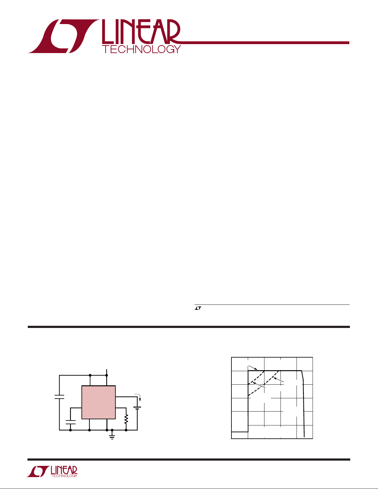
TYPICAL APPLICATIO
Standalone Li-Ion Battery Charger
V
= 5V
IN
28
V
SEL
4.7µF
4
TIMER
GND
0.1µF
*AN OUTPUT CAPACITOR MAY BE REQUIRED
DEPENDING ON BATTERY LEAD LENGTH
LTC1733
5
CC
BAT
PROG
NTC
6
The LTC1733 is available in a 10-pin thermally enhanced
MSOP package.
, LTC and LT are registered trademarks of Linear Technology Corporation.
*Patent Pending
U
Charge Current vs Battery Voltage
1200
1000
I
= 1A
BAT
9
1.5k
1%
1733TA01
4.2V
1-CELL
Li-Ion
BATTERY*
CHARGE CURRENT (mA)
7
800
600
400
200
TA = 0°C
TA = 25°C
CONSTANT
POWER
TRICKLE
0
2
CHARGE
VIN = 5V
= 40°C/W
θ
JA
2.5 3 4 4.5
BATTERY VOLTAGE (V)
CONSTANT
CURRENT
TA = 40°C
CONSTANT
VOLTAGE
3.5
1733 TA01b
sn1733 1733fs
1
LTC1733
WW
W
ABSOLUTE AXI U RATI GS
U
UUW
PACKAGE/ORDER I FOR ATIO
(Note 1)
Input Supply Voltage (VCC) ........................................ 7V
BAT............................................................................ 7V
NTC, SEL, TIMER, PROG ................ –0.3V to VCC + 0.3V
CHRG, FAULT, ACPR ...................................–0.3V to 7V
BAT Short-Circuit Duration ...........................Continuous
BAT Current (Note 2) .............................................. 1.6A
PROG Current (Note 2) ........................................ 1.6mA
Junction Temperature........................................... 125°C
TOP VIEW
1
CHRG
2
V
CC
FAULT
3
TIMER
4
GND
5
MSE EXPOSED PAD PACKAGE
10-LEAD PLASTIC MSOP
T
= 125°C, θJA = 40°C/W (Note 4)
JMAX
EXPOSED PAD IS GROUND.
(MUST BE SOLDERED TO PCB
FOR MAXIMUM HEAT TRANSFER).
10
ACPR
9
BAT
8
SEL
7
PROG
6
NTC
ORDER PART
NUMBER
LTC1733EMSE
MSE PART MARKING
LTLX
Operating Temperature Range (Note 3) ...–40°C to 85°C
Storage Temperature Range ................. –65°C to 150°C
Consult LTC Marketing for parts specified with wider operating temperature ranges.
Lead Temperature (Soldering, 10 sec).................. 300°C
ELECTRICAL CHARACTERISTICS
temperature range, otherwise specifications are at TA = 25°C. VCC = 5V
SYMBOL PARAMETER CONDITIONS MIN TYP MAX UNITS
V
CC
I
CC
V
BAT
I
BAT
I
TRIKL
V
TRIKL
∆V
TRIKL
V
UV
∆V
UV
V
MSD
V
MSD-HYS
V
ASD
VCC Supply Voltage ● 4.5 6.5 V
VCC Supply Current Charger On; Current Mode; R
Shutdown Mode; V
V
Regulated Output Voltage SEL = 0V ● 4.059 4.1 4.141 V
BAT
Battery Pin Current R
Trickle Charge Current V
Trickle Charge Trip Threshold V
Trickle Charge Trip Hysteresis 100 mV
VCC Undervoltage Lockout Voltage VCC Rising ● 4.2 4.5 V
VCC Undervoltage Lockout Hysteresis 150 mV
Manual Shutdown Threshold Voltage PROG Pin Voltage Rising 2.15 V
Manual Shutdown Hysteresis Voltage 100 mV
Automatic Shutdown Threshold Voltage (VCC - V
SEL = V
R
Shutdown Mode; V
Sleep Mode V
(V
The ● denotes the specifications which apply over the full operating
= 30k (Note 5) ● 13 mA
PROG
= 3V ● 0.9 2 mA
PROG
CC
= 3k; Current Mode ● 465 500 535 mA
PROG
= 1k; Current Mode 1.395 1.5 1.605 A
PROG
CC
< 2V; R
BAT
BAT
CC
PROG
Rising 2.48 V
) Voltage Falling 30 mV
BAT
- V
) Voltage Rising 60 mV
BAT
= 3V ±1 ±5 µA
PROG
< V
or VCC < (VUV – ∆VUV) ±1 ±5 µA
BAT
= 3k ● 35 50 65 mA
● 4.158 4.2 4.242 V
2
sn1733 1733fs
LTC1733
ELECTRICAL CHARACTERISTICS
TA = 25°C. VCC = 5V unless otherwise noted.
SYMBOL PARAMETER CONDITIONS MIN TYP MAX UNITS
V
PROG
I
CHRG
V
CHRG
V
ACPR
V
FAULT
I
C/10
t
TIMER
V
RECHRG
PROG Pin Voltage R
CHRG Pin Weak Pulldown Current V
CHRG Pin Output Low Voltage I
ACPR Pin Output Low Voltage I
FAULT Pin Output Low Voltage I
End of Charge Indication Current Level R
TIMER Accuracy C
= 3k, I
PROG
= 1V 25 µA
CHRG
= 5mA 0.35 V
CHRG
= 5mA 0.35 V
ACPR
= 5mA 0.35 V
FAULT
= 3k 35 50 65 mA
PROG
= 0.1µF ±10 %
TIMER
= 500µA; Current Mode 1.5 V
PROG
Recharge Battery Voltage Threshold Battery Voltage Falling, SEL = 0V 3.9 V
Battery Voltage Falling, SEL = 5V 4.0 V
V
NTC-HOT
V
HOT-HYS
V
NTC-COLD
V
COLD-HYS
V
NTC-DIS
V
DIS-HYS
V
SEL-IL
V
SEL-IH
T
LIM
NTC Pin Hot Threshold Voltage V
Falling 2.5 V
NTC
NTC Pin Hot Hysteresis Voltage 70 mV
NTC Pin Cold Threshold Voltage V
Rising 4.375 V
NTC
NTC Pin Cold Hystersis Voltage 70 mV
NTC Pin Disable Threshold Voltage V
Rising 100 mV
NTC
NTC Pin Disable Hystersis Voltage 10 mV
SEL Pin Threshold Input Low 0.3 V
SEL Pin Threshold Input High 1V
Junction Temperature in 105 °C
Constant-Temperature Mode
R
ON
Note 1: Absolute Maximum Ratings are those values beyond which the life
of a device may be impaired.
Note 2: The Absolute Maximum BAT Current Rating of 1.6A is guaranteed
by design and current density calculations. The Absolute Maximum PROG
Current Rating is guaranteed to be 1/1000 of BAT current rating by design.
Note 3: The LTC1733E is guaranteed to meet performance specifications
Power MOSFET “ON” Resistance 375 mΩ
temperature range are assured by design, characterization and correlation
with statistical process controls.
Note 4: Failure to solder the exposed backside of the package to the PC
board will result in a thermal resistance much higher than 40°C/W.
Note 5: Supply current includes PROG pin current but does not include
any current delivered to the battery through the BAT pin.
from 0°C to 70°C. Specifications over the –40°C to 85°C operating
sn1733 1733fs
3
LTC1733
VCC (V)
4.24
4.22
4.20
4.18
4.16
4.14
4.12
4.10
4.08
4.06
V
BAT
(V)
1733 G03
4.0 4.5 5.0
5.5
6.0 6.5 7.0
V
SEL
= V
CC
V
SEL
= 0V
TA = 25°C
I
BAT
= 10mA
R
PROG
= 1.5k
UW
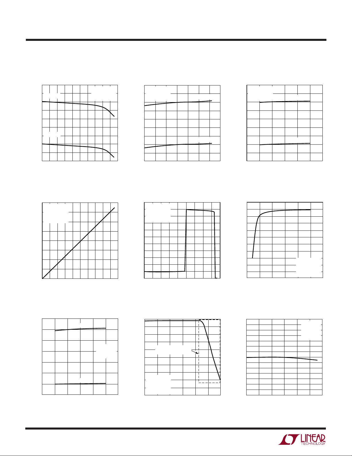
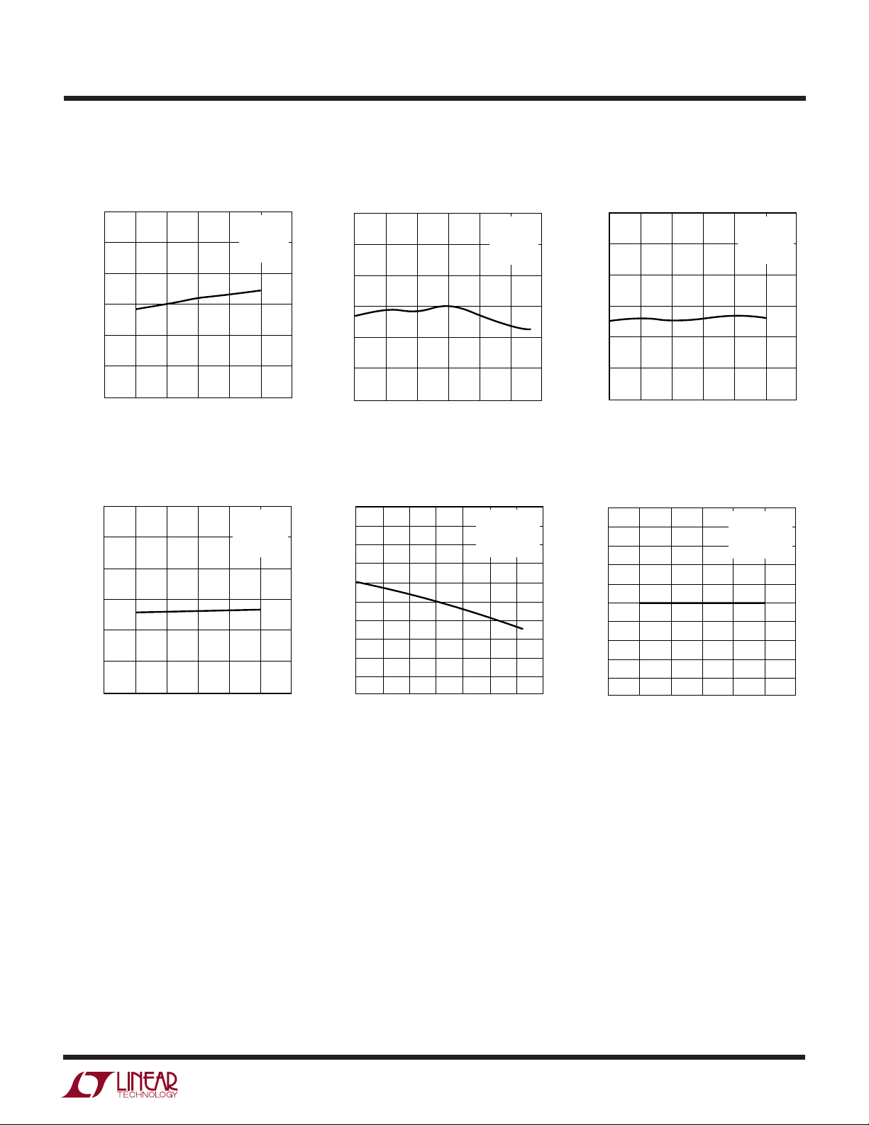
TYPICAL PERFOR A CE CHARACTERISTICS
Battery Regulation Voltage vs
Battery Charge Current
4.24
4.22
V
= 5V
SEL
4.20
4.18
4.16
(V)
BAT
4.14
V
V
= 0V
SEL
4.12
4.10
4.08
4.06
0 100 200 300
400
500
I
(mA)
BAT
PROG Pin Voltage vs Charge
Current
1.6
VCC = 5V
= 25°C
T
A
1.4
R
= 1.5k
PROG
V
= 5V
SEL
1.2
1.0
(V)
0.8
PROG
V
0.6
0.4
0.2
0
0 100 200 300
400
500
CHARGE CURRENT (mA)
VCC = 5V
= 25°C
T
A
= 1.5k
R
PROG
600 700 800 900 1000
1733 G01
600 700 800 900 1000
1733 G04
Battery Regulation Voltage vs
Temperature
4.24
VCC = 5V
= 10mA
I
4.22
BAT
= 1.5k
R
PROG
4.20
4.18
4.16
(V)
BAT
4.14
V
4.12
4.10
4.08
4.06
–50 –25 0
25
50 75 100 125
TEMPERATURE(°C)
Charge Current vs Battery Voltage
1100
VCC = 5V
1000
= 25°C
T
A
= 1.5k
R
PROG
900
800
700
600
(mA)
500
BAT
I
400
300
200
100
V
0
0
= 5V
SEL
0.5 1.5
1.0
2.5 4.5
BAT
3.0
(V)
2.0
V
Battery Regulation Voltage vs V
V
= 5V
SEL
V
= 0V
SEL
1733 G02
CC
Charge Current vs Input Voltage
1100
1000
900
800
700
600
(mA)
500
BAT
I
400
3.5
4.0
1733 G05
300
200
100
0
4.0
4.5 5.5
5.0
VCC (V)
6.0
V
T
R
V
BAT
A
PROG
SEL
= 4.1V
= 25°C
= 5V
= 1.5k
6.5
1733 G06
7.0
Charge Current vs V
1100
1000
900
800
(mA)
700
BAT
I
600
500
400
4.0
4
R
PROG
R
PROG
4.5 5.5
5.0
VCC (V)
CC
= 1.5k
= 3k
6.0
V
BAT
T
A
V
SEL
= 3.5V
= 25°C
= V
6.5
1733 G07
Charge Current vs Temperature
with Thermal Regulation
1000
900
800
700
600
CC
7.0
500
(mA)
BAT
I
400
300
200
100
0
–50
VCC = 5V
= 3.5V
V
BAT
R
PROG
= 5V
V
SEL
THERMAL CONTROL
LOOP IN OPERATION
= 1.5k
–25 25
0
TEMPERATURE (°C)
75
50
100
1733 G08
Charge Current vs Temperature
535
530
525
520
515
510
505
(mA)
500
BAT
495
I
490
485
480
475
470
465
–50 25 75
–25 0
TEMPERATURE (°C)
VCC = 5V
= 4V
V
BAT
R
= 3k
PROG
V
= 5V
SEL
50 100
1733 G09
sn1733 1733fs
UW
TYPICAL PERFOR A CE CHARACTERISTICS
LTC1733
PROG Pin Voltage vs V
Constant Current Mode
1.515
1.510
1.505
(V)
1.500
PROG
V
1.495
1.490
1.485
4.0 5.5 6.5
4.5 5.0
VCC (V)
Trickle Charge Current vs V
13
12
11
10
9
(% OF PROGRAMMED CURRENT)
8
BAT
I
7
4.0 5.5 6.5
4.5 5.0
VCC (V)
CC
TA = 25°C
= 3.5V
V
BAT
R
= 3k
PROG
= 5V
V
SEL
6.0 7.0
1733 G10
CC
TA = 25°C
= 2V
V
BAT
= 1.5k
R
PROG
= 5V
V
SEL
6.0 7.0
1733 G13
PROG Pin Voltage vs Temperature
Constant Current Mode
1.515
1.510
1.505
(V)
1.500
PROG
V
1.495
1.490
1.485
–50 25 75
–25 0
TEMPERATURE (°C)
50 100
Timer Accuracy vs Temperature
105
104
103
102
101
(%)
100
TIMER
t
99
98
97
96
95
–50 –25 0
25
TEMPERATURE(°C)
VCC = 5V
I
V
C
50 75 100 125
VCC = 5V
V
R
V
BAT
SEL
TIMER
BAT
PROG
= 5V
SEL
= 0mA
= 5V
= 0.1µF
= 4V
= 3k
1733 G11
1733 G14
Trickle Charge Current vs
Temperature
130
120
110
(mA)
100
BAT
I
90
80
70
–50 25 75
–25 0
TEMPERATURE (°C)
Timer Accuracy vs V
105
104
103
102
101
(%)
100
TIMER
t
99
98
97
96
95
4.0 5.5 6.5
4.5 5.0
V
(V)
CC
VCC = 5V
= 2V
V
BAT
= 1.5k
R
PROG
= 5V
V
SEL
50 100
1733 G12
CC
TA = 25°C
= 0mA
I
BAT
= 5V
V
SEL
= 0.1µF
C
TIMER
6.0 7.0
1733 G15
sn1733 1733fs
5

LTC1733
U
UU
PI FU CTIO S
CHRG: Open-Drain Charge Status Output. When the
battery is being charged, the CHRG pin is pulled low by an
internal N-channel MOSFET. When the charge current
drops to 10% of the full-scale current, the N-channel
MOSFET latches off and a 25µA current source is con-
nected from the CHRG pin to ground. The C/10 latch can
be cleared by momentarily pulling the PROG pin above the
2.15V shutdown threshold, or by toggling VCC. When the
timer runs out or the input supply is removed, the current
source is disconnected and the CHRG pin is forced to a
high impedance state.
VCC: Positive Input Supply Voltage. When VCC is within
30mV of V
threshold, the LTC1733 enters sleep mode, dropping I
to less than 5µA. VCC can range from 4.5V to 6.5V. Bypass
this pin with at least a 4.7µF ceramic capacitor to ground.
FAULT: Open-Drain Fault Status Output. The FAULT opendrain logic signal indicates that the charger has timed out
under trickle charge conditions (1/4 of total time period) or
the NTC comparator is indicating an out-of-range battery
temperature condition. When V
trickle charging activates whereby the charge current
drops to one tenth of its programmed value and the timer
period is reduced by a factor of four. When one fourth of
the timing period has elapsed, if V
2.48V, trickle charging stops and the FAULT pin latches to
ground. The fault can be cleared by toggling VCC, momentarily pulling the PROG pin above the 2.15V shutdown
threshold, or pulling the BAT pin above 2.48V. If the NTC
comparator is indicating an out-of-range battery temperature condition, then the FAULT pin will pull to ground until
the temperature returns to the acceptable range.
TIMER: Timer Capacitor. The timer period is set by placing
a capacitor, C
Time (Hours) = (C
Short the TIMER pin to ground to disable the internal timer
function.
or less than the undervoltage lockout
BAT
is less that 2.48V,
BAT
is still less than
BAT
, to ground. The timer period is:
TIMER
• 3 hr)/(0.1µF)
TIMER
BAT
GND: Ground. Connect exposed back package to ground.
NTC: Input to the NTC (Negative Temperature Coefficient)
Thermistor Temperature Monitoring Circuit. With an external 10kΩ NTC thermistor to ground and a 1% resistor
to VCC, this pin can sense the temperature of the battery
pack and stop charging when it is out of range. When the
voltage at this pin drops below (0.5)•(VCC) at hot temperatures or rises above (0.875)•(VCC) at cold, charging is
suspended and the internal timer is frozen. The CHRG pin
output status is not affected in this hold state. The FAULT
pin is pulled to ground, but not latched. When the temperature returns to an acceptable range, charging will resume
and the FAULT pin is released. The NTC feature can be
disabled by grounding the NTC pin.
PROG: Charge Current Program, Shutdown Input and
Charge Current Monitor Pin. The charge current is programmed by connecting a resistor, R
When in constant-current mode, the LTC1733 servos the
PROG pin voltage to 1.5V. In all modes the voltage on the
PROG pin can be used to measure the charge current as
follows:
I
= (V
CHG
The IC can be forced into shutdown by pulling the PROG
pin above the 2.15V shutdown threshold voltage (note: it
will not be pulled up when allowed to float).
SEL: 4.1V/4.2V Battery Selection Input. Grounding this
pin sets the battery float voltage to 4.1V, while connecting
to VCC sets the voltage to 4.2V.
BAT: Charge Current Output. A bypass capacitor of at least
1µF with a 1Ω series resistor is required to minimize ripple
voltage when the battery is not present. A precision
internal resistor divider sets the final float potential on this
pin. The internal resistor divider is disconnected in sleep
and shutdown modes.
ACPR: Open-Drain Power Supply Status Output. When
VCC is greater than the undervoltage lockout threshold
and at least 30mV above V
ground. Otherwise, the pin is forced to a high impedance
state.
PROG/RPROG
) • 1000.
, the ACPR pin will pull to
BAT
to ground.
PROG
6
sn1733 1733fs

SI PLIFIEDWBLOCK DIAGRA
W
LTC1733
V
CC
2
NTC
CHRG
ACPR
FAULT
105°C
T
DIE
6
1
10
3
–
+
HOT COLD DISABLE
STOP
C/10
25µA
ACPR
FAULT
TA
NTC
LOGIC
SHDN
D1
D2
M2
×1
D3
+
–
MA
30µA
MP
CA
+
–
2.485V
–
C1
C2
2.15V
+
1.5V
0.15V
+
REF
R4
R5
R6
R7
+
VA
–
M1
×1000
R1
R2
R3
2.5µA
BAT
9
8
SEL
–
CHARGE
COUNTER
OSCILLATOR
TIMER
C
TIMER
2.485V
475
C3
+
–
TO BAT
PROG
R
PROG
GND
1733 F01
Figure 1.
sn1733 1733fs
7

LTC1733
OPERATIO
U
The LTC1733 is a linear battery charger designed primarily
for charging single cell lithium-ion batteries. Featuring an
internal P-channel power MOSFET, the charger uses a
constant-current/constant-voltage charge algorithm with
programmable current and a programmable timer for
charge termination. Charge current can be programmed
up to 1.5A with a final float voltage accuracy of ±1%. No
blocking diode or sense resistor is required thus dropping
the external component count to three for the basic
charger circuit. The CHRG, ACPR, and FAULT open-drain
status outputs provide information regarding the status of
the LTC1733 at all times. An NTC thermistor input
provides the option of charge qualification using battery
temperature.
An internal thermal limit reduces the programmed charge
current if the die temperature attempts to rise above a
preset value of approximately 105°C. This feature protects
the LTC1733 from excessive temperature, and allows the
user to push the limits of the power handling capability of
a given circuit board without risk of damaging the LTC1733
or the external components. Another benefit of the LTC1733
thermal limit is that charge current can be set according to
typical, not worst-case, ambient temperatures for a given
application with the assurance that the charger will automatically reduce the current in worst-case conditions.
into the fast charge constant-current mode once the
voltage on the BAT pin rises above 2.48V. In constantcurrent mode, the charge current is set by R
When the battery approaches the final float voltage, the
charge current begins to decrease as the LTC1733 switches
to constant-voltage mode. When the current drops to 10%
of the full-scale charge current, an internal comparator
latches off the MOSFET at the CHRG pin and connects a
weak current source to ground to indicate a near end-ofcharge (C/10) condition. The C/10 latch can be cleared by
momentarily pulling the PROG pin above the 2.15V
shutdown threshold, or momentarily removing and reapplying VCC.
An external capacitor on the TIMER pin sets the total
charge time. When this time elapses the charge cycle
terminates and the CHRG pin assumes a high impedance
state. To restart the charge cycle, simply remove the input
voltage and reapply it, or force the PROG pin above the
2.15V shutdown threshold (note: simply floating the PROG
pin will not restart the charging cycle.
For lithium-ion and similar batteries that require accurate
final float potential, the internal reference, voltage amplifier and the resistor divider provide regulation with ±1%
(max) accuracy.
PROG
.
The charge cycle begins when the voltage at the V
rises above the UVLO level and a program resistor is
connected from the PROG pin to ground. At the beginning
of the charge cycle, if the battery voltage is below 2.48V,
the charger goes into trickle charge mode to bring the cell
voltage up to a safe level for charging. The charger goes
CC
pin
When the input voltage is not present, the charger goes
into a sleep mode, dropping battery drain current, I
less than 5µA. This greatly reduces the current drain on the
battery and increases the standby time. The charger can be
shut down (ICC = 0.9mA) by forcing the PROG pin above
2.15V.
, to
BAT
sn1733 1733fs
8

LTC1733
U
WUU
APPLICATIO S I FOR ATIO
Undervoltage Lockout (UVLO)
An internal undervoltage lockout circuit monitors the input
voltage and keeps the charger in shutdown mode until V
rises above the undervoltage lockout threshold. The UVLO
circuit has a built-in hysteresis of 150mV. Furthermore, to
protect against reverse current in the power MOSFET, the
UVLO circuit keeps the charger in shutdown mode if V
falls to within 30mV of the battery voltage. If the UVLO
comparator is tripped, the charger will not come out of
shutdown until VCC rises 60mV above the battery voltage.
Trickle Charge and Defective Battery Detection
At the beginning of a charge cycle, if the battery voltage is
low (below 2.48V) the charger goes into trickle charge
reducing the charge current to 10% of the full-scale
current. If the low battery voltage persists for one quarter
of the total charge time, the battery is assumed to be
defective, the charge cycle is terminated, the CHRG pin
output assumes a high impedance state, and the FAULT
pin latches low. The fault can be cleared by toggling VCC,
temporarily forcing the PROG pin above 2.15V, or temporarily forcing the BAT pin voltage above 2.48V.
Shutdown
The LTC1733 can be shutdown (ICC = 0.9mA) by pulling
the PROG pin above the 2.15V shutdown threshold voltage. In shutdown the internal linear regulator is turned off,
and the internal timer is reset.
CC
CC
recharge comparator is disabled and a new charge cycle
will not begin unless the input voltage is toggled, the PROG
pin is pulled above the 2.15V shutdown threshold, or the
BAT pin is pulled above the 2.48V trickle charge threshold.
Programming Charge Current
The formula for the battery charge current (see Figure 1)
is:
I
= (I
CHG
= (1.5V / R
R
= 1500/I
PROG
where R
ground. Under trickle charge conditions, this current is
reduced to 10% of the full-scale value.
For example, if 500mA charge current is required,
calculate:
For best stability over temperature and time, 1% metalfilm resistors are recommended.
If the charger is in constant-temperature or constantvoltage mode, the battery current can be monitored by
measuring the PROG pin voltage as follows:
Programming the Timer
PROG
R
= 1500/0.5A = 3kΩ
PROG
I
= (V
CHG
) • 1000
PROG
) • 1000 or
PROG
CHG
is the total resistance from the PROG pin to
PROG
/ R
PROG
) • 1000
Recharge
The LTC1733 has the ability to recharge a battery
assuming that the battery voltage has been charged above
4.05V (SEL = 5V) or 3.95V (SEL = 0V). Once above these
thresholds, a new charge cycle will begin if the battery
voltage drops below 4V (SEL = 5V) or 3.9V (SEL = 0V) due
to either a load on the battery or self-discharge. The
recharge circuit integrates the BAT pin voltage for a few
milliseconds to prevent a transient from restarting the
charge cycle.
If the battery voltage remains below 2.48V during trickle
charge for 1/4 of the programmed time, the battery may be
defective and the charge cycle will end. In addition, the
The programmable timer is used to terminate the charge
cycle. The timer duration is programmed by an external
capacitor at the TIMER pin. The total charge time is:
Time (Hours) = (3 Hours) • (C
C
The timer starts when an input voltage greater than the
undervoltage lockout threshold level is applied and the
program resistor is connected to ground. After a time-out
occurs, the charge current stops, and the CHRG output
assumes a high impedance state to indicate that the
charging has stopped. Connecting the TIMER pin to ground
disables the timer function.
= 0.1µF • Time (Hours)/3 (Hours)
TIMER
TIMER
/ 0.1µF) or
sn1733 1733fs
9

LTC1733
WUUU
APPLICATIO S I FOR ATIO
Open-Drain Status Outputs
The LTC1733 has three open-drain status outputs: ACPR,
CHRG and FAULT. The ACPR pin pulls low when an input
voltage greater than the undervoltage lockout threshold is
applied and goes high impedance when power (VIN < VUV)
is removed. CHRG and FAULT work together to indicate
the status of the charge cycle. Table 1 describes the status
of the charge cycle based on the CHRG and FAULT
outputs.
Table 1.
FAULT CHRG Description
High Low Charge cycle has started, C/10 has not been
reached and charging is proceeding normally.
Low Low Charge cycle has started, C/10 has not been
reached, but the charge current and timer
have been paused due to an NTC out-oftemperature condition.
High 25µA C/10 has been reached and charging is
pulldown proceeding normally.
Low 25µA C/10 has been reached but the charge current
pulldown and timer have paused due to an
NTC out-of-temperature condition.
High High Normal timeout (charging has terminated).
Low High If FAULT goes low and CHRG goes high
impedance simultaneously, then the LTC1733
has timed out due to a bad cell (V
after one-quarter the programmed charge time).
If CHRG goes high impedance first, then
the LTC1733 has timed out normally (charging
has terminated), but NTC is indicating an out-
of-temperature condition.
BAT
<2.48V
CHRG Status Output Pin
When the charge cycle starts, the CHRG pin is pulled to
ground by an internal N-channel MOSFET capable of
driving an LED. When the charge current drops to 10% of
the full-scale current (C/10), the N-channel MOSFET is
latched off and a weak 25µA current source to ground is
connected to the CHRG pin. After a time-out occurs, the
pin assumes a high impedance state. By using two different value pull-up resistors a microprocessor can detect
three states from this pin (charging, C/10, and time-out).
See Figure 2.
+
V
8
V
CC
LTC1733
CHRG
Figure 2. Microprocessor Interface
400k
2k
3
V
DD
µPROCESSOR
OUT
IN
1733 F02
When the LTC1733 is in charge mode, the CHRG pin is
pulled low by the internal N-channel MOSFET. To detect
this mode, force the digital output pin, OUT, high and
measure the voltage at the CHRG pin. The N-channel
MOSFET will pull the pin low even with the 2k pull-up
resistor. Once the charge current drops to 10% of the fullscale current (C/10), the N-channel MOSFET is turned off
and a 25µA current source is connected to the CHRG pin.
The IN pin will then be pulled high by the 2k pull-up. By
forcing the OUT pin to a high impedance state, the current
source will pull the pin low through the 400k resistor.
When the internal timer has expired, the CHRG pin will
assume a high impedance state and the 400k resistor will
then pull the pin high to indicate that charging has terminated.
NTC Thermistor
The battery temperature is measured by placing a negative
temperature coefficient (NTC) thermistor close to the
battery pack. The NTC circuitry is shown in Figure 3. To use
this feature, connect a 10k NTC thermistor between the
NTC pin and ground and a resistor (R
to VCC. R
should be a 1% resistor with a value equal to
HOT
) from the NTC pin
HOT
the value of the chosen NTC thermistor at 50°C (this value
is 4.1k for a Vishay NTHS0603N02N1002J thermistor).
The LTC1733 goes into hold mode when the resistance of
the NTC thermistor drops below 4.1k which should be
at 50°C. The hold mode freezes the timer and stops
the charge cycle until the thermistor indicates a return
to a valid temperature. As the temperature drops, the
10
sn1733 1733fs

WUUU
APPLICATIO S I FOR ATIO
LTC1733
resistance of the NTC thermistor rises. The LTC1733 is
designed to go into hold mode when the value of the NTC
thermistor increases to seven times the value of R
HOT
. For
a Vishay NTHS0603N02N1002J thermistor, this value is
28.2k which corresponds to approximately 0°C. The hot
and cold comparators each have approximately 2°C of
hysteresis to prevent oscillation about the trip point. The
NTC function can be disabled by grounding the NTC pin.
V
CC
7/8 V
1/2 V
3/160 V
LTC1733
CC
CC
CC
R
HOT
1%
NTC
R
NTC
10k
–
TOO COLD
+
+
TOO HOT
–
+
DISABLE NTC
–
1733 F03
Figure 3.
Thermistors
The LTC1733 NTC trip points were designed to work with
thermistors whose resistance-temperature characteristics follow Vishay Dale’s “R-T Curve 2”. The Vishay
NTHS0603N02N1002J is an example of such a thermistor. However, Vishay Dale has many thermistor products that follow the “R-T Curve 2” characteristic in a variety
of sizes. Futhermore, any thermistor whose ratio of R
to R
2 shows a ratio of R
is about 7.0 will also work (Vishay Dale R-T Curve
HOT
COLD
to R
of 2.816/0.4086 = 6.9).
HOT
COLD
NTC Layout Considerations
It is important that the NTC thermistor not be in close
thermal contact with the LTC1733. Because the LTC1733
package can reach temperatures in excess of the 50°C trip
point, the NTC function can cause a hysteretic oscillation
which turns the charge current on and off according to the
package temperature rather than the battery temperature.
This problem can be eliminated by thermally coupling the
NTC thermistor to the battery and not to the LTC1733.
Furthermore, it is essential that the VCC connection to
R
is made according to standard Kelvin sense tech-
HOT
niques. Since VCC is a high current path into the LTC1733,
it is essential to minimize voltage drops between the V
input pin and the top of R
HOT
.
CC
NTC Trip Point Errors
When a 1% resistor is used for R
, the major error in
HOT
the 50°C trip point is determined by the tolerance of the
NTC thermistor. A typical 10k NTC thermistor has a ±10%
tolerance. By looking up the temperature coefficient of the
thermistor at 50°C, the tolerance error can be calculated
in degrees centigrade. Consider the Vishay
NTHS0603N02N1002J thermistor which has a temperature coefficient of –3.3%/°C at 50°C. Dividing the tolerance by the temperature coefficient, ±10%/(–3.3%/°C) =
±3°C, gives the temperature error of the hot trip point.
The cold trip point is a little more complicated because its
error depends on the tolerance of the NTC thermistor and
the degree to which the ratio of its value at 0°C and its value
at 50°C varies from 7 to 1. Therefore, the cold trip point
error can be calculated using the tolerance, TOL, the
temperature coefficient of the thermistor at 0°C, TC
(in %/°C), the value of the thermistor at 0°C, R
the value of the thermistor at 50°C, R
1
+
TOL R
7
Temperature Error (°C) =
. The formula is:
HOT
COLD
•–•
R
HOT
COLD
1 100
, and
TC
For example, the Vishay NTHS0603N02N1002J thermistor
with a tolerance of ±10%, TC of –4.5%/°C, and R
R
of 6.89, has a cold trip point error of:
HOT
Temperature Error (°C) =
±
.
1010
7
•. – •
6 89 1 100
–.
45
COLD
/
= –1.8°C, +2.5°C
sn1733 1733fs
11

LTC1733
I
CT
VV
BAT
A
CC BAT JA
=
°105 –
(– )•θ
WUUU
APPLICATIO S I FOR ATIO
If a thermistor with a tolerance less than ±10% is used, the
trip point errors begin to depend on errors other than
thermistor tolerance including the input offset voltage of
the internal comparators of the LTC1733 and the effects of
internal voltage drops due to high charging currents.
Constant-Current/Constant-Voltage/
Constant-Temperature
The LTC1733 uses a unique architecture to charge a
battery in a constant-current, constant-voltage, constanttemperature fashion. Figure 1 shows a simplified block
diagram of the LTC1733. Three of the amplifier feedback
loops shown control the constant-current, CA, constantvoltage, VA, and constant-temperature, TA modes. A
fourth amplifier feedback loop, MA, is used to increase the
output impedance of the current source pair, M1 and M2
(note that M1 is the internal P-channel power MOSFET). It
ensures that the drain current of M1 is exactly 1000 times
greater than the drain current of M2.
Amplifiers CA, TA, and VA are used in three separate
feedback loops to force the charger into constant-current,
temperature, or voltage mode, respectively. Diodes, D1,
D2, and D3 provide priority to whichever loop is trying to
reduce the charging current the most. The outputs of the
other two amplifiers saturate low which effectively removes their loops from the system. When in constantcurrent mode, CA servos the voltage at the PROG pin to be
precisely 1.50V (or 0.15V when in trickle-charge mode).
TA limits the die temperature to approximately 105°C
when in constant-temperature mode and the PROG pin
voltage gives an indication of the charge current as discussed in “Programming Charge Current” . VA servos its
inverting input to precisely 2.485V when in constantvoltage mode and the internal resistor divider made up of
R1 and R2 ensures that the battery voltage is maintained
at either 4.1V or 4.2V. Again, the PROG pin voltage gives
an indication of the charge current.
105°C. As the battery voltage rises, the LTC1733 either
returns to constant-current mode or it enters constantvoltage mode straight from constant-temperature mode.
Regardless of mode, the voltage at the PROG pin is
proportional to the current being delivered to the battery.
Power Dissipation
The conditions that cause the LTC1733 to reduce charge
current due to the thermal protection feedback can be
approximated by considering the power dissipated in the
IC. For high charge currents, the LTC1733 power dissipation is approximately:
PD = (VCC – V
where PD is the power dissipated, VCC is the input supply
voltage, V
charge current. It is not necessary to perform any worstcase power dissipation scenarios because the LTC1733
will automatically reduce the charge current to maintain
the die temperature at approximately 105°C. However, the
approximate ambient temperature at which the thermal
feedback begins to protect the IC is:
TA = 105°C – PDθ
TA = 105°C – (VCC – V
Example: Consider an LTC1733 operating from a 5V wall
adapter providing 1.2A to a 3.75V Li-Ion battery. The
ambient temperature above which the LTC1733 will begin
to reduce the 1.2A charge current is approximately:
TA = 105°C – (5V – 3.75V) • 1.2A • 40°C/W
TA = 105°C – 1.5W • 40°C/W = 105°C – 60°C = 45°C
The LTC1733 can be used above 45°C, but the charge
current will be reduced below 1.2A. The approximate
charge current at a given ambient temperature can be
approximated by:
BAT
) • I
BAT
is the battery voltage, and I
JA
BAT
BAT
) • I
BAT • θJA
is the battery
BAT
In typical operation, the charge cycle begins in constantcurrent mode with the current delivered to the battery
equal to 1500V/R
LTC1733 results in the junction temperature approaching
105°C, the amplifier (TA) will begin decreasing the charge
current to limit the die temperature to approximately
12
. If the power dissipation of the
PROG
Consider the above example with an ambient temperature
of 55°C. The charge current will be reduced to approximately:
sn1733 1733fs

WUUU
APPLICATIO S I FOR ATIO
LTC1733
I
BAT
°°
=
105 55
VVCWCCA
5 3 75 40
(–. )• / /
–
°
°
50
=
°
50
A
=
1
CC
Furthermore, the voltage at the PROG pin will change
proportionally with the charge current as discussed in the
Programming Charge Current section.
It is important to remember that LTC1733 applications do
not need to be designed for worst-case thermal conditions
since the IC will automatically reduce power dissipation
when the junction temperature reaches approximately
105°C. See Design Note 283 for additional information.
Board Layout Considerations
In order to be able to deliver maximum charge current
under all conditions, it is critical that the exposed pad on
the backside of the LTC1733 package is soldered to the
board. Correctly soldered to a 2500mm2 double-sided
1oz. copper board the LTC1733 has a thermal resistance
of approximately 40°C/W. Failure to make thermal contact
between the exposed pad on the backside of the package
and the copper board will result in thermal resistances far
greater than 40°C/W. As an example, a correctly soldered
LTC1733 can deliver over 1250mA to a battery from a 5V
supply at room temperature. Without a backside thermal
connection, this number could drop to less than 500mA.
VCC Bypass Capacitor
Many types of capacitors can be used for input bypassing.
However, caution must be exercised when using multilayer ceramic capacitors. Because of the self resonant and
high Q characteristics of some types of ceramic capacitors, high voltage transients can be generated under some
start-up conditions, such as connecting the charger input
to a hot power source. For more information refer to
Application Note 88.
Stability
The constant-voltage mode feedback loop is stable
without any compensation when a battery is connected.
However, a 1µF capacitor with a 1Ω series resistor to GND
is recommended at the BAT pin to keep ripple voltage low
when the battery is disconnected.
In the constant-current mode it is the PROG pin that is in
the feedback loop and not the battery. The constantcurrent mode stability is affected by the impedance at the
PROG pin. With no additional capacitance on the PROG
pin, stability is acceptable with program resistor values as
high as 50k. However, additional capacitance on this node
reduces the maximum allowed program resistor. The pole
frequency at the PROG pin should be kept above 500kHz.
Therefore, if the PROG pin is loaded with a capacitance, C,
the following equation should be used to calculate the
maximum resistance value for R
R
< 1/(6.283 • 500E3 • C)
PROG
PROG
:
Average, rather than instantaneous, battery current may
be of interest to the user. For example, if a switching power
supply operating in low-current mode is connected in
parallel with the battery the average current being pulled
out of the BAT pin is typically of more interest than the
instantaneous current pulses. In such a case, a simple RC
filter can be used on the PROG pin to measure the average
battery current as shown in Figure 4. A 10k resistor is
added between the PROG pin and the filter capacitor and
monitoring circuit to ensure stability.
LTC1733
PROG
GND
5
PROG
10k
C
FILTER
7
R
CHARGE
CURRENT
MONITOR
CIRCUITRY
1733 F04
Figure 4. Isolating Capacitive Load on PROG Pin and Filtering.
sn1733 1733fs
13

LTC1733
TYPICAL APPLICATIO
Basic Li-Ion Battery Charger with Reverse Polarity Input Protection
5V WALL
ADAPTER
U
4.7µF
0.1µF
2
8
4
V
CC
SEL
TIMER
GND
5
LTC1733
BAT
PROG
NTC
I
= 1A
1.5k
1%
BAT
1733 F06
+
4.2V Li-Ion
BATTERY
9
7
6
14
sn1733 1733fs

PACKAGE DESCRIPTIO
2.794 ± 0.102
(.110 ± .004)
U
MSE Package
10-Lead Plastic MSOP
(Reference LTC DWG # 05-08-1663)
0.889
(.035 ± .005)
± 0.127
BOTTOM VIEW OF
EXPOSED PAD OPTION
1
2.06 ± 0.102
(.081 ± .004)
± 0.102
1.83
(.072 ± .004)
LTC1733
5.23
(.206)
MIN
0.305 ± 0.038
(.0120 ± .0015)
TYP
RECOMMENDED SOLDER PAD LAYOUT
0.254
(.010)
GAUGE PLANE
0.18
(.007)
NOTE:
1. DIMENSIONS IN MILLIMETER/(INCH)
2. DRAWING NOT TO SCALE
3. DIMENSION DOES NOT INCLUDE MOLD FLASH, PROTRUSIONS OR GATE BURRS.
MOLD FLASH, PROTRUSIONS OR GATE BURRS SHALL NOT EXCEED 0.152mm (.006") PER SIDE
4. DIMENSION DOES NOT INCLUDE INTERLEAD FLASH OR PROTRUSIONS.
INTERLEAD FLASH OR PROTRUSIONS SHALL NOT EXCEED 0.152mm (.006") PER SIDE
5. LEAD COPLANARITY (BOTTOM OF LEADS AFTER FORMING) SHALL BE 0.102mm (.004") MAX
DETAIL “A”
DETAIL “A”
2.083 ± 0.102
(.082 ± .004)
0.50
(.0197)
BSC
° – 6° TYP
0
0.53 ± 0.01
(.021 ± .006)
3.2 – 3.45
(.126 – .136)
SEATING
PLANE
3.00 ± 0.102
(.118 ± .004)
(NOTE 3)
4.88 ± 0.10
(.192 ± .004)
1.10
(.043)
MAX
0.17 – 0.27
(.007 – .011)
10
12
0.50
(.0197)
TYP
8910
3
7
6
45
0.497 ± 0.076
(.0196 ± .003)
REF
3.00 ± 0.102
(.118 ± .004)
NOTE 4
0.86
(.034)
REF
0.13 ± 0.05
(.005 ± .002)
MSOP (MSE) 1001
Information furnished by Linear Technology Corporation is believed to be accurate and reliable.
However, no responsibility is assumed for its use. Linear Technology Corporation makes no representation that the interconnection of its circuits as described herein will not infringe on existing patent rights.
sn1733 1733fs
15

LTC1733
TYPICAL APPLICATIO
U
Full Featured Single Cell Li-Ion Charger
82
R
4.7µF
NTC
10k
1%
1k
4k
1
CHRG
6
NTC
4
TIMER
0.1µF
SEL
LTC1733
GND
FAULT
5
V
CC
ACPR
BAT
PROG
10
3
9
7
3k
1%
1k 1k
1µF
1Ω
I
BAT
= 5V
V
IN
= 500mA
+
4.2V Li-Ion
BATTERY
1733 F05
RELATED PARTS
PART NUMBER DESCRIPTION COMMENTS
LT1571 200kHz/500kHz Switching Battery Charger Up to 1.5A Charge Current; Preset and Adjustable Battery Voltages
LTC1729 Lithium-Ion Battery Charger Termination Controllers Time or Charge Current Termination, Preconditioning 8-Lead MSOP
LTC1730 Lithium-Ion Battery Pulse Charger No Blocking Diode Required, Current Limit for Maximum Safety
LTC1731 Lithium-Ion Linear Battery Charger Controller Simple Charger uses External FET, Features Preset Voltages, C/10
Charger Detection and Programmable Timer
LTC1732 Lithium-Ion Linear Battery Charger Controller Simple Charger uses External FET, Features Preset Voltages, C/10
Charger Detection and Programmable Timer, Input Power Good Indication
LTC1734 Lithium-Ion Linear Battery Charger in ThinSOT Simple ThinSOT Charger, No Blocking Diode, No Sense Resistor Needed
LTC1998 Lithium-Ion Low Battery Detector 1% Accurate 2.5µA Quiescent Current, SOT-23
LTC4050 Lithium-Ion Linear Battery Charger Controller Simple Charger uses External FET, Features Preset Voltages, C/10
Charger Detection and Programmable Timer, Input Power Good Indication,
Thermistor Interface
16
Linear Technology Corporation
1630 McCarthy Blvd., Milpitas, CA 95035-7417
(408) 432-1900 ● FAX: (408) 434-0507 ● www.linear.com
sn1733 1733fs
LT/TP 0602 2K • PRINTED IN USA
 Loading...