

FEATURES
LTC1704/LTC1704B
550kHz Synchronous
Switching Regulator Controller
Plus Linear Regulator Controller
U
DESCRIPTIO
■
Dual Regulated Outputs: One Switching Regulator
and One Linear Regulator
■
Excellent DC Accuracy: ±1.5% for Switcher
and ±2% for Linear Regulator
■
External N-Channel MOSFET Architecture
■
No External Current Sense Resistor Required
■
Burst Mode® Operation at Light Load (LTC1704)
■
Continuous Switching at Light Load (LTC1704B)
■
Linear Regulator with Programmable Current Limit
■
Linear Regulator with Programmable Start-Up Delay
■
Low Shutdown Current: <150µA
■
High Efficiency Over Wide Load Current Range
■
PGOOD Flag Monitors Both Outputs
■
Small 16-Pin Narrow SSOP Package
U
APPLICATIO S
■
Multiple Logic Supply Generator
■
Distributed Power Applications
■
High Efficiency Power Conversion
, LTC and LT are registered trademarks of Linear Technology Corporation.
Burst Mode is a registered trademark of Linear Technology Corporation.
The LTC®1704/LTC1704B include a high power synchronous switching regulator controller plus a linear regulator
controller. The switching regulator controller is designed
to drive a pair of N-channel MOSFETs in a voltage mode,
synchronous buck configuration to provide the main supply. The constant frequency, true PWM architecture
switches at 550kHz, minimizing external component size,
cost and optimizing load transient performance. The
LTC1704 features automatic transition to power saving
Burst Mode operation at light loads. The LTC1704B does
not shift into Burst Mode operation at light loads, eliminating low frequency output ripple at the expense of light load
efficiency. The linear regulator controller is designed to
drive an external NPN power transistor to provide up to 2A
of current to an auxiliary load.
The LTC1704/LTC1704B deliver better than ±1.5% DC
accuracy at the switcher outputs and ±2% at the linear
regulator outputs. High performance feedback loops allow
the circuit to keep total output regulation within ±5%
under all transient conditions. An open-drain PGOOD
output indicates when both outputs are within ±10% of
their regulated values.
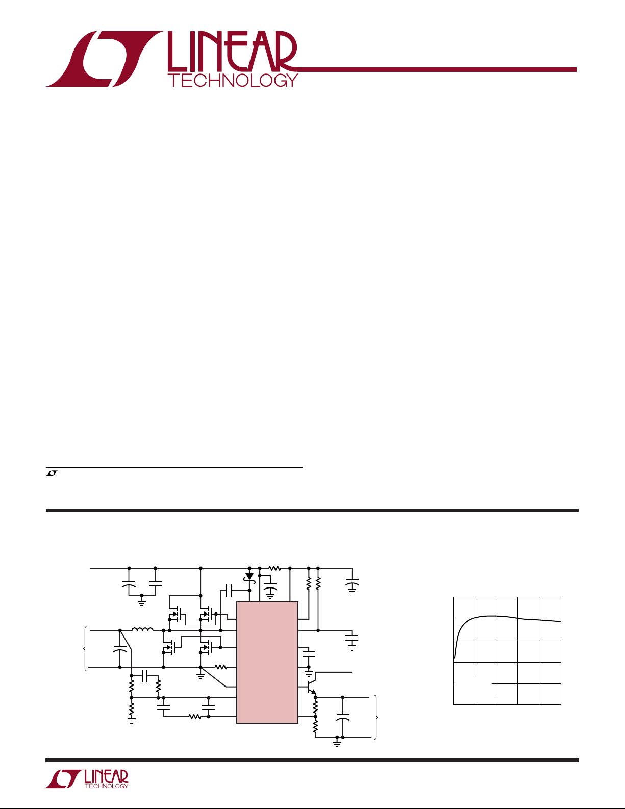
TYPICAL APPLICATIO
5V to 1.8V/15A and 1.5V/2A Application
V
IN
V
OUTSW
1.8V
15A
5V
C
OUTSW
180µF
330µF
10V
4V
×6
C
×3
+
IN
10k
8.06k
+
1µF
QTA
L1
0.68µH
1800pF
C
: KEMET T510X337K010AS
IN
C
OUTSW
L: SUMIDA CEP125-4712-T007
QTA, QTB, QBA, QBB: FAIRCHILD FDS6670A
QTB
QBAQBB
1.8k
1800pF
11k
: PANASONIC EEFUE0G181R
U
MBR0520LT1
C
CP
1µF
14
13.7k
13
330pF
1
2
3
6
5
BOOST
TG
SW
BG
I
MAX
PGND
FB
COMP
16
PV
LTC1704
10Ω
+
15
CC
10µF
V
CC
PGOOD
REGILM
RUN/SS
GND
REGDR
REGFB
5k
11
12
10
4
8
7
9
470k
0.1µF
ON SEMI
D44H11
698Ω
806Ω
+
10µF
1000pF
V
OUTSW
100µF
TANT
1704 TA01
V
OUTREG
1.5V
2A
+
EFFICIENCY (%)
Switcher Efficiency
100
90
80
70
VIN = 5V
60
= 1.8V
V
OUTSW
= 25°C
T
A
QT = QB = 2xFDS6670A
50
3
0
9
12
6
I
(A)
LOAD
15
1704 G04
1704bfa
1
LTC1704/LTC1704B
WW
W
ABSOLUTE AXI U RATI GS
U
UUW
PACKAGE/ORDER I FOR ATIO
(Note 1)
Supply Voltage
VCC, PVCC.............................................................. 6V
BOOST................................................................. 12V
BOOST – SW ......................................................... 6V
Input Voltage
SW ............................................................. –1V to 6V
FB, REGFB, REGILM,
RUN/SS, I
.......................... –0.3V to (VCC + 0.3V)
MAX
Peak Output Current <10µs
TG, BG (Note 7) ..................................................... 5A
Operating Temperature Range (Note 2) .. –40°C to 85°C
Storage Temperature Range ................. –65°C to 150°C
1
TG
2
SW
3
I
MAX
RUN/SS
4
5
COMP
6
FB
7
REGDR
8
GND
16-LEAD PLASTIC SSOP
T
JMAX
TOP VIEW
16
15
14
13
12
11
10
9
GN PACKAGE
= 125°C, θJA = 130°C/W
BOOST
PV
CC
BG
PGND
PGOOD
V
CC
REGILM
REGFB
ORDER PART
NUMBER
LTC1704EGN
LTC1704BEGN
GN PART MARKING
1704
1704B
Lead Temperature (Soldering, 10 sec)..................300°C
Consult LTC Marketing for parts specified with wider operating temperature ranges.
ELECTRICAL CHARACTERISTICS
The ● denotes the specifications which apply over the full operating temperature range, otherwise specifications are at TA = 25°C.
V
= PVCC = BOOST = 5V, unless otherwise specified. (Note 3)
CC
SYMBOL PARAMETER CONDITIONS MIN TYP MAX UNITS
V
CC
PV
BV
I
VCC
I
PVCC
I
BOOST
V
SHDN
I
SS
Switcher Control Loop
V
FB
I
FB
dV
A
FB
GBW Feedback Amplifier Gain Bandwidth Product f = 100kHz (Note 7) 20 MHz
I
COMP
V
PGOOD
I
IMAX
VCC Supply Voltage ● 3.15 5 5.5 V
PVCC Supply Voltage (Note 4) ● 3.15 5 5.5 V
CC
BOOST Pin Voltage V
CC
VCC Supply Current Test Circuit ● 4.5 8 mA
PVCC Supply Current Test Circuit, No Load at Drivers ● 36 mA
BOOST Pin Current Test Circuit ● 26 mA
RUN/SS Shutdown Threshold V
RUN/SS Source Current V
Feedback Voltage ● 0.788 0.800 0.812 V
Feedback Input Current ● ±1 µA
Feedback Voltage Line Regulation VCC = 3.3V to 5.5V ● ±0.01 ±0.1 %/V
FB
Output Voltage Load Regulation (Note 7) ● –0.2 –0.1 %
Feedback Amplifier DC Gain ● 74 85 dB
Feedback Amplifier Output Sink/Source Current ● ±3 ±10 mA
Negative Power Good Threshold ● –15 –10 –6 %
Positive Power Good Threshold ● 61015 %
I
Source Current V
MAX
– VSW (Note 4) ● 3.15 5 5.5 V
BOOST
V
= 0V, V
RUN/SS
= 0V (Notes 5, 6) ● 50 µA
V
RUN/SS
= 0V (Notes 5, 6) ● 50 µA
V
RUN/SS
↑ ● 0.2 0.5 V
RUN/SS
= 0V –3 µA
RUN/SS
= 0V ● –11.5 –10 –8.5 µA
IMAX
= 0V ● 75 150 µA
REGILM
2
1704bfa
LTC1704/LTC1704B
ELECTRICAL CHARACTERISTICS
The ● denotes the specifications which apply over the full operating temperature range, otherwise specifications are at TA = 25°C.
V
= PVCC = BOOST = 5V, unless otherwise specified. (Note 3)
CC
SYMBOL PARAMETER CONDITIONS MIN TYP MAX UNITS
Switcher Switching Characteristics
f
OSC
DC
MAX
t
NOV
tr, t
f
Linear Regulator Controller
V
REGFB
I
REGFB
dV
REGFB
I
REGDR
V
DROPOUT
V
REGILM
I
REGILMINT
V
PGOOD
PGOOD
I
PGOOD
V
OLPG
t
PGOOD
Oscillator Frequency Test Circuit ● 460 550 650 kHz
Maximum Duty Cycle ● 87 90 93 %
Driver Nonoverlap Test Circuit (Note 8) ● 10 25 120 ns
Driver Rise/Fall Time Test Circuit (Note 8) ● 15 100 ns
Feedback Voltage Test Circuit, R
= 680k 0.784 0.800 0.816 V
REGILM
● 0.780 0.800 0.820 V
REGFB Input Current ● ±1 µA
Feedback Voltage Line Regulation Test Circuit, VCC = 4.5V to 5.5V ● ±0.05 ±0.2 %/V
Feedback Voltage Load Regulation Test Circuit, I
= 0mA to 30mA ● –0.2 –0.05 %
REGDR
Driver Output Current Test Circuit ● 30 mA
= 680k, V
R
REGILM
R
= 680k, V
REGILM
Driver Dropout Voltage Test Circuit, I
dV
= –1% (Note 9)
REGFB
REGILM Threshold Test Circuit, R
REGILM Internal Pull-Up Current V
= 0V –1.9 µA
REGILM
REGDR
REGILM
= 0.76V, V
REGFB
= 0V, V
REGFB
= 30mA, V
REGDR
REGDR
= 3.3V 20 mA
REGDR
= 1V 6 mA
= 3.3V, ● 0.65 1.1 V
= 680k 0.8 V
Negative REGFB Power Good Threshold ● –15 –10 –6 %
Positive REGFB Power Good Threshold ● 61015 %
V
Sink Current Power Good ● 10 µA
PGOOD
Power Bad
V
Output Low Voltage I
PGOOD
V
Falling Edge Delay (Note 8) ● 0.5 1 4 µs
PGOOD
V
Rising Edge Delay (Note 8) ● 10 20 40 µs
PGOOD
= 1mA ● 0.03 0.1 V
PGOOD
● 10 mA
Note 1: Absolute Maximum Ratings are those values beyond which the life
of a device may be impaired.
Note 2: The LTC1704E is guaranteed to meet performance specifications
from 0°C to 70°C. Specifications over the –40°C to 85°C operating
temperature range are assured by design, characterization and correlation
with statistical process controls.
Note 3: All currents into device pins are positive; all currents out of device
pins are negative. All voltages are referenced to ground unless otherwise
specified.
Note 4: PV
and BVCC (V
CC
– VSW) must be greater than V
BOOST
GS(ON)
of
the external MOSFETs to ensure proper operation.
Note 5: Supply current in normal operation is dominated by the current
needed to charge and discharge the external MOSFET gates. This current
will vary with supply voltage and the external MOSFETs used.
Note 6: Supply current in shutdown is dominated by external MOSFET
leakage and may be significantly higher than the quiescent current drawn
by the LTC1704, especially at elevated temperature.
Note 7: Guaranteed by design, not subject to test.
Note 8: Rise and fall times are measured using 10% and 90% levels. Delay
and nonoverlap times are measured using 50% levels.
Note 9: Dropout voltage is the minimum V
CC
to V
voltage differential
REGDR
required to maintain regulation at the specified driver output current.
1704bfa
3
LTC1704/LTC1704B
UW
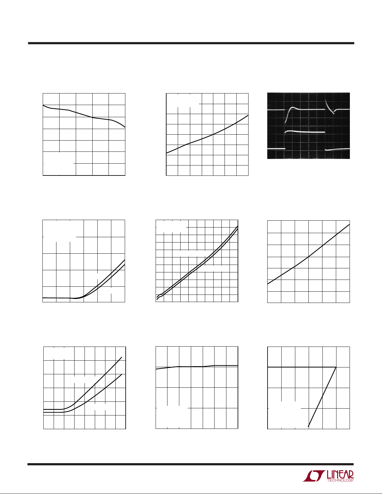
TYPICAL PERFOR A CE CHARACTERISTICS
VFB vs Temperature
0.812
VCC = 5V
0.808
0.804
(V)
0.800
FB
V
0.796
0.792
0.788
–50
–25 0
V
OUTSW
0.6
0
–0.6
(mV)
–1.2
–1.8
OUTSW
∆V
–2.4
–3.0
50 100 125
25 75
TEMPERATURE (°C)
Load Regulation
TA = 25°C
V
OUTSW
1704 G01
= 1.8V
0.03
0
–0.03
–0.07
–0.10
–0.13
–0.17
∆V
OUTSW
(%)
VFB Line Regulation
0.80
TA = 25°C
0.64
0.48
0.32
0.16
(mV)
0
FB
∆V
–0.16
–0.32
–0.48
–0.64
–0.80
3.5
3
4
4.5 5
VCC (V)
Switcher Current Limit Threshold
vs Temperature
24
22
20
18
16
14
CURRENT LIMIT THRESHOLD (A)
12
VIN = 5V
V
OUTSW
∆V
OUTSW
= 13.7k
R
IMAX
QT = QB = 2xFDS6670A
= 1.8V
= –1%
5.5
1704 G02
6
0.10
0.08
0.06
0.04
0.02
0
–0.02
–0.04
–0.06
–0.08
–0.10
FB
∆V
(%)
–3.6
V
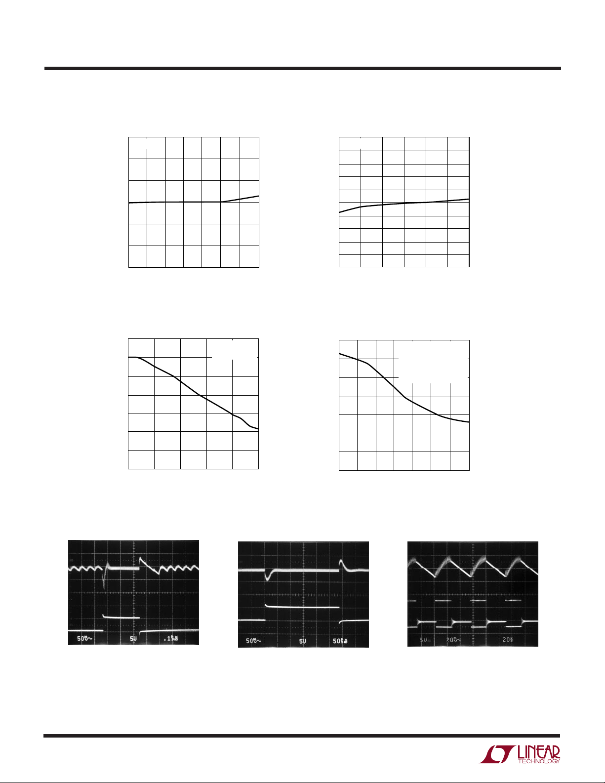
0.5A to 5.5A Load Step
OUTSW
369 15
0
(Burst Mode Operation)
CH1: V
OUTSW
CH2: 0.5A to 5.5A LOAD, 5A DIV
100µs/DIV 1704 G05
= 1.8V, AC 50mV/DIV
I
LOAD
(A)
12
–0.20
1704 G03
V
5A to 10A Load Step
OUTSW
CH1: V
OUTSW
CH2: 5A to 10A LOAD, 5A DIV
50µs/DIV 1704 G06
= 1.8V, AC 50mV/DIV
10
–50
–25 0
TEMPERATURE (°C)
50 100 125
25 75
V
OUTSW
1704 G08
Burst Mode Operation
at 1A Load
CH1: V
CH2: V
OUTSW
TG
20µs/DIV 1704 G07
= 1.8V, AC 20mV/DIV
, 5V DIV
1704bfa
4

UW
TEMPERATURE (°C)
–50
DC
MAX
(%)
91
92
93
25 75
1704 G10
90
89
–25 0
50 100 125
88
87
VCC = 5V
TG, BG FLOAT
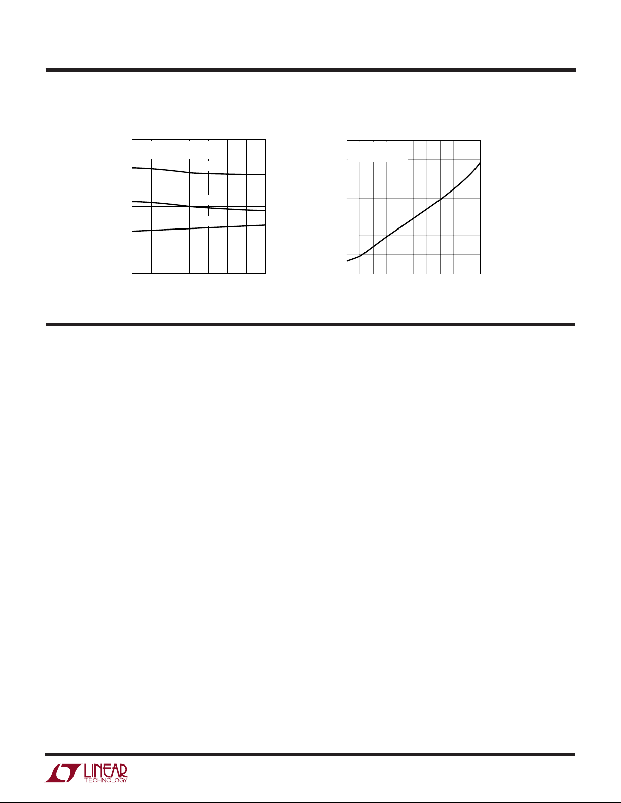
TYPICAL PERFOR A CE CHARACTERISTICS
V
OUTSW
2.0
1.5
(V)
1.0
OUTSW
V
VIN = 5V
0.5
V
OUTSW
T
= 25°C
A
R
IMAX
QT = QB = 2xFDS6670A
0
0
f
OSC
640
VCC = 5V
620
600
580
560
(kHz)
540
OSC
f
520
500
480
460
–25
–50
vs Load Current
= 1.8V
= 13.7k
4
8
LOAD CURRENT (A)
vs Temperature
0
25 125
TEMPERATURE (°C)
50
12
16
75 100
20
1704 G09
1704 G12
(µA)
IMAX
I
–8.5
–9.0
–9.5
–10.0
–10.5
–11.0
–11.5
650
610
570
(kHz)
OSC
f
530
490
450
I
vs Temperature I
IMAX
VCC = 5V
50 100 125
–50
f
3
OSC
–25 0
vs V
TA = 25°C
3.5
25 75
TEMPERATURE (°C)
CC
4 4.5 5
VCC (V)
1704 G10
5.5 6
1704 G13
LTC1704/LTC1704B
vs V
IMAX
–8.5
TA = 25°C
–9.0
–9.5
(µA)
–10.0
IMAX
I
–10.5
–11.0
–11.5
3
Maximum TG Duty Cycle
vs Temperature
3.5
CC
4 4.5 5
VCC (V)
5.5 6
1704 G11
Drivers Rise and Fall Time
vs Load
100
TA = 25°C
90
PV
= BOOST = 5V
CC
80
70
60
(ns)
f
50
, t
r
t
40
30
20
10
0
2000
0
4000
TG, BG LOAD (pF)
6000
8000
10000
1704 G15
0.820
0.815
0.810
0.805
(V)
0.800
REGFB
V
0.795
0.790
0.785
0.780
V
vs Temperature
REGFB
V
= 3.3V
REGDR
–25 0 50
–50
25
TEMPERATURE (°C)
75 100 125
LTXXX • TPCXX
1.6
1.2
0.8
0.4
(mV)
REGFB
–0.4
∆V
–0.8
–1.2
–1.6
V
Line Regulation
REGFB
TA = 25°C
= 0.8V
V
REGDR
0
3.5 4 5
3
4.5
VCC (V)
5.5
1704 G17
6
0.20
0.15
0.10
0.05
0
–0.05
–0.10
–0.15
–0.20
1704bfa
5
∆V
REGFB
(%)
LTC1704/LTC1704B
I
REGILM
(µA)
0
35
30
25
20
15
10
5
0
610
1704 G23
24
812
I
REGDR
(mA)
I
OUTREG
(A)
0
0
V
OUTREG
(V)
0.5
1.0
1.5
2.0
0.5 1 1.5 2
1704 G25
2.5 3
TA = 25°C
V
INREG
= 1.8V
V
OUTREG
= 1.5V
I
REGILM
= 9µA
QEXT = D44H11
UW
TYPICAL PERFOR A CE CHARACTERISTICS
Linear Regulator Dropout Voltage
V
0.5
0
–0.5
(mV)
–1.0
–1.5
OUTREG
∆V
–2.0
–2.5
–3.0
0
Minimum VCC vs V
5.5
5.0
(V)
4.5
CC
4.0
MINIMUM V
3.5
3.0
0.9
Load Regulation
OUTREG
TA = 25°C
= 1.5V
V
OUTREG
I
= 9µA
REGILM
QEXT = D44H11
0.4 0.8 1.2 2
I
(A)
OUTREG
OUTREG
I
= 9µA
REGILM
= 2A
I
OUTREG
= –1%
∆V
OUTREG
QEXT = D44H11
TA = –40°C
1.7 2.1 2.5
1.3
V
(V)
OUTREG
T
A
1.6
= 25°C
1704 G18
2.9 3.3
1704 G21
0.03
0
–0.03
–0.07
–0.10
–0.13
–0.17
–0.20
vs Temperature
1.1
I
= –30mA
REGDR
= 3.3V
V
REGDR
1.0
0.9
∆V
0.8
OUTREG
(V)
0.7
(%)
DROPOUT
V
0.6
0.5
0.4
0.3
–25 0 50
–50
TEMPERATURE (°C)
Linear Regulator Start-Up Time
vs C
0
0
DELAY
TA = 25°C
V
OUTREG
2000
= 1.5V
I
REGILM
4000
C
DELAY
= 6.2µA
(pF)
1100
1000
900
800
700
600
500
400
START-UP TIME (µs)
300
200
100
25
6000
I
REGILM
= 9µA
8000
75 100 125
1704 G19
10000
1704 G22
V
V
OUT
I
LOAD
CH1: V
CH2: 0.1A to 2.1A LOAD, 1A DIV
I
0.1A to 2.1A Load Step
OUTREG
= 1.5V, AC 50mV/DIV
OUTREG
vs I
REGDR
REGILM
50µs/DIV 1704 G20
30
25
20
(mA)
15
REGDR
I
10
5
0
6
I
vs V
REGDR
TA = 25°C
V
REGDR
0
REGFB
= 0V
I
REGILM
0.1 0.3
0.2 0.4
V
REGFB
= 9µA
I
REGILM
0.5
(V)
= 6.2µA
0.6
0.7
1704 G28
0.8
Linear Regulator Current Limit
Threshold vs Temperature
3.0
2.5
2.0
1.5
V
= 1.8V
INREG
= 1.5V
V
OUTREG
CURRENT LIMIT THRESHOLD (A)
1.0
–50
= 9µA
I
REGILM
QEXT = D44H11
–25 0 25 50
TEMPERATURE (°C)
75 100 125
1704 G24
V
OUTREG
vs Load Current
1704bfa
UW
TYPICAL PERFOR A CE CHARACTERISTICS
LTC1704/LTC1704B
Supply Current vs Temperature I
6.0
VCC = PVCC = BOOST = 5V
TG, BG FLOAT
I
4.5
3.0
SUPPLY CURRENT (mA)
1.5
0
–50
–25 0 25 50
TEMPERATURE (°C)
VCC
I
PVCC
I
BOOST
75 100 125
1704 G26
UUU
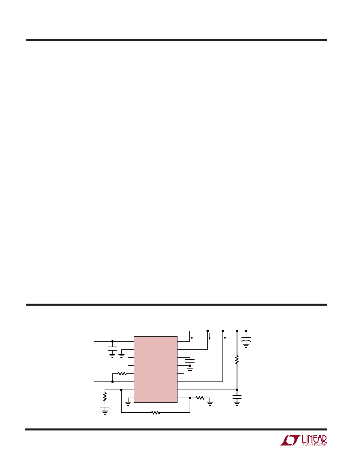
PI FU CTIO S
TG (Pin 1): Switcher Controller Top Gate Drive. The TG pin
drives the gate of the top N-channel MOSFET, QT. The TG
driver draws power from the BOOST pin and returns it to
the SW pin, providing true floating drive to QT. TG is designed to typically drive up to 10,000pF of gate capacitance.
SW (Pin 2): Switcher Controller Switching Node. Connect
SW to the switching node of the main converter. The TG
driver ground returns to SW, providing floating gate drive
to the top N-channel MOSFET, QT. The voltage at SW is
compared to I
the bottom MOSFET, QB is on. The Burst comparator
(BURST, see Block Diagram) monitors the potential at SW
and switches to Burst Mode operation under light load
conditions.
I
(Pin 3): Switcher Controller Current Limit Set. The
MAX
I
pin sets the current limit comparator threshold for
MAX
the switcher controller. If the voltage drop across the
bottom MOSFET, QB, exceeds the magnitude of the voltage at I
The I
MAX
pin has an internal 10µA current source pull-up,
MAX
allowing the current threshold to be set with a single
external resistor to PGND. Kelvin connect this current
setting resistor to the source of QB. Refer to the Current
Limit Programming section for more information on choosing R
IMAX
.
by the current limit comparator while
MAX
, the switcher controller enters current limit.
35
30
25
(mA)
20
BOOST
, I
15
PVCC
I
10
PVCC
TA = 25°C
PV
5
0
0
, I
= BOOST = 5V
CC
2000
vs Driver Load
BOOST
4000
TG, BG LOAD (pF)
6000 8000
10000
1704 G27
RUN/SS (Pin 4): Switcher Controller Soft-Start. A capacitor from RUN/SS to GND controls the turn-on time and
rate of rise of the switcher output voltage at power up. An
internal 3µA current source pull-up at RUN/SS sets the
turn-on time at approximately 300ms/µF. If both RUN/SS
and REGILM are pulled low, the LTC1704 enters shutdown
mode.
COMP (Pin 5): Switcher Controller Loop Compensation.
The COMP pin is connected directly to the output of the
switcher controller’s error amplifier and the input to the
PWM comparator. Use an RC network between the COMP
pin and the FB pin to compensate the feedback loop for
optimum transient response.
FB (Pin 6): Switcher Controller Feedback Input. FB should
be connected through a resistor divider network to V
OUTSW
to set the switcher output voltage. Also, connect the
switcher loop compensation network to FB.
REGDR (Pin 7): Linear Regulator Controller Driver Output.
Connect REGDR to the base of the external NPN Pass
transistor. The REGILM pin input current controls the
linear regulator controller maximum driving capability.
GND (Pin 8): Signal Ground. All internal low power circuitry returns to the GND pin. Connect to a low impedance
ground, separated from the PGND node. All feedback,
1704bfa
7
LTC1704/LTC1704B
UUU
PI FU CTIO S
compensation and soft-start connections should return to
GND. GND and PGND should connect only at a single
point, near the PGND pin and the negative plate of the V
IN
bypass capacitor.
REGFB (Pin 9): Linear Regulator Controller Feedback
Input. REGFB should be connected through a resistor
divider network to V
OUTREG
to set the output voltage of the
linear regulator.
REGILM (Pin 10): Linear Regulator Controller Current
Limit Setting cum ON/OFF Control. This pin is internally
servoed to 0.8V. An external resistor R
REGILM
between V
CC
and REGILM programs the REGILM pin input current. This
current determines the maximum pass transistor base
current and directly controls the linear regulator current
sourcing capabilitiy. An external capacitor, C
DELAY
is added
to this pin to control the turn-on time of the linear regulator, the minimum value for this capacitor is 100pF. Refer
to the Linear Regulator Current Limit Programming section for more information on choosing R
REGILM
and C
DELAY
.
Pulling REGILM to GND turns off the linear regulator. If
both RUN/SS and REGILM are pulled low, the LTC1704
enters shutdown mode.
VCC (Pin 11): Power Supply Input. All internal circuits
except the switcher output drivers are powered from this
pin. VCC should be connected to a low noise 5V supply, and
should be bypassed to GND with at least a 10µF capacitor
in close proximity to the LTC1704.
PGOOD (Pin 12): Power Good. PGOOD is an open-drain
logic output. PGOOD pulls low if any of the two supply
outputs are outside ±10% of their nominal levels. An
external pull-up resistor is required at PGOOD to allow it
to swing positive.
PGND (Pin 13): Power Ground. The BG driver returns to
this pin. Connect PGND to a high current ground node in
close proximity to the sources of external MOSFET QB,
and the VIN and V
bypass capacitors.
OUTSW
BG (Pin 14): Switcher Controller Bottom Gate Drive. The
BG pin drives the gate of the bottom N-channel synchronous switch MOSFET, QB. BG is designed to typically drive
up to 10,000pF of gate capacitance.
PVCC (Pin 15): Switcher Controller Bottom Gate Driver Supply. PVCC provides power to the BG output driver. PV
CC
must be connected to a voltage high enough to fully turn
on the external MOSFET, QB. PV
nected directly to VIN, the main system 5V supply. PV
should generally be con-
CC
CC
requires at least a 10µF bypass capacitor directly to PGND.
BOOST (Pin 16): Switcher Controller Top Gate Driver
Supply. The BOOST pin supplies power to the floating TG
driver. Bypass BOOST to SW with a 1µF capacitor. An
external Schottky diode from VIN to BOOST creates a
complete floating charge-pumped supply at BOOST. No
other external supplies are required.
TEST CIRCUIT
8
BOOST
2000pF
80k
I
PVCCIVCC
1
f
OSC
2000pF
V
FB
100Ω
1µF
TG
2
SW
3
I
MAX
4
RUN/SS
2k
5
COMP
6
FB
7
REGDR
8
GND
LTC1704
250k
BOOST
PV
BG
PGND
PGOOD
V
REGILM
REGFB
CC
CC
I
16
15
14
13
12
11
10
9
+
R
REGILM
100k
100pF
1704 TC
5V
10µF
1704bfa
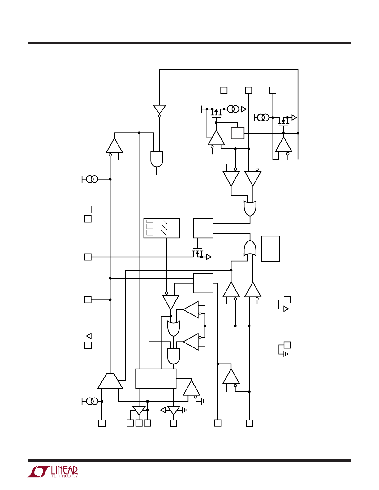
BLOCK DIAGRA
PWRGD
DELAY
OSC
550kHz
0.720V
0.8V
0.8V
POWER-UP LINEAR REGULATOR
REGFB
0.880V
SOFT-
START
BURST
AND
DRIVER
LOGIC
0.720V
0.880V
0.760V0.840V
0.800V
MPG
PWRBAD
REG
PWRBAD
SWITCHER
0.5V
POWER
DOWN
SHUTDOWN
SWITCHER DRIVER
10µA
MAX
BURST
MIN
PPGREG
NPGREG
PPG
NPG
SSCMP
PWM
ILM
I
MAX
BOOST
PGOODRUN/SS
TG
SW
COMP
FB
1704 BD
PV
CC
PGND
GND
V
CC
3µA
15
11
4
12
8
13
6
5
2
BG
PV
CC
14
1
16
3
0.8V
BANDGAP
REFERENCE
REG
ILM
2mA
REGDR
MREG
1.9µA
7
REGFB
9
REGILM
MREGILM
AMP
FB
10
V
B
= 2V TYP
V
A
= 1V TYP
W
LTC1704/LTC1704B
1704bfa
9

LTC1704/LTC1704B
U
WUU
APPLICATIO S I FOR ATIO
OVERVIEW
The LTC1704 includes a step-down (buck), voltage mode
feedback switching regulator controller and a linear regulator controller. The switching regulator controller employs a synchronous switching architecture with two
external N-channel MOSFETs. The chip operates from a
low voltage input supply (6V maximum) and provides high
power, high efficiency, precisely regulated output voltage.
The switcher output regulation is extremely tight, with
initial accuracy and DC line and load regulation and better
than 1.5%. Total regulation, including transient response,
is inside of 3.5% with a properly designed circuit. The
550kHz switching frequency allows the use of physically
small, low value external components without compromising performance.
The LTC1704’s internal feedback amplifier is a 20MHz gain
bandwidth op amp, allowing the use of complex multipole/
zero compensation networks. This allows the feedback
loop to maintain acceptable phase margin at higher frequencies than traditional switching regulator controllers,
improving stability and maximizing transient response.
The 800mV internal reference allows regulated output
voltages as low as 800mV without external level shifting
amplifiers. The LTC1704’s synchronous switching logic
transitions automatically into Burst Mode operation, maximizing efficiency with light loads.
The linear regulator controller drives an external NPN pass
transistor to provide a programmable output voltage up to
2A of current. An external pull-up resistor programs the
current limit threshold for the linear regulator. Under
short-circuit condition, the foldback current limit circuitry
prevents excessive pass transistor heating. The switcher
and the linear regulator can be individually disabled. When
both controllers are disabled, the LTC1704 enters shutdown mode and the supply current reduces to 75µA. An
onboard power good (PGOOD) flag goes high when both
outputs are regulating.
Small Footprint
The LTC1704 switcher supply operates at a 550kHz switching frequency, allowing it to use low value inductors
without generating excessive ripple currents. Because the
inductor stores less energy per cycle, the physical size of
the inductor can be reduced without risking core saturation, saving PCB board space. The high operating frequency also means less energy is stored in the output
capacitors between cycles, minimizing their required value
and size. The remaining components, including the
LTC1704, are tiny, allowing an entire power convertor to
be constructed in 1.5in2 of PCB space.
Fast Transient Response
The LTC1704 switcher supply uses a fast 20MHz GBW op
amp as an error amplifier. This allows the compensation
network to be designed with several poles and zeros in a
more flexible configuration than with a typical gm feedback
amplifier. The high bandwidth of the amplifier, coupled
with the high switching frequency and the low values of the
external inductor and output capacitor, allow very high
loop crossover frequencies. The low inductor value is the
other half of the equation—with a typical value on the
order of 1µH, the inductor allows very fast di/dt slew rates.
The result is superior transient response compared with
conventional solutions.
High Efficiency
The LTC1704 switcher supply uses a synchronous stepdown (buck) architecture, with two external N-channel
MOSFETs. A floating topside driver and a simple external
charge pump provide full gate drive to the upper MOSFET.
The voltage mode feedback loop and MOSFET VDS current
limit sensing remove the need for an external current
sense resistor, eliminating an external component and a
source of power loss in the high current path. Properly
designed circuits using low gate charge MOSFETs are
capable of efficiencies exceeding 90% over a wide range
of output voltages.
Linear Regulator Controller
The LTC1704 linear regulator controller drives an external NPN pass transistor in emitter-follower configuration
to provide an externally adjustable output voltage. The controller senses the output voltage via the REGFB pin, drives
the base of the NPN through the REGDR pin to regulate
the REGFB pin to 0.8V. REGDR is capable of sourcing more
than 30mA of base current to the external NPN.
1704bfa
10

LTC1704/LTC1704B
TG
C
CP
D
CP
BOOST
SW
BG
PGND
PV
CC
LTC1704
QT
C
IN
QB
L
+
C
OUTSW
1704 F02
V
OUTSW
V
IN
+
U
WUU
APPLICATIO S I FOR ATIO
Overcurrent protection is achieved by limiting the drive
current. The input current at the REGILM pin programs the
current limit threshold. Refer to the Linear Regulator
Supply Current Limit Programming section for more
information on choosing R
REGILM
controller employs a foldback current limit scheme for
overcurrent protection. Under a short-circuit condition,
the external NPN transistor is subjected to the full input
voltage across its collector-emitter terminal. This increases
the power dissipation of the NPN and may eventually
cause damage to the transistor. LTC1704 overcomes this
problem by using a foldback current limit scheme whereby
the available drive current is reduced as the output voltage
at REGFB pin drops. This limits the power dissipation and
prevents catastrophic damage to the external NPN.
ARCHITECTURE DETAILS
Switcher Supply Architecture
The LTC1704 switcher supply is designed to operate as a
synchronous buck converter (Figure 1). The controller
includes two high power MOSFET gate drivers to control
the external N-channel MOSFETs QT and QB. The drivers
have 0.5Ω output impedances and can carry over an amp
of continuous current with peak currents up to 5A to slew
large MOSFET gates quickly. The drain of QT is connected
to the input supply and the source of QT connected to the
switching node SW. QB is the synchronous rectifier with
its drain at SW and its source at PGND. SW is connected
to one end of the inductor, with the other end connected
to V
. The output capacitor is connected from V
OUTSW
to PGND.
. The linear regulator
OUTSW
When a switching cycle begins, QB is turned off and QT is
turned on. SW rises almost immediately to VIN and the
inductor current begins to increase. When the PWM pulse
completes, QT turns off and one nonoverlap interval later,
QB turns on. Now SW drops to PGND and the inductor
current decreases. The cycle repeats with the next tick of
the master clock. The percentage of time spent in each
mode is controlled by the duty cycle of the PWM signal,
which in turn is controlled by the feedback amplifier. The
master clock runs at a 550kHz rate and turns QT once
every 1.8µs. In a typical application with a 5V input and a
1.5V output, the duty cycle will be set at 1.5/5 • 100% or
30% by the feedback loop. This will give roughly a 540ns
on-time for QT and a 1.26µs on-time for QB.
This constant frequency operation brings with it a couple
of benefits. Inductor and capacitor values can be chosen
with a precise operating frequency in mind and the feedback loop components can be similarly tightly specified.
Noise generated by the circuit will always be in a known
frequency band with the 550kHz frequency designed to
leave the 455kHz IF band free of interference. Subharmonic
oscillation and slope compensation, common headaches
with constant frequency current mode switchers, are
absent in voltage mode designs like the LTC1704. During
the time that QT is on, its source (the SW pin) is at VIN. V
IN
is also the power supply for the LTC1704. However, QT
requires VIN + V
at its gate to achieve minimum RON.
GS(ON)
The LTC1704, needs to generate a gate drive signal at TG
higher than its highest supply voltage. To accomplish this,
the TG driver runs from floating supplies, with its negative
supply attached to SW and its power supply at BOOST.
This allows it to slew up and down with the source of QT.
V
IN
+
C
+
1704 F01
IN
V
OUTSW
C
OUTSW
Figure 2. Floating TG Driver Supply
1704bfa
TG
SW
LTC1704
BG
PGND
Figure 1. Synchronous Buck Architecture
QT
QB
L
11

LTC1704/LTC1704B
U
WUU
APPLICATIO S I FOR ATIO
In combination with a simple external charge pump (Figure 2), this allows the LTC1704 to completely enhance the
gate of QT without requiring an additional, higher supply
voltage.
Switcher Supply Feedback Amplifier
The LTC1704 senses the switcher output voltage at V
with an internal feedback op amp (see Block Diagram).
This is a real op amp with a low impedance output, 85dB
open-loop gain and 20MHz gain bandwidth product. The
positive input is connected internally to an 800mV reference, while the negative input is connected to the FB pin.
The output is connected to COMP, which is in turn connected to the soft-start circuitry and from there to the
PWM generator. The switching regulator output voltage
can be obtained using the following equation:
R
1
VV
OUTSW
=+
08 1
.•
R
2
Unlike many regulators that use a resistor divider connected to a high impedance feedback input, the LTC1704
switcher supply is designed to use an inverting summing
amplifier topology with the FB pin configured as a virtual
ground. This allows flexibility in choosing pole and zero
locations not available with simple gm configurations. In
particular, it allows the use of “Type 3” compensation,
which provides a phase boost at the LC pole frequency
and significantly improves loop phase margin (refer to
Figure␣ 3).
C3
+
COMP
LTC1704
R4
FB
C2
Figure 3. "Type 3" Feedback Loop
0.8V
FB
–
C1
R3
R1
R2
1704 F03
V
OUTSW
OUTSW
Switcher Supply MIN/MAX Comparators
Two additional feedback loops in the switcher supply keep
an eye on the primary feedback amplifier and step in if the
feedback node moves ±5% from its nominal 800mV value.
The MAX comparator (see Block Diagram) activates whenever FB rises more than 5% above 800mV. It immediately
turns the top MOSFET (QT) off and the bottom MOSFET
(QB) on and keeps them that way until FB falls back within
5% of its nominal value. This pulls the output down as fast
as possible, preventing damage to the (often expensive)
load. If FB rises because the output is shorted to a higher
supply, QB will stay on until the short goes away, the
higher supply current limits or QB dies trying to save the
load. This behavior provides maximum protection against
overvoltage faults at the output, while allowing the circuit
to resume normal operation when the fault is removed.
The MIN comparator (see Block Diagram) trips whenever
FB is more than 5% below 800mV and immediately forces
the switch duty cycle to 90% to bring the output voltage
back into range. It releases when FB is within the 5%
window. MIN is disabled when the soft-start or current
limit circuits are active—the only two times that the output
should legitimately be below its regulated value.
Notice that the FB pin is the virtual ground node of the
feedback amplifier. A typical compensation network does
not include local DC feedback around the amplifier, so that
the DC level at FB will be an accurate replica of the output
voltage, divided down by R1 and R2 (Figure 3). However,
the compensation capacitors will tend to attenuate AC
signals at FB, especially with low bandwidth Type 1 feedback loops. This creates a situation where the MIN and
MAX comparators do not respond immediately to shifts in
the output voltage, since they monitor the output at FB.
PGOOD Flag
The LTC1704 comes with a power good pin (PGOOD).
PGOOD is an open-drain output, and requires an external
pull-up resistor. If both the regulators are within ±10%
from their nominal value, the transistor MPG shuts off (see
Block Diagram), and PGOOD is pulled high by the external
pull-up resistor. If any of the two outputs is more than 10%
outside the nominal value for more than 1µs, PGOOD pulls
12
1704bfa

LTC1704/LTC1704B
U
WUU
APPLICATIO S I FOR ATIO
low, indicating that the output is out of regulation. For
PGOOD to go high, both the outputs must be in regulation
for more than 20µs. PGOOD remains active during soft-
start and current limit. Upon power-up, PGOOD is forced
low. As soon as the RUN/SS and REGILM pins rise above
the shutdown thresholds, the two pairs of power good
comparators take over and control the transistor MPG
directly. The 1µs and 20µs delay ensures that short output
transient glitches that are successfully “caught” by the
power good comparators don’t cause momentary glitches
at the PGOOD pin.
Shutdown/Soft-Start
The RUN/SS pin performs two functions: when pulled to
ground, it shuts down the switcher drivers, and acts as a
conventional soft-start pin, enforcing a maximum duty
cycle limit proportional to the voltage at RUN/SS. An
internal 3µA current source pull-up is connected to the
RUN/SS pin, allowing a soft-start ramp to be generated
with a single external capacitor to ground. The 3µA current
source is active even when the LTC1704 is shut down,
ensuring the device will start when any external pull-down
at RUN/SS is released.
The RUN/SS pin shuts down the switcher drivers when it
falls below 0.5V (Figure 4). Between 0.5V and about 1V,
the LTC1704 wakes up and the duty cycle is kept to
minimum. As the potential at RUN/SS goes higher, the
duty cycle increases linearly between 1V and 2V, reaching
its final value of 90% when RUN/SS is above 2V. Somewhere before this point, the feedback amplifier will assume control of the loop and the output will come into
regulation. When RUN/SS rises to 1V below VCC , the MIN
feedback comparator is enabled, and the LTC1704 voltage
feedback loop is in full operation.
Switcher Supply Current Limit
The LTC1704 switcher supply includes an onboard current limit circuit that limits the maximum output current to
a user-programmed level. It works by sensing the voltage
drop across QB during the time that QB is on and comparing that voltage to a user-programmed voltage at I
Since QB looks like a low value resistor during its on-time,
the voltage drop across it is proportional to the current
MAX
.
flowing in it. In a buck converter, the average current in the
inductor is equal to the output current. This current also
flows through QB during its on-time. Thus, by watching
the voltage across QB, the LTC1704 can monitor the
output current.
Any time QB is on and the current flowing to the output is
reasonably large, the SW node at the drain of QB will be
somewhat negative with respect to PGND. The LTC1704
senses this voltage and inverts it to allow it to compare the
sensed voltage with a positive voltage at the I
I
pin includes a trimmed 10µA pull-up, enabling the
MAX
user to set the voltage at I
with a single resistor, R
MAX
MAX
pin. The
IMAX
,
to ground. The LTC1704 compares the two inputs and
begins limiting the output current when the magnitude of
the negative voltage at the SW pin is greater than the
voltage at I
MAX
.
The current limit detector is connected to an internal gm
amplifier that pulls a current from the RUN/SS pin proportional to the difference in voltage magnitudes between the
SW and I
pins. This current begins to discharge the
MAX
soft-start capacitor at RUN/SS, reducing the duty cycle
and controlling the output voltage until the current drops
below the limit. The soft-start capacitor needs to move a
fair amount before it has any effect on the duty cycle,
adding a delay until the current limit takes effect (Figure 4).
This allows the LTC1704 to experience brief overload
conditions without affecting the output voltage regulation.
V
OUT
CURRENT
0V
5V
4V
2V
1V
0.5V
0V
Figure 4. Soft-Start Operation in Start Up and Current Limit
START-UP
MINIMUM DUTY CYCLE
DRIVER DISABLE MODE
LTC1704 ENABLE
OPERATION
COMP CONTROLS
DUTY CYCLE
RUN/SS CONTROLS
DUTY CYCLE
LIMIT
NORMAL
COMPARATOR
ENABLE
MIN
HARD
CURRENT
LIMIT
1704 F04
1704bfa
13

LTC1704/LTC1704B
U
WUU
APPLICATIO S I FOR ATIO
The delay also acts as a pole in the current limit loop to
enhance loop stability. Prolonged overload conditions will
allow the RUN/SS pin to reach a steady state, and the
output will remain at a reduced voltage until the overload
is removed. Under current limit condition, if the output
voltage is less than 10% of its normal value, the soft-start
capacitor will be forced low immediately and the LTC1704
will rerun a complete soft-start cycle. The soft-start capacitor must be selected such that during power-up the
current through QB will not exceed the current limit value.
Power MOSFET R
limiting the accuracy obtainable from the LTC1704 current
limit loop. Additionally, ringing on the SW node due to
parasitics can add to the apparent current, causing the
loop to engage early. When the load current increases
abruptly, the voltage feedback loop forces the duty cycle
to increase rapidly and the on-time of QB will be small
momentarily. The R
ensure that the SW node is pulled low within the QB ontime for proper current sensing. The LTC1704 current limit
is designed primarily as a disaster prevention, “no blowup” circuit, and is not useful as a precision current regulator. It should typically be set around 50% above the
maximum expected normal output current to prevent component tolerances from encroaching on the normal current range. See the Switching Supply Current Limit Programming section for advice on choosing a valve for R
varies from MOSFET to MOSFET,
DS(ON)
of QB must be low enough to
DS(ON)
IMAX
.
Continuous mode works efficiently when the load current
is greater than half of the ripple current in the inductor. In
a buck converter like the LTC1704, the average current in
the inductor (averaged over one switching cycle) is equal
to the load current. The ripple current is the difference
between the maximum and the minimum current during
a switching cycle (see Figure 5a). The ripple current
depends on inductor value, clock frequency and output
voltage, but is constant regardless of load as long as the
LTC1704 remains in Continuous mode. See the Inductor
Selection section for a detailed description of ripple
current.
As the output load current decreases in Continuous mode,
the average current in the inductor will reach a point where
it drops below half the ripple current. At this point, the
current in the inductor will reverse during a portion of the
switching cycle, or begin to flow from the output back to
the input. This does not adversely affect regulation, but
does cause additional losses as a portion of the inductor
current flows back and forth through the resistive power
switches, giving away a little more power each time and
lowering the efficiency. There are some benefits to allowing this reverse current flow: the circuit will maintain
regulation even if the load current drops below zero (the
load supplies current to the LTC1704) and the output
ripple voltage and frequency remain constant at all loads,
easing filtering requirements.
BURST MODE OPERATION
Theory of Operation
The LTC1704 (non-B part) switcher supply has two modes
of operation. Under heavy loads, it operates as a fully
synchronous, continuous conduction switching regulator. In this mode of operation (“Continuous” mode), the
current in the inductor flows in the positive direction
(toward the output) during the entire switching cycle,
constantly supplying current to the load. In this mode, the
synchronous switch (QB) is on whenever QT is off, so the
current always flows through a low impedance switch,
minimizing voltage drop and power loss. This is the most
efficient mode of operation at heavy loads, where the
resistive losses in the power devices are the dominant loss
term.
(For Non-B Parts Only)
14
Besides the reverse current loss, the LTC1704 drivers are
still switching QT and QB on and off once a cycle. Each time
an external MOSFET is turned on, the internal driver must
charge its gate to PVCC. Each time it is turned off, that
charge is lost to ground. At the high switching frequency
that the LTC1704 operates, the charge lost to the gates can
add up to tens of milliamps from PVCC. As the load current
continues to drop, this quickly becomes the dominant
power loss term, reducing efficiency once again.
To minimize the efficiency loss due to switching loss and
reverse current flow at light loads, the LTC1704 (non-B
part) switches to a second mode of operation: Burst Mode
operation (Figure 5b). In Burst Mode operation, the
LTC1704 detects when the inductor current approaches
zero and turns off both drivers. During this time, the
voltage at the SW pin will float around V
OUTSW
, the voltage
1704bfa

LTC1704/LTC1704B
U
WUU
APPLICATIO S I FOR ATIO
across the inductor will be zero, and the inductor current
remains zero. This prevents current from flowing backwards in QB, eliminating that power loss term. It also
reduces the ripple current in the inductor as the output
current approaches zero.
I
RIPPLE
I
AVERAGE
INDUCTOR CURRENT
Figure 5a. Continous Mode
INDUCTOR CURRENT
Figure 5b. Burst Mode Operation
I
RIPPLE
TIME
TIME
I
AVERAGE
1704 F05
The burst comparator is turned on only at the last 180ns
of the switching period, the propagation delay of the
comparator is designed to be fast so that a zero or low
positive voltage on the SW node can trip the comparator
within this 180ns. Low inductor ripple current coupled
with low MOSFET R
may prolong the delay of the
DS(ON)
burst comparator and prevent the comparator from tripping. To overcome this, reduce the inductor value to
increase the ripple current and the SW node voltage
change.
The moment LTC1704 (non-B parts) enters Burst Mode
operation, both drivers skip several switching cycles until
the output droops. Once the voltage feedback loop requests
for an additional 10% duty cycle, the LTC1704 enters Continuous mode operation again. To eliminate audible noise
from certain types of inductors when they are lightly loaded,
LTC1704 includes an internal timer that forces Continuous
mode operation every 15µs.
The LTC1704B does not shift into Burst Mode operation at
light loads, eliminating low frequency output ripple at the
expense of light load efficiency.
The LTC1704 detects when the inductor current has
reached zero by monitoring the voltage at the SW pin while
QB is on (see BURST in Block Diagram). Since QB acts like
a resistor, SW should ideally be right at 0V when the
inductor current reaches zero. In reality, the SW node will
ring to some degree immediately after it is switched to
ground by QB, causing some uncertainty as to the actual
moment the average current in QB goes to zero. The
LTC1704 minimizes this effect by turning on the Burst
Comparator only at the last 180ns of the switching period,
before QB turns off. In addition, the Burst Comparator is
disabled if QB turns on for less than 200ns. Despite this,
care must still be taken in the PCB layout to ensure that
proper kelvin sensing for the SW pin is provided. Connect
the SW pin of the LTC1704 as close to the drain of QB as
possible through a thick trace. The same applies to the
PGND pin of the LTC1704, which is the negative input of
the burst comparator and it should be connected close to
the source of QB through a thick trace. Ringing on the
PGND pin due to an insufficient PVCC bypass capacitor can
also cause the burst comparator to trip prematurely.
Connect at least a 10µF bypass capacitor directly from the
PVCC pin to PGND.
In Burst Mode operation, both resistive loss and switching
loss are minimized while keeping the output in regulation.
The total deviation from the regulated output is within the
1.5% regulation tolerance of the LTC1704. As the load
current falls to zero in Burst Mode operation, the most
significant loss term becomes the 4.5mA quiescent current drawn by the LTC1704—usually much less than the
minimum load current in a typical low voltage logic system. Burst Mode operation maximizes efficiency at low load
currents, but can cause low frequency ripple in the output
voltage as the cycle-skipping circuitry switches on and off.
V
SW
0V
5V
V
BG
0V
BURST
COMPARATOR
DISABLED IF QB
TURNS ON FOR
LESS THAN 200ns
Figure 6. Burst Comparator Turns On 180ns Before QB Turns Off
BURST
COMPARATOR
TURNS ON
180ns BEFORE
QB TURNS OFF
TIME
TIME
1704 F06
1704bfa
15

LTC1704/LTC1704B
U
WUU
APPLICATIO S I FOR ATIO
Maximizing High Load Current Efficiency
Efficiency at high load currents is primarily controlled by
the resistance of the components in the power path (QT,
QB, L) and power lost in the gate drive circuits due to
MOSFET gate charge. Maximizing efficiency in this region
of operation is as simple as minimizing these terms.
The behavior of the load over time affects the efficiency
strategy. Parasitic resistances in the MOSFETs and the
inductor set the maximum output current the circuit can
supply without burning up. A typical efficiency curve
shows that peak efficiency occurs near 30% of this maximum current. If the load current will vary around the
efficiency peak and spend relatively little time at the
maximum load, choosing components so that the average
load is at the efficiency peak is a good idea. This puts the
maximum load well beyond the efficiency peak, but usually gives the greatest system efficiency over time, which
translates to the longest run time in a battery-powered
system. If the load is expected to be relatively constant at
the maximum level, the components should be chosen so
that this load lands at the peak efficiency point, well below
the maximum possible output of the converter.
Maximizing Low Load Current Efficiency
Low load current efficiency depends strongly on proper
operation in Burst Mode operation. In an ideally optimized
system, when Burst Mode operation is activated, gate
drive is the dominant loss term. Burst Mode operation
turns off all output switching for several clock cycles in a
row, significantly cutting gate drive losses. As the load
current in Burst Mode operation falls toward zero, the
current drawn by the circuit falls to the LTC1704’s background quiescent level, about 4.5mA.
To maximize low load efficiency, make sure the LTC1704
(non-B part) is allowed to enter Burst Mode operation as
cleanly as possible. Minimize ringing at the SW node so
that the Burst comparator leaves as little residual current
in the inductor as possible when QB turns off. It helps to
connect the SW pin of the LTC1704 as close to the drain
of QB as possible. An RC snubber network can also be
added from SW to PGND.
SWITCHER SUPPLY EXTERNAL
COMPONENT SELECTION
Power MOSFETs Selection
Getting peak efficiency out of the LTC1704 switcher supply depends strongly on the external MOSFETs used. The
LTC1704 requires at least two external MOSFETs—more
if one or more of the MOSFETs are paralleled to lower onresistance. To work efficiently, these MOSFETs must
exhibit low R
loss while they are conducting current. They must also
have low gate charge to minimize transition losses during
switching. On the other hand, voltage breakdown requirements in a typical LTC1704 circuit are pretty tame; the 6V
maximum input voltage limits the VDS and VGS the MOSFETs
can see to safe levels for most devices.
Low R
DS(ON)
R
the resistance from the drain to the source of the MOSFET
when the gate is fully on. Many MOSFETs have R
specified at 4.5V gate drive—this is the right number to
use in LTC1704 circuits running from a 5V supply. As
current flows through this resistance while the MOSFET is
on, it generates I2R watts of heat, where I is the current
flowing (usually equal to the output current) and R is the
MOSFET R
MOSFET is on. When it is off, the current is zero and the
power lost is also zero (and the other MOSFET is busy
losing power).
This lost power does two things: it subtracts from the
power available at the output, costing efficiency, and it
makes the MOSFET hotter, both bad things. The effect is
worst at maximum load when the current in the MOSFETs
and thus the power lost, are at a maximum. Lowering
R
additional gate charge (usually) and more cost (usually).
Proper choice of MOSFET R
between tolerable efficiency loss, power dissipation and
cost. Note that while the lost power has a significant effect
on system efficiency, it only adds up to a watt or two in a
typical LTC1704 circuit, allowing the use of small, surface
mount MOSFETs without heat sinks.
calculations are pretty straightforward. R
DS(ON)
DS(ON)
improves heavy load efficiency at the expense of
DS(ON)
at 5V VGS to minimize resistive power
DS(ON)
. This heat is only generated when the
becomes a trade-off
DS(ON)
DS(ON)
DS(ON)
is
16
1704bfa

LTC1704/LTC1704B
U
WUU
APPLICATIO S I FOR ATIO
Gate Charge
Gate charge is amount of charge (essentially, the number
of electrons) that the LTC1704 needs to put into the gate
of an external MOSFET to turn it on. The easiest way to
visualize gate charge is to think of it as a capacitance from
the gate pin of the MOSFET to SW (for QT) or to PGND (for
QB). This capacitance is composed of MOSFET channel
charge, actual parasitic drain-source capacitance and
Miller-multiplied gate-drain capacitance, but can be approximated as a single capacitance from gate to source.
Regardless of where the charge is going, the fact remains
that it all has to come out of PVCC to turn the MOSFET gate
on, and when the MOSFET is turned back off, that charge
all ends up at ground. In the meanwhile, it travels through
the LTC1704’s gate drivers, heating them up. More power
lost!
In this case, the power is lost in little bite-sized chunks, one
chunk per switch per cycle, with the size of the chunk set
by the gate charge of the MOSFET. Every time the MOSFET
switches, another chunk is lost. Clearly, the faster the
clock runs, the more important gate charge becomes as a
loss term. Old fashioned switchers that ran at 20kHz could
pretty much ignore gate charge as a loss term. In the
550kHz LTC1704, gate charge loss can be a significant
efficiency penalty. Gate charge loss can be the dominant
loss term at medium load currents, especially with large
MOSFETs. Gate charge loss is also the primary cause of
power dissipation in the LTC1704 itself.
TG Charge Pump
There’s another nuance of MOSFET drive that the LTC1704
needs to get around. The LTC1704 is designed to use
N-channel MOSFETs for both QT and QB, primarily because N-channel MOSFETs generally cost less and have
lower R
QB on is no big deal since the source of QB is attached to
PGND; the LTC1704 just switches the BG pin between
PGND and PVCC . Driving QT is another matter. The source
of QT is connected to SW which rises to VIN when QT is on.
To keep QT on, the LTC1704 must get TG one MOSFET
V
GS(ON)
with the negative lead of the driver attached to SW (the
source of QT) and the PVCC lead of the driver coming out
than similar P-channel MOSFETs. Turning
DS(ON)
above VIN. It does this by utilizing a floating driver
separately at BOOST. An external 1µF capacitor (CCP)
connected between SW and BOOST (Figure 2) supplies
power to BOOST when SW is high, and recharges itself
through DCP when SW is low. This simple charge pump
keeps the TG driver alive even as it swings well above VIN.
The value of the bootstrap capacitor CCP needs to be at
least 100 times that of the total input capacitance of the
topside MOSFET(s). For very large external MOSFETs (or
multiple MOSFETs in parallel), CCP may need to be increased beyond the 1µF value.
Input Supply
The BiCMOS process that allows the LTC1704 switcher
supply to include large MOSFET drivers on-chip also limits
the maximum input voltage to 6V. This limits the practical
maximum input supply to a loosely regulated 5V or 6V rail.
At the same time, the input supply needs to supply several
amps of current without excessive voltage drop. The input
supply must have regulation adequate to prevent sudden
load changes from causing the LTC1704 input voltage to
dip. In most typical applications where the LTC1704 is
generating a secondary low voltage logic supply, all of
these input conditions are met by the main system logic
supply when fortified with an input bypass capacitor.
Input Bypass Capacitor Selection
A typical LTC1704 circuit running from a 5V logic supply
might provide 1.6V at 10A at its switcher output. 5V to
1.6V implies a duty cycle of 32%, which means QT is on
32% of each switching cycle. During QT’s on-time, the
current drawn from the input equals the load current and
during the rest of the cycle, the current drawn from the
input is near zero. This 0A to 10A, 32% duty cycle pulse
train results in 4.66A
ing cycles last about 1.8µs; most system logic supplies
have no hope of regulating output current with that kind of
speed. A local input bypass capacitor is required to make
up the difference and prevent the input supply from
dropping drastically when QT kicks on. This capacitor is
usually chosen for RMS ripple current capability and ESR
as well as value.
Consider our 10A example. The input bypass capacitor
gets exercised in three ways: its ESR must be low enough
ripple current. At 550kHz, switch-
RMS
1704bfa
17

LTC1704/LTC1704B
I
tV
L
RIPPLE
ON QB OUT
=
()
()
U
WUU
APPLICATIO S I FOR ATIO
to keep the initial drop as QT turns on within reason
(100mV or so); its RMS current capability must be adequate to withstand the 4.66A capacitor ripple current is
not the same as input RMS current at the input and the
capacitance must be large enough to maintain the input
voltage until the input supply can make up the difference.
Generally, a capacitor that meets the first two parameters
will have far more capacitance than is required to keep
capacitance-based droop under control. In our example,
we need 0.01Ω ESR to keep the input drop under 100mV
with a 10A current step and 5.65A
capacity to avoid overheating the capacitor. These requirements can be met with multiple low ESR tantalum or
electrolytic capacitors in parallel, or with a large monolithic ceramic capacitor.
I
RMSIN
IA
DCIN
IA
RIPP RMS
Tantalum capacitors are a popular choice as input capacitors for LTC1704 applications, but they deserve a special
caution here. Generic tantalum capacitors have a destructive failure mechanism when they are subjected to large
RMS currents (like those seen at the input of an LTC1704).
At some random time after they are turned on, they can
blow up for no apparent reason. The capacitor manufacturers are aware of this and sell special “surge tested”
tantalum capacitors specifically designed for use with
switching regulators. When choosing a tantalum input
capacitor, make sure that it is rated to carry the RMS
current that the LTC1704 will draw. If the data sheet
doesn’t give an RMS current rating, chances are the
capacitor isn’t surge tested. Don’t use it!
Output Bypass Capacitor Selection
The output bypass capacitor has quite different requirements from the input capacitor. The ripple current at the
output of a buck regulator, like the LTC1704’s switcher
controller, is much lower than at the input because the
inductor current is constantly flowing at the output whenever the LTC1704 is operating in Continuous mode. The
primary concern at the output is capacitor ESR. Fast load
current transitions at the output will appear as voltage
=
565
.
=
32
.
==
22
565 32 466
(. ) –(.) .
ripple current
RMS
across the ESR of the output bypass capacitor until the
feedback loop in the LTC1704 can change the inductor
current to match the new load current value. This ESR step
at the output is often the single largest budget item in the
load regulation calculation. As an example, our hypothetical 1.6V, 10A switcher with a 0.01Ω ESR output capacitor
would experience a 100mV step at the output with a 0A to
10A load step—a 6.3% output change!
Usually the solution is to parallel several capacitors at the
output. For example, to keep the transient response inside
of 3% with the previous design, we’d need an output ESR
better than 0.0048Ω. This can be met with three 0.014Ω,
470µF tantalum capacitors in parallel.
Inductor Selection
The inductor in a typical LTC1704 circuit is chosen primarily for value and saturation current. The inductor value
sets the ripple current, which is commonly chosen at
around 40% of the anticipated full load current. Ripple
current is set by:
In our hypothetical 1.6V, 10A example, we’d set the ripple
to 40% of 10A or 4A, and the inductor value would be:
The inductor must not saturate at the expected peak
current. In this case, if the current limit was set to 15A, the
inductor should be rated to withstand 15A + 1/2I
17A without saturating.
FEEDBACK LOOP/COMPENSATION
Feedback Loop Types
In a typical LTC1704 switcher circuit, the feedback loop
consists of the modulator, the external inductor and
output capacitor, and the feedback amplifier and its com-
tV
L
==µ=µ
with t
()
ON QB OUT
()
I
RIPPLE
()
=−
ON QB
(. )(. )
12 16
V
.
16
1
V
5
sV
A
4
/.
550 1 2
.
05
kHz s
=µ
H
RIPPLE
, or
1704bfa
18

LTC1704/LTC1704B
U
WUU
APPLICATIO S I FOR ATIO
pensation network. All of these components affect loop
behavior and need to be accounted for in the loop compensation. The modulator consists of the internal PWM generator, the output MOSFET drivers and the external
MOSFETs themselves. From a feedback loop point of view,
it looks like a linear voltage transfer function from COMP
to SW and has a gain roughly equal to the input voltage. It
has fairly benign AC behavior at typical loop compensation
frequencies with significant phase shift appearing at half
the switching frequency.
The external inductor/output capacitor combination makes
a more significant contribution to loop behavior. These
components cause a second order LC roll-off at the
output, with the attendant 180° phase shift. This roll-off is
what filters the PWM waveform, resulting in the desired
DC output voltage, but the phase shift complicates the
loop compensation if the gain is still higher than unity at
the pole frequency. Eventually (usually well above the LC
pole frequency), the reactance of the output capacitor will
approach its ESR, and the roll-off due to the capacitor will
stop, leaving 6dB/octave and 90° of phase shift (Figure 7).
So far, the AC response of the loop is pretty well out of the
user’s control. The modulator is a fundamental piece of
the LTC1704 design, and the external L and C are usually
chosen based on the regulation and load current requirements without considering the AC loop response. The
feedback amplifier, on the other hand, gives us a handle
with which to adjust the AC response. The goal is to have
180° phase shift at DC (so the loop regulates) and
some
thing less than 360° phase shift at the point that the
loop gain falls to 0dB. The simplest strategy is to set up the
feedback amplifier as an inverting integrator, with the 0dB
frequency lower than the LC pole (Figure 8). This “Type 1”
configuration is stable but transient response will be less
than exceptional if the LC pole is at a low frequency.
Figure 9 shows an improved “Type 2” circuit that uses an
additional pole-zero pair to temporarily remove 90° of phase
shift. This allows the loop to remain stable with 90° more
phase shift in the LC section, provided the loop reaches 0dB
gain near the center of the phase “bump.” Type 2 loops work
well in systems where the ESR zero in the LC roll-off happens close to the LC pole, limiting the total phase shift due
to the LC. The additional phase compensation in the feedback amplifier allows the 0dB point to be at or above the
LC pole frequency, improving loop bandwidth substantially
over a simple Type 1 loop. It has limited ability to compensate for LC combinations where low capacitor ESR keeps
the phase shift near 180° for an extended frequency range.
LTC1704 circuits using conventional switching grade electrolytic output capacitors can often get acceptable phase
margin with Type 2 compensation.
“Type 3” loops (Figure 10), use two poles and two zeros
to obtain a 180° phase boost in the middle of the frequency
band. A properly designed Type 3 circuit can maintain
acceptable loop stability even when low output capacitor
ESR causes the LC section to approach 180° phase shift
well above the initial LC roll-off. As with a Type 2 circuit,
the loop should cross through 0dB in the middle of the
phase bump to maximize phase margin. Many LTC1704
circuits use low ESR tantalum or OS-CON output capacitors need Type 3 compensation to obtain acceptable phase
margin with a high bandwidth feedback loop.
PHASE (DEG)
GAIN (dB)
GAIN
A
V
0
PHASE
Figure 7. Transfer Function of Buck Modulator
–12dB/OCT
–6dB/OCT
FREQ
–90
–180
–270
–360
1704 F05
IN
R1
FB
R2
V
REF
C1
–
0
COMP
+
Figure 8. Type 1 Schematic and Transfer Function
GAIN
GAIN (dB)
PHASE
PHASE (DEG)
–6dB/OCT
FREQ
–90
–180
–270
–360
1704 F06
1704bfa
19

LTC1704/LTC1704B
U
WUU
APPLICATIO S I FOR ATIO
C2
IN
R1
FB
–
R2
V
+
REF
C1
R4
COMP
GAIN (dB)
GAIN
0
PHASE
–6dB/OCT
–6dB/OCT
Figure 9. Type 2 Schematic and Transfer Function
IN
C3
R1
R3
FB
R2
V
REF
C2
C1
R4
–
COMP
GAIN (dB)
GAIN
0
–6dB/OCT
+6dB/OCT –6dB/OCT
+
PHASE
Figure 10. Type 3 Schematic and Transfer Function
Feedback Component Selection
Selecting the R and C values for a typical Type 2 or Type
3 loop is a nontrivial task. The applications shown in this
data sheet show typical values, optimized for the power
components shown. They should give acceptable performance with similar power components, but can be way
off if even one major power component is changed
significantly. Applications that require optimized transient response will need to recalculate the compensation
values specifically for the circuit in question. The underlying mathematics are complex, but the component
values can be calculated in a straightforward manner if
we know the gain and phase of the modulator at the
crossover frequency.
Modulator gain and phase can be measured directly from
a breadboard, or can be simulated if the appropriate parasitic values are known. Measurement will give more accu-
PHASE (DEG)
FREQ
–90
–180
–270
–360
1704 F09
PHASE (DEG)
FREQ
–90
–180
–270
–360
1704 F10
rate results, but simulation can often get close enough to
give a working system. To measure the modulator gain and
phase directly, wire up a breadboard with an LTC1704 and
the actual MOSFETs, inductor, and input and output capacitors that the final design will use. This breadboard should
use appropriate construction techniques for high speed
analog circuitry: bypass capacitors located close to the
LTC1704, no long wires connecting components, appropriately sized ground returns, etc. Wire the feedback amplifier as a simple Type 1 loop, with a 10k resistor from
V
to FB and a 0.1µF feedback capacitor from COMP
OUTSW
to FB. Choose the bias resistor (R2) as required to set the
desired output voltage. Disconnect R2 from ground and
connect it to a signal generator or to the source output of
a network analyzer (Figure 11) to inject a test signal into the
loop. Measure the gain and phase from the COMP pin to
the output node at the positive terminal of the output capacitor. Make sure the analyzer’s input is AC coupled so that
the DC voltages present at both the COMP and V
OUTSW
nodes don’t corrupt the measurements or damage the
analyzer.
5V
10Ω
+
V
COMP
ANALYZER
AC SOURCE
FROM
ANALYZER
0.1µF
R2
TO
10µF
V
COMP
FB
10k
GND
PV
CC
BOOST
LTC1704
RUN/SS NC
PGND
MBR0530T
CC
TG
1µF
SW
BG
QT
QB
L
V
TO
OUTSW
ANALYZER
+
C
OUT
1704 F11
Figure 11. Modulator Gain/Phase Measurement Setup
If breadboard measurement is not practical, a SPICE
simulation can be used to generate approximate gain/
phase curves. Plug the expected capacitor, inductor and
MOSFET values into the following SPICE deck and generate an AC plot of V(V
)/V(COMP) in dB and phase of
OUTSW
V(OUTSW) in degrees. Refer to your SPICE manual for
details of how to generate this plot.
20
1704bfa

LTC1704/LTC1704B
K Tan
BOOST
C
fGKR
CCK
R
K
fC
R
VR
VV
REF
OUTSW REF
=+°
=
=−
()
=
=
−
2
45
2
1
21
12 1
4
21
2
1
2
π
π
()
K Tan
BOOST
C
fGR
CCK
R
K
fC
R
R
K
C
fKR
R
VR
VV
REF
OUTSW REF
=+°
=
=−
()
=
=
−
=
=
−
2
4
45
2
1
21
12 1
4
21
3
1
1
3
1
23
2
1
π
π
π
()
U
WUU
APPLICATIO S I FOR ATIO
*1704 modulator gain/phase
*2001 Linear Technology
*this file written to run with PSpice 9.0
*may require modifications for other SPICE
simulators
*MOSFETs
rfet mod sw 0.02 ;MOSFET rdson
*inductor
lext sw out1 1u ;inductor value
rl out1 outsw 0.005 ;inductor series R
*output cap
cout outsw out2 1000u ;capacitor value
resr out2 0 0.01 ;capacitor ESR
*1704 internals
emod mod 0 comp 0 5 ;3.3 for 3.3V supply
vstim comp 0 0 ac 1 ;ac stimulus
.ac dec 100 1k 1meg
.probe
.end
TYPE 2 Loop:
TYPE 3 Loop:
With the gain/phase plot in hand, a loop crossover frequency can be chosen. Usually the curves look something
like Figure 7. Choose the crossover frequency in the rising
or flat parts of the phase curve, beyond the external LC
poles. Frequencies between 10kHz and 50kHz usually
work well. Note the gain (GAIN, in dB) and phase (PHASE,
in degrees) at this point. The desired feedback amplifier
gain will be –GAIN to make the loop gain at 0dB at this
frequency. Now calculate the needed phase boost, assuming 60° as a target phase margin:
BOOST = –(PHASE + 30°)
If the required BOOST is less than 60°, a Type 2 loop can
be used successfully, saving two external components.
BOOST values greater than 60° usually require Type 3
loops for satisfactory performance.
Finally, choose a convenient resistor value for R1 (10k is
usually a good value). Now calculate the remaining values:
(K is a constant used in the calculations)
f = chosen crossover frequency
G = 10
absolute gain)
(GAIN/20)
(this converts GAIN in dB to G in
SWITCHING SUPPLY CURRENT LIMIT
PROGRAMMING
Programming the current limit on the LTC1704 switcher
supply is straightforward. The I
pin sets the current
MAX
limit by setting the maximum allowable voltage drop
across QB (the bottom MOSFET) before the current limit
circuit engages. The voltage across QB is set by its onresistance and the current flowing in the inductor, which
1704bfa
21

LTC1704/LTC1704B
U
WUU
APPLICATIO S I FOR ATIO
is the same as the output current. The LTC1704 current
limit circuit inverts the voltage at I
it with the negative voltage across QB, allowing the current
limit to be set with a positive voltage.
To set the current limit, calculate the expected voltage
drop across QB at the maximum desired current:
V
= (I
PROG
I
should be chosen to be quite a bit higher than the
LIMIT
LIMIT
)(R
DS(ON)
)
expected operating current, to allow for MOSFET R
changes with temperature. Setting I
maximum normal operating current is usually safe and will
adequately protect the power components if they are
chosen properly. Note that the ringing on the switch node
can cause error for the current limit threshold (illustrated
in Figure 6). This factor will change depending on the
layout and the components used. V
grammed at the I
pin using the internal 10µA pull-up
MAX
and an external resistor:
R
= V
IMAX
The resulting value of R
PROG
/10µA
should be checked in an ac-
IMAX
tual circuit to ensure that the current circuit kicks in as
expected. MOSFET R
specs are like horsepower
DS(ON)
ratings in automobiles, and should be taken with a grain of
salt. Circuits that use very low values for R
should be checked carefully, since small changes in R
can cause large I
changes when the switch node ring-
LIMIT
ing makes up a large percentage of the total V
If V
is set too low, the LTC1704 may fail to start up.
PROG
Accuracy Trade-Offs
The VDS sensing scheme used in the LTC1704 is not
particularly accurate, primarily due to uncertainty in the
R
from MOSFET to MOSFET. A second error term
DS(ON)
arises from the ringing present at the SW pin, which
causes the VDS to look larger than (I
beginning of QB’s on-time. Another important error is due
to poor PCB layout. Care should be taken to ensure that
proper kelvin sensing of the SW pin is provided. These
inaccuracies do not prevent the LTC1704 current limit
circuit from protecting itself and the load from damaging
overcurrent conditions, but they do prevent the user from
before comparing
MAX
to 150% of the
LIMIT
is then pro-
PROG
IMAX
PROG
)(R
LOAD
DS(ON)
DS(ON)
(<10k)
IMAX
value.
) at the
setting the current limit to a tight tolerance if more than
one copy of the circuit is being built. The 50% factor in the
current setting equation above reflects the margin necessary to ensure that the circuit will stay out of current limit
at the maximum normal load, even with a hot MOSFET that
is running quite a bit higher than its R
DS(ON)
spec.
REGULATION OVER COMPONENT
TOLERANCE/TEMPERATURE
DC Regulation Accuracy
The LTC1704’s switcher controller initial DC output accuracy depends mainly on internal reference accuracy and
internal op amp offset. Two LTC1704 specs come into
play: feedback voltage and feedback voltage line regulation. The feedback voltage spec is 800mV ±12mV over the
full temperature range and is specified at the FB pin, which
encompasses both reference accuracy and any op amp
offset. This accounts for 1.5% error at the output with a 5V
input supply. The feedback voltage line regulation spec
adds an additional 0.1%/V term that accounts for change
in reference output with change in input supply voltage.
With a 5V supply, the errors contributed by the LTC1704
itself add up to no more than 1.5% DC error at the output.
The output voltage setting resistors (see R1 and R2 in the
Typical Applications) are the other major contributor to DC
error. At a typical 1.xV output voltage, the resistors are of
roughly the same value, which tends to halve their error
terms, improving accuracy. Still, using 1% resistors for
R1 and R2 will add 1% to the total output error budget.
Using 0.1% resistors in just those two positions can nearly
halve the DC output error for very little additional cost.
Load Regulation
Load regulation is affected by feedback voltage, feedback
amplifier gain and external ground drops in the feedback
path. Feedback voltage is covered above and is within
1.5% over temperature. A full range load step might
require a 10% duty cycle change to keep the output
constant, requiring the COMP pin to move about 100mV.
With amplifier gain at 85dB, this adds up to only a 10µV
shift at FB, negligible compared to the reference accuracy
terms.
1704bfa
22

LTC1704/LTC1704B
U
WUU
APPLICATIO S I FOR ATIO
External ground drops aren’t so negligible. The LTC1704
can sense the positive end of the output voltage by
attaching the feedback resistor directly at the load, but it
cannot do the same with the ground lead. Just 0.001Ω of
resistance in the ground lead at 10A load will cause a 10mV
error in the output voltage—as much as all the other DC
errors put together. Proper layout becomes essential to
achieving optimum load regulation from the LTC1704. A
properly laid out LTC1704 circuit should move less than a
millivolt at the output from zero to full load.
Transient Response
Transient response is the other half of the regulation
equation. The LTC1704 can keep the DC output voltage
constant to within 1% when averaged over hundreds of
cycles. Over just a few cycles, however, the external
components conspire to limit the speed that the output
can move. Consider a typical 5V to 1.5V circuit, subjected
to a 1A to 5A load transient. Initially, the loop is in
regulation and the DC current in the output capacitor is
zero. Suddenly, an extra 4A start flowing out of the output
capacitor while the inductor is still supplying only 1A. This
sudden change will generate a (4A)(R
the output; with a typical 0.015Ω output capacitor ESR,
this is a 60mV step at the output, or 4% (for a 1.5V output
voltage.)
Very quickly, the feedback loop will realize that something
has changed and will move at the bandwidth allowed by
the external compensation network towards a new duty
cycle. If the bandwidth is set to 50kHz, the COMP pin will
get to 60% of the way to 90% duty cycle in 3µs. Now the
inductor is seeing 3.5V across itself for a large portion of
the cycle, and its current will increase from 1A at a rate set
by di/dt = V/L. If the inductor value is 0.5µH, the di/dt will
be 3.5V/0.5µH or 7A/µs. Sometime in the next few micro-
seconds after the switch cycle begins, the inductor current
will have risen to the 5A level of the load current and the
output voltage will stop dropping. At this point, the inductor current will rise somewhat above the level of the output
current to replenish the charge lost from the output
capacitor during the load transient. During the next couple
of cycles, the MIN comparator may trip on and off,
preventing the output from falling below its –5% thresh-
) voltage step at
ESR
old until the time constant of the compensation loop runs
out and the main feedback amplifier regains control. With
a properly compensated loop, the entire recovery time will
be inside of 10µs.
Most loads care only about the maximum deviation from
ideal, which occurs somewhere in the first two cycles after
the load step hits. During this time, the output capacitor
does all the work until the inductor and control loop regain
control. The initial drop (or rise if the load steps down) is
entirely controlled by the ESR of the capacitor and amounts
to most of the total voltage drop. To minimize this drop,
reduce the ESR as much as possible by choosing low ESR
capacitors and/or paralleling multiple capacitors at the
output. The capacitance value accounts for the rest of the
voltage drop until the inductor current rises. With most
output capacitors, several devices paralleled to get the
ESR down will have so much capacitance that this drop
term is negligible. Ceramic capacitors are an exception; a
small ceramic capacitor can have suitably low ESR with
relatively small values of capacitance, making this second
drop term significant.
Optimizing Loop Compensation
Loop compensation has a fundamental impact on transient recovery time, the time it takes the LTC1704 to
recover after the output voltage has dropped due to output
capacitor ESR. Optimizing loop compensation entails
maintaining the highest possible loop bandwidth while
ensuring loop stability. The Feedback Component Selection section describes in detail the techniques used to
design an optimized Type 3 feedback loop, appropriate for
most LTC1704 systems.
Measurement Techniques
Measuring transient response presents a challenge in two
respects: obtaining an accurate measurement and generating a suitable transient to use to test the circuit. Output
measurements should be taken with a scope probe directly across the output capacitor. Proper high frequency
probing techniques should be used. In particular, don’t
use the 6" ground lead that comes with the probe! Use an
adapter that fits on the tip of the probe and has a short
ground clip to ensure that inductance in the ground path
1704bfa
23

LTC1704/LTC1704B
VV
R
R
OUTREG
=+
08 1
5
6
.
U
WUU
APPLICATIO S I FOR ATIO
doesn’t cause a bigger spike than the transient signal
being measured. Conveniently, the typical probe tip ground
clip is spaced just right to span the leads of a typical output
capacitor. Make sure the bandwidth limit on the scope is
turned off, since a significant portion of the transient
energy occurs above the 20MHz cutoff.
Now that we know how to measure the signal, we need to
have something to measure. The ideal situation is to use
the actual load for the test, and switch it on and off while
watching the output. If this isn’t convenient, a current step
generator is needed. This generator needs to be able to
turn on and off in nanoseconds to simulate a typical
switching logic load, so stray inductance and long clip
leads between the LTC1704 and the transient generator
must be minimized.
Figure 12 shows an example of a simple transient generator. Be sure to use a noninductive resistor as the load
element—many power resistors use an inductive spiral
pattern and are not suitable for use here. A simple solution
is to take ten 1/4W film resistors and wire them in parallel
to get the desired value. This gives a noninductive resistive
load which can dissipate 2.5W continuously or 50W if
pulsed with a 5% duty cycle, enough for most LTC1704
circuits. Solder the MOSFET and the resistor(s) as close to
the output of the LTC1704 circuit as possible and set up
the signal generator to pulse at a 100Hz rate with a 5% duty
cycle. This pulses the LTC1704 with 500µs transients
10ms apart, adequate for viewing the entire transient
recovery time for both positive and negative transitions
while keeping the load resistor cool.
LINEAR REGULATOR SUPPLY
Linear Regulator Output Voltage
The linear regulator senses the output voltage at V
OUTREG
with an internal amplifier (see Figure 13). The amplifier
negative input is connected internally to an 800mV reference, while the positive input is connected to the REGFB
pin. The amplifier output drives a P-channel transistor
MREG, which is in turn connected to the external NPN pass
transistor. The linear regulator output voltage can be
obtained using the following equation:
REG
ILM
1.9µA
2mA
V
V
CC
CC
MREG
R
QEXT
R5
C
R6
OUTREG
REGILM
C
DELAY
+
1704 F13
V
REGON
REGOFF
V
INREG
V
OUTREG
REGILM
I
P
MOFF
REGDR
REGFB
LTC1704
V
REF
+
–
–
+
AMP
REGFB
LTC1704
PULSE
GENERATOR
0V TO 10V
100Hz, 5%
DUTY CYCLE
LOCATE CLOSE TO THE OUTPUT
Figure 12. Transient Load Generator
24
50Ω
V
OUTSW
R
LOAD
IRFZ44 OR
EQUIVALENT
1704 F12
Figure 13. Linear Regulator
Linear Regulator Supplies Requirement
The linear regulator operates with two supplies: VCC for the
LTC1704 and V
for the external NPN transistor QEXT.
INREG
Both supplies must be higher than the minimum value
determined by the linear regulator output voltage, V
For a desired V
OUTREG
, use the following formula to
OUTREG
.
calculate the minimum required VCC:
Minimum VCC = V
OUTREG
+ V
BE(QEXT)
+ V
DROPOUT
1704bfa

LTC1704/LTC1704B
U
WUU
APPLICATIO S I FOR ATIO
where V
V
DROPOUT
BE(QEXT)
is the LTC1704 linear regulator controller drop-
out voltage.
The MJD44H11 from ON Semiconductor has a VBE of
around 0.9V at IC = 2A, 25°C and the LTC1704’s V
is 1.1V maximum with 30mA of drive current.
If the computed minimum VCC is less than the LTC1704
requirement of 3.15V then 3.15V should be used.
The minimum V
voltage of QEXT when it is driven with a base current equal
to the maximum REGDR pin drive current. The D44H11
has a saturation voltage of around 0.2V at IC = 2A, 25°C.
A typical 1.5V V
mum VCC of 1.5V + 0.9V + 1.1V = 3.5V and a minimum
V
If a V
of 1.5V + 0.2V = 1.7V to operate.
INREG
OUTREG
be 3.15V and the minimum V
External NPN Pass Transistor
The external NPN Pass transistor for the LTC1704 linear
regulator supply should be selected based on the following criteria:
1. Maximum output current
2. DC current gain h
3. Total allowable power dissipation
4. Gain bandwidth product f
The NPN transistor must be able to supply the maximum
operating current for the linear regulator supply. At the
same time, the DC current gain hFE must be large enough
such that the pass transistor can supply the maximum
load current with 30mA of base current. The transistor
must not be subjected to power dissipation higher than
the rated value, both during normal operation and overload conditions. Heat sink can be used to increase the
alloweable power dissipation rating. The gain bandwidth
product fT of the transistor determines how fast the linear
regulator can follow an output load change without losing
voltage regulation.
is base emitter voltage of QEXT and
DROPOUT
is determined by the VCE saturation
INREG
OUTREG
, 2A application will need a mini-
of 0.8V is needed, the minimum VCC should
is 0.8V + 0.2V = 1V.
INREG
FE
T
The MJD44H11 from ON Semiconductor and SGSThomson can be used in the LTC1704 linear regulator
supply with current ratings up to 2A. The MJD44H11 from
ON Semiconductor can supply 8A of output current and
the minimum DC Current Gain hFE is 60 at IC = 2A. The
power dissipation rating is 1.75W without heat sink and
the gain bandwidth product fT of the MJD44H11 is typically 50MHz.
Linear Regulator Supply Current Limit Programming
The LTC1704 linear regulator uses an external resistor
R
to program the NPN pass transistor base current.
REGILM
This indirectly programs the linear regulator current limit
threshold. Figure 13 shows the setup. One end of the
resistor R
source V
REGON
is connected to an external voltage
REGILM
or, alternatively, it can be connected to the
VCC pin. The other end of the resistor is connected to the
REGILM pin. REGILM is internally regulated to 0.8V. The
voltage difference across this resistor generates the
REGILM pin input current. This current, together with the
internal 1.9µA current source, programs the REGDR maxi-
mum output current. The actual linear regulator current
limit depends on the pass transistor’s widely distributed
DC current gain hFE, which makes this current limit scheme
not particularly accurate. Nevertheless, this method removes the expensive current sense resistor and with
careful design, it is sufficient to protect the external NPN
from over damaging.
The following equation shows the relationship between
R
and the linear regulator current limit threshold
REGILM
ILT:
R
REGILM
where V
V
()()
REGON
=
is the pull-up voltage source for R
REGON
–.
0 8 2100
I
LT
–.
75
h
FE
mA
REGILM
(see Figure 13).
When there is an overload at the linear regulator output,
the current limit circuit fires and the output voltage drops.
To protect the NPN from excessive heating, the controller
1704bfa
25

LTC1704/LTC1704B
U
WUU
APPLICATIO S I FOR ATIO
reduces the available base current to minimize the I
VCE product across the pass transistor. The amount of
current reduction depends on the REGFB pin voltage and
the R
resistance (refer to the Typical Performance
REGILM
Characteristics Curves). This current limit foldback scheme
limits the NPN power dissipation and prevents it from
blowing up. However, in cases when there is a constant
current load at the regulator output, this current limit
foldback scheme can create a start-up problem. In spite of
this, most applications do not have full load requirement
during start-up. To fulfill majority applications requirements, the LTC1704 linear regulator allows a small amount
of base current when the linear regulator output is shorted
or V
= 0V. The actual regulator short-circuit current
REGFB
can be calculated from the following equation:
Ih mA
SH FE
=+
48
V
REGON
R
–.
REGILM
08
300.
•
This short-circuit current should be checked against the
load requirement to allow proper start-up.
LOAD
•
a delay to the turn-on time of the linear regulator. The
current through the resistor R
REGILM
current and the external capacitor C
, the internal pull-up
controls the
DELAY
REGILM pin slew rate. To power up the linear regulator,
the potential at the REGILM pin should not be below 0.8V.
To add power sequencing to the linear regulator is easy.
Once the current limit resistor R
capacitor C
can be added to program the turn on
DELAY
is chosen, the
REGILM
delay using the following equation:
C
08
.•
t
DELAY
=
V
REGON
R
REGILM
DELAY
08
–.
19
.
A
+µ
The actual turn-on delay, which includes the time for the
external NPN to charge the output capacitor, will be longer
than the calculated value.
The LTC1704 linear regulator turn-on delay circuit is
versatile; C
capacitance should be larger than 100pF
DELAY
to allow instantaneous power up to seconds long delay.
Linear Regulator Power Down
The linear regulator can be powered down easily. A pulldown device (MOFF as shown in Figure 13) that is capable
of overcoming the REGILM pin 1.9µA weak pull-up current
can shut down the linear regulator. As shown in Figure 13,
if the resistor R
V
to ground can overcome the pull-up current and
REGON
REGILM
is smaller than 400k, forcing
power down the linear regulator. When both the REGILM
and RUN/SS pins are forced low, LTC1704 enters shutdown mode and the quiescent current is reduced to 75µA.
Linear Regulator Turn-On Delay
The external capacitor C
from the REGILM pin to
DELAY
ground allows the REGILM pin to ramp up slowly and adds
Linear Regulator Output Bypass Capacitor
The linear regulator requires the use of an output capacitor
as part of the frequency compensation network. A minimum output capacitor of 10µF with an ESR lower than
100mΩ is recommended to prevent oscillations. Larger
values of output capacitance with low ESR should be used
to provide improved transient response for large load
current changes.
Many different types of capacitors are available and have
widely varying characteristics. These capacitors differ in
capacitor tolerance (sometimes ranging up to ±100%),
equivalent series resistance, equivalent series inductance
and capacitance temperature coefficient. Low ESR tantalum capacitors are recommended for this linear regulator.
26
1704bfa

PACKAGE DESCRIPTIO
LTC1704/LTC1704B
U
GN Package
16-Lead Plastic SSOP (Narrow .150 Inch)
(Reference LTC DWG # 05-08-1641)
.045 ±.005
.254 MIN
RECOMMENDED SOLDER PAD LAYOUT
.007 – .0098
(0.178 – 0.249)
.016 – .050
NOTE:
1. CONTROLLING DIMENSION: INCHES
2. DIMENSIONS ARE IN
3. DRAWING NOT TO SCALE
*DIMENSION DOES NOT INCLUDE MOLD FLASH. MOLD FLASH
SHALL NOT EXCEED 0.006" (0.152mm) PER SIDE
**DIMENSION DOES NOT INCLUDE INTERLEAD FLASH. INTERLEAD
FLASH SHALL NOT EXCEED 0.010" (0.254mm) PER SIDE
(0.406 – 1.270)
INCHES
(MILLIMETERS)
.150 – .165
.0250 TYP.0165 ±.0015
.015
(0.38 ± 0.10)
0° – 8° TYP
± .004
× 45°
.229 – .244
(5.817 – 6.198)
.053 – .068
(1.351 – 1.727)
.008 – .012
(0.203 – 0.305)
16
15
12
.189 – .196*
(4.801 – 4.978)
14
12 11 10
13
5
4
3
678
.0250
(0.635)
BSC
.009
9
(0.229)
.150 – .157**
(3.810 – 3.988)
.004 – .0098
(0.102 – 0.249)
GN16 (SSOP) 0502
REF
Information furnished by Linear Technology Corporation is believed to be accurate and reliable.
However, no responsibility is assumed for its use. Linear Technology Corporation makes no representation that the interconnection of its circuits as described herein will not infringe on existing patent rights.
1704bfa
27

LTC1704/LTC1704B
TYPICAL APPLICATIO
U
VID Controlled Power Supply
V
OUTSW
1.3V TO 3.5V
15A
V
IN
5
V
CC
9
GND
V
IN
5V
SENSE
LTC1706-81
VID1VID0
FROM µP
10Ω
C
IN
+
330µF
10V
×3
0.68µH
C
OUTSW
+
180µF
4V
×6
6
1800pF
10
FB
VID4VID3VID2
1µF
QTA
L1
R3
C3
1.8k
C
C
L1: SUMIDA CEP125-4712-T007
QTA, QTB, QBA, QBB: FAIRCHILD FDS6670A
QTB
QBAQBB
R4
C1
11k
1800pF
: KEMET T510X337K010AS
IN
: PANASONIC EEFUE0G181R
OUTSW
D
MBR0520LT1
C
CP
1µF
1
2
14
R
MAX
13.7k
3
13
6
C2
330pF
5
CP
TG
SW
BG
I
PGND
FB
COMP
BOOST
MAX
16
LTC1704
15 11
PV
CC
V
CC
PGOOD
REGILM
RUN/SS
GND
REGDR
REGFB
1µF
12
10
4
C
SS
0.1µF
8
7
R5
1.69k
9
R6
806Ω
R
5k
470k
QEXT
ON SEMICONDUCTOR
D44H11
+
+
REGILM
C
OUTREG
100µF
TANT
1704 TA02
C
DELAY
1000pF
3.3V
10µF
+
V
OUTREG
2.5V
2A
10µF
RELATED PARTS
PART NUMBER DESCRIPTION COMMENTS
LTC1530 High Power Synchronous Step-Down Controller SO-8 with Current Limit, No R
LTC1628 Dual High Efficiency 2-Pass Synchronous Step-Down Controller Constant Frequency, Standby 5V and 3.3V LDOs,
IN
≤ 36V
3.5V ≤ V
LTC1699 SMBus VID Voltage Programmers SMBus Interface, Intel 5-Bit Mobile, Intel Desktop VID Codes
VRM8.4 and VRM9.0
LTC1703 Dual 550kHz Synchronous 2-Phase Switching Regulator VID Control with 25MHz GBW Voltage Mode, VIN ≤ 7V
Controller with VID
LTC1705 Dual 550kHz Synchronous Switching Regulator Controller VID Control with 20MHz GBW Voltage Mode, VIN ≤ 6V
with 5-Bit VID Plus LDO
LTC1706-81 5-Bit Desktop VID Programmer Parallel Interface, 0.8V Reference Intel Desktop VID Codes
(VRM8.4)
LTC1706-82 VID Programmer for Intel VRM9.0 Parallel Interface, 0.8V Reference Intel Desktop VID Codes
(VRM9.0)
LTC1736 Synchronous Step-Down Controller with 5-Bit VID Control Output Fault Protection, Power Good Output, 3.5V to 36V Input
LTC1778 No R
Current Mode Synchronous Step-Down Controller Up to 97% Efficiency, 4V ≤ VIN ≤ 36V,
SENSE
0.8V ≤ V
≤ (0.9)(VIN), I
OUT
OUT
LTC3701 2-Phase, Low VIN, Dual Step-Down Controller 2.5V ≤ VIN ≤ 9.8V, 550kHz Operation, Minimum CIN,
16-Lead SSOP Package
No R
is a trademark of Linear Technology Corporation.
SENSE
Linear Technology Corporation
28
1630 McCarthy Blvd., Milpitas, CA 95035-7417
(408) 432-1900 ● FAX: (408) 434-0507
●
www.linear.com
LINEAR TECHNOLOGY CORPORATION 2001
TM
Required
SENSE
Up to 20A
1704bfa
LT/TP 0303 1K REV A • PRINTED IN USA
 Loading...