

FEATURES
■
High Efficiency Over Wide Load Current Range
■
±0.8% Output Voltage Accuracy
■
Dual N-Channel MOSFET Synchronous Drivers
■
Pulse Transformer Synchronization
■
Optocoupler Feedback Driver
■
Programmable Current Limit Protection
■
±5% Margin Output Voltage Adjustment
■
Adjustable Overvoltage Fault Protection
■
Power Good Flag
■
Auxiliary 3.3V Logic Supply
■
Available in 16-Lead SSOP and SO Packages
U
APPLICATIO S
■
48V Input Isolated DC/DC Converters
■
Isolated Telecommunication Power Systems
■
Distributed Power Step-Down Converters
■
Industrial Control Systems
■
Automotive and Heavy Equipment
LTC1698
Isolated Secondary
Synchronous Rectifier Controller
U
DESCRIPTIO
The LTC®1698 is a precision secondary-side forward
converter controller that synchronously drives external
N-channel MOSFETs. It is designed for use with the
LT®3781 primary-side synchronous forward converter
controller to create a completely isolated power supply.
The LT3781 synchronizes the LTC1698 through a small
pulse transformer and the LTC1698 drives a feedback
optocoupler to close the feedback loop. Output accuracy
of ±0.8% and high efficiency over a wide range of load
currents are obtained.
The LTC1698 provides accurate secondary-side current
limit using an external current sense resistor. The input
voltage at the MARGIN pin provides ±5% output voltage
adjustment. A power good flag and overvoltage input are
provided to ensure proper power supply conditions. An
auxiliary 3.3V logic supply is included that supplies up to
10mA of output current.
, LTC and LT are registered trademarks of Linear Technology Corporation.
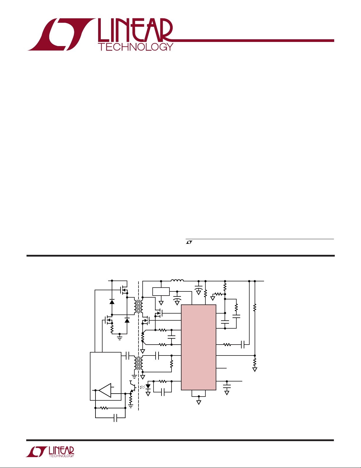
TYPICAL APPLICATIO
V
IN
36V to 72V
TG BG
LT3781
+
–
V
C
R
F
U
L1
+
C
OUT
+
110
V
PWRGD
DD
28
CG
16
FG
12
I
SNS
11
I
SNSGND
15
SYNC
5
OPTODRV
PGND GND
V
LTC1698
V
COMP
I
COMP
OVPIN
MARGIN V
V
AUX
34
Q2
R
REF
C
D1
PRISEN
SG
V
FB
F
Q1
T1
C
SG
T2
•
D2
•
R
E
ISOLATION
BOUNDARY
•
R
•
Q4
Q3
SECSEN
VDD BIAS
C
SYNC
R
SYNC
R
K
C
K
PLEASE REFER TO FIGURE 12 IN THE TYPICAL APPLICATIONS
SECTION FOR THE COMPLETE 3.3V/15A APPLICATION SCHEMATIC
Figure 1. Simplified 2-Transistor Isolated Forward Converter
R2
R1
R
FB
6
13
9
7
14
C
C
C
C
FB
C
CILM
R
CILM
MARGIN
V
AUX
3.3V
10mA
O.1µF
1681 F01
V
OUT
R5
R4
1698f
1
LTC1698
WW
W
ABSOLUTE MAXIMUM RATINGS
U
PACKAGE/ORDER INFORMATION
(Note 1)
VDD, PWRGD ....................................................... 13.2V
Input Voltage
MARGIN, VFB, OVPIN, I
SNSGND
, I
... –0.3V to 5.3V
SNS
SYNC ..................................................... –14V to 14V
Output Voltage
V
COMP
, I
(Note 2)......................... – 0.3V to 5.3V
COMP
Power Dissipation.............................................. 500mW
Operating Temperature Range
LTC1698E (Note 3)............................ –40°C to 85°C
LTC1698I........................................... – 40°C to 85°C
Storage Temperature Range ................. –65°C to 150°C
Lead Temperature (Soldering, 10 sec).................. 300°C
ELECTRICAL CHARACTERISTICS
The ● indicates specifications which apply over the full operating
V
DD
CG
PGND
GND
OPTODRV
V
COMP
MARGIN
V
FB
GN PACKAGE
16-LEAD PLASTIC SSOP
T
JMAX
T
JMAX
Consult LTC Marketing for parts specified with wider operating temperature ranges.
TOP VIEW
1
2
3
4
5
6
7
8
16-LEAD PLASTIC SO
= 125°C, θJA = 130°C/W (GN)
= 125°C, θJA = 110°C/W (SO)
FG
16
SYNC
15
V
14
I
13
I
12
I
11
PWRGD
10
OVPIN
9
S PACKAGE
AUX
COMP
SNS
SNSGND
temperature range, otherwise specifications are at TA = 25°C. VDD = 8V, unless otherwise noted. (Note 4)
U
W
ORDER PART
NUMBER
LTC1698EGN
LTC1698ES
LTC1698IGN
LTC1698IS
GN PART MARKING
1698
1698I
U
SYMBOL PARAMETER CONDITIONS MIN TYP MAX UNITS
V
DD
V
UVLO
I
VDD
MARGIN and Error Amplifier
V
FB
I
VFB
V
MARGIN
R
MARGIN
∆V
FB
G
ERR
BW
ERR
V
CLAMP
I
VCOMP
OPTODRV
G
OPTO
BW
OPTO
V
OPTOHIGH
I
OPTOSC
Supply Voltage ● 6 8 12.6 V
Undervoltage Lockout 4V
VDD Supply Current VFB, OVPIN, V
C
= CCG = 1000pF, C
FG
V
= 0V ● 1.8 4 mA
SYNC
f
= 100kHz (Note 5) 5.0 mA
SYNC
Feedback Voltage MARGIN = Open, V
Feedback Input Current VFB = 1.233V ● 0.05 1 µA
MARGIN Voltage MARGIN = Open 1.65 V
MARGIN Input Resistance 16.5 kΩ
Feedback Voltage Adjustment V
Error Amplifier Open-Loop DC Gain V
Error Amplifier Unity-Gain Bandwidth No Load (Note 6) 2 MHz
Error Amplifier Output Clamp Voltage VFB = 0V 2 V
Error Amplifier Source Current VFB = 0V ● –25 –10 mA
Error Amplifier Sink Current V
Opto Driver DC Gain OVPIN, V
Opto Driver Unity-Gain Bandwidth No Load (Note 6) 1 MHz
Opto Driver Output High Voltage VFB, OVPIN, V
Opto Driver Output Short-Circuit Current OVPIN, V
= 3.3V ● 456 %
MARGIN
V
= 0V ● –6 –5 –4 %
MARGIN
= 0.8V to 1.2V, Load = 2kΩ, 100pF ● 65 90 dB
COMP
= 5V, V
FB
I
= –10mA ● 45 V
OPTODRV
, V
ISNS
COMP
= 1.233V ● 37 mA
COMP
, V
ISNS
ISNSGND
ISNSGND
, V
ISNSGND
ISNS
= 0V,
ISNSGND
= 0.1µF,
VAUX
= 1V (Note 7) 1.223 1.233 1.243 V
● 1.215 1.233 1.251 V
= 0V ● 4.75 5 5.25 V/V
= 0V, V
= 0V, VFB = 1.233V ● –50 –25 –10 mA
= –50mV,
ISNS
2
1698f

LTC1698
ELECTRICAL CHARACTERISTICS
The ● indicates specifications which apply over the full operating
temperature range, otherwise specifications are at TA = 25°C. VDD = 8V, unless otherwise noted. (Note 4)
SYMBOL PARAMETER CONDITIONS MIN TYP MAX UNITS
V
AUX
V
AUX
Current Limit Amplifier
I
ISNSGNDISNSGND
I
ISNS
V
ILIMTH
I
ICOMPICOMP
g
mILIM
G
ICOMP
PWRGD and OVP Comparators
V
PWRGD
I
PWRGD
V
OL
V
OVPREF
I
OVPIN
t
PWRGD
t
OVP
SYNC and Drivers
V
PT
V
NT
I
SYNC
f
SYNC
t
d
t
SYNC
tr, t
t
DDIS
Note 1: Absolute Maximum Ratings are those values beyond which the life
of a device may be impaired. All voltages refer to GND.
Note 2: The LTC1698 incorporates a 5V linear regulator to power internal
circuitry. Driving these pins above 5.3V may cause excessive current flow.
Guaranteed by design and not subject to test.
Note 3: The LTC1698E is guaranteed to meet performance specifications
from 0°C to 70°C. Specifications over the –40°C to 85°C operating
temperature range are assured by design, characterization and correlation
with statistical process controls. For guaranteed performance to
specifications over the –40°C to 85°C range, the LTC1698I is available.
Note 4: All currents into device pins are positive; all currents out of the
device pins are negative. All voltages are referenced to ground unless
otherwise specified. For applications with V
Performance Characteristics.
Auxiliary Supply Voltage C
Input Current V
I
Input Current V
SNS
Current Limit Threshold V
(V
ISNS
– V
) ● –27.5 –25 –22.5 mV
ISNSGND
Source Current V
I
Sink Current V
COMP
Current Limit Amplifier V
= 0.1µF, I
VAUX
= 0V ● 0.05 1 µA
ISNSGND
= 0V ● 0.05 1 µA
ISNS
= 2.5V, V
ICOMP
= 0V, V
ISNSGND
= 0V, V
ISNSGND
= 0V, V
ISNSGND
= 0mA to 10mA, VDD = 7V to 12.6V ● 3.135 3.320 3.465 V
LOAD
= 0V –27.0 –25 –23.0 mV
ISNSGND
= –0.3V, V
ISNS
= 0.3V, V
ISNS
ICOMP
= 2.5V, I
= 2.5V (Note 8) –280 –200 – 120 µA
ICOMP
= 2.5V (Note 8) 120 200 280 µA
ICOMP
= ±10µA ● 2.2 3.5 5 millimho
ICOMP
● –370 – 200 – 80 µA
● 80 200 370 µA
Transconductance
Current Limit Amplifier V
= 2.5V, No Load ● 48 60 dB
ICOMP
Open-Loop DC Gain
Percent Below V
FB
V
↓, MARGIN = Open (Note 9) ● –9 –6 –3 %
FB
Power Good Sink Current VFB = 2V ● 10 µA
VFB = 0V ● 10 mA
Power Good Output Low Voltage I
OVPIN Threshold VFB = V
OVPIN Input Bias Current V
= 3mA, VFB = 0V ● 0.4 V
PWRGD
= V
ISNS
= 1.233V ● 0.1 1 µA
OVPIN
= 0V, OVPIN ↑ (Note 9) ● 1.18 1.233 1.28 V
ISNSGND
Power Good Response Time VFB ↑ ● 125 ms
Power Bad Response Time VFB ↓ ● 0.5 1 2.5 ms
Overvoltage Response Time V
OVPIN
↑, C
= 0.1µF ● 520 µs
OPTODRV
SYNC Input Positive Threshold ● 1 1.6 2.2 V
SYNC Input Negative Threshold ● – 2.2 –1.6 –1 V
SYNC Input Current V
SYNC Frequency Range CFG = CCG = 1000pF, V
SYNC Input to Driver Output Delay CFG = CCG = 1000pF, f
Minimum SYNC Pulse Width f
Driver Rise and Fall Time CFG = CCG = 1000pF, f
f
= ±10V ● 150 µA
SYNC
= ±5V ● 50 400 kHz
SYNC
= 100kHz, V
SYNC
= 100kHz, V
SYNC
= ±10V (Note 6) ● 75 ns
SYNC
= 100kHz, V
SYNC
= ±5V ● 40 90 ns
SYNC
= ±5V, ● 10 40 ns
SYNC
10% to 90%
Driver Disable Time-Out CFG = CCG = 1000pF, f
= 100kHz, V
SYNC
SYNC
= ±5V
Measured from CG ↑ (Note 10) ● 10 15 20 µs
Note 5: Supply current in active operation is dominated by the current
needed to charge and discharge the external FET gates. This will vary with
the LTC1698 operating frequency, supply voltage and the external FETs
used.
Note 6: This parameter is guaranteed by correlation and is not tested.
Note 7: VFB is tested in an op amp feedback loop which servos VFB to the
internal bandgap voltage.
Note 8: The current comparator output current varies linearly with
temperature.
Note 9: The PWRGD and OVP comparators incorporate 10mV of
hysteresis.
< 7V, refer to the Typical
DD
Note 10: The driver disable time-out is proportional to the SYNC period
within the frequency synchronization range.
1698f
3
LTC1698
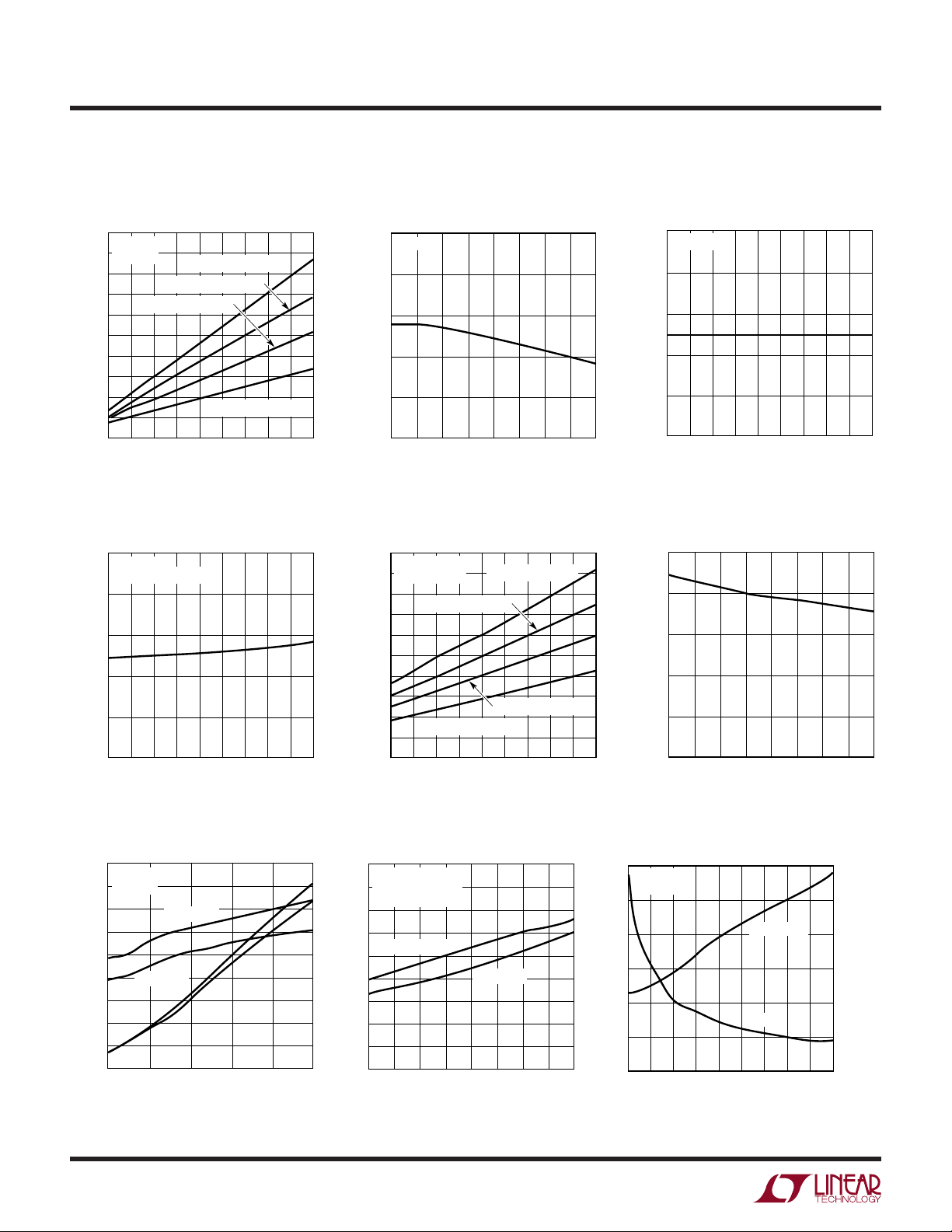
TEMPERATURE (°C)
–50
g
mILIM
(millimho)
3.8
4.2
4.6
100 125
1698 G06
3.4
3.0
–25 250 50 75 150
2.6
2.2
5.0
VDD = 8V
UW
TYPICAL PERFOR A CE CHARACTERISTICS
VFB vs Temperature
1.248
VDD = 8V
1.242
1.236
(V)
FB
V
1.230
1.224
1.218
–50
–25 0
I
Threshold vs Temperature I
SNS
–22.5
VDD = 8V
–23.0
–23.5
–24.0
–24.5
–25.0
–25.5
THRESHOLD (mV)
–26.0
SNS
I
–26.5
–27.0
–27.5
–50
–25 25
50
25 75 150
TEMPERATURE (°C)
0
50
TEMPERATURE (°C)
75
100 125
100
1698 G01
125
1698 G04
150
VFB vs V
1.248
TA = 25°C
1.242
1.236
(V)
FB
V
1.230
1.224
1.218
5
–22.5
–23.0
–23.5
–24.0
–24.5
–25.0
–25.5
THRESHOLD (mV)
–26.0
SNS
I
–26.5
–27.0
–27.5
DD
68
7
Threshold vs V
SNS
TA = 25°C
5
69
10 14
9
VDD (V)
87
VDD (V)
VFB vs V
1.295
1.282
1.270
1.258
1.245
(V)
1.233
FB
V
1.221
1.208
1.196
1.184
13
1698 G05
1.171
0
14
12
11
13
1698 G02
DD
12
10
11
MARGIN
VDD = 8V
= 25°C
T
A
0.660.33
1.320.99
V
MARGIN
1.65
1.98 2.31 2.97
(V)
Current Limit Amplifier g
vs Temperature
2.64
1698 G03
m
3.3
5
4
3
2
∆V
1
FB
(%)
0
–1
–2
–3
–4
–5
OVPIN Threshold vs Temperature OVPIN Threshold vs V
1.28
VDD = 8V
1.26
1.24
1.22
OVPIN THRESHOLD (V)
1.20
1.18
–50
–25 0
4
50
25 75 150
TEMPERATURE (°C)
100 125
1698 G07
1.28
TA = 25°C
1.26
1.24
1.22
OVPIN THRESHOLD (V)
1.20
1.18
68
7
5
DD
12
10 14
11
9
VDD (V)
13
1698 G08
Power Good Threshold
vs Temperature
1.196
VDD = 8V
1.181
1.166
1.152
1.137
POWER GOOD THRESHOLD (V)
1.122
–50
–25 0
25 75 150
TEMPERATURE (°C)
–3.0
–4.2
∆V
–5.4
FB
(%)
–6.6
–7.8
50
100 125
–9.0
1698 G09
1698f
UW
TYPICAL PERFOR A CE CHARACTERISTICS
V
vs Temperature V
AUX
3.465
VDD = 8V
= 0mA
I
LOAD
3.424
3.383
3.341
(V)
3.300
AUX
V
3.259
3.218
3.176
3.135
–25
–50
V
0
Short-Circuit Current
AUX
50
25
TEMPERATURE (°C)
vs Temperature
0
VDD = 8V
–10
–20
–30
SHORT-CIRCUIT CURRENT (mA)
–40
AUX
V
–50
–50
–25 0
50
25 75 150
TEMPERATURE (°C)
75
100
125
100 125
1698 G10
1698 G13
3.465
3.424
3.383
3.341
(V)
3.300
AUX
V
3.259
3.218
3.176
150
3.135
V
AUX
vs V
0
TA = 25°C
–10
–20
–30
SHORT-CIRCUIT CURRENT (mA)
–40
AUX
V
–50
5
vs Line Voltage V
AUX
VDD = 8V
= 0mA
I
LOAD
10
6
5
78
9
VDD (V)
11
12
Short-Circuit Current
DD
9
67
810 14
11 12 13
VDD (V)
1698 G14
AUX
3.465
VDD = 8V
= 25°C
T
A
3.424
3.383
3.341
(V)
3.300
AUX
V
3.259
3.218
3.176
13
1698 G11
14
3.135
0
Opto Driver Load Regulation
3.030
VDD = 8V
3.024
= 25°C
T
A
3.018
3.012
3.006
3.000
2.994
2.988
2.982
OPTO DRIVER OUTPUT VOLTAGE (V)
2.976
2.970
21
0
vs Load Current
1
23
4
LOAD CURRENT (mA)
67 9
43
5
LOAD CURRENT (mA)
LTC1698
5
6
7
8
1698 G12
1.0
0.8
0.6
0.4
0.2
0
–0.2
–0.4
–0.6
–0.8
1698 G15
–1.0
10
8
109
PERCENT (%)
Maximum OPTO Driver Output
Voltage vs Load Current
8
6
4
2
TA = 25°C
V
= 0V
COMP
MAXIMUM OPTO DRIVER OUTPUT VOLTAGE (V)
0
2
1
0
5
4
3
LOAD CURRENT (mA)
6
VDD = 10V
VDD = 8V
VDD = 7V
VDD = 6V
VDD = 5V
7
8
9
1698 G22
Maximum OPTO Driver Output
Voltage vs Temperature
8
6
4
2
= 0V
V
COMP
I
= –10mA
OPTODRV
MAXIMUM OPTO DRIVER OUTPUT VOLTAGE (V)
0
–50
10
–25 0 25 50
TEMPERATURE (°C)
VDD = 10V
VDD = 8V
VDD = 7V
VDD = 6V
VDD = 5V
75 100 125 150
1698 G23
Opto Driver Short-Circuit Current
vs Temperature
–10
VDD = 8V
= 1.233V
V
OPTODRV
–15
–20
–25
–30
–35
–40
–45
OPTO DRIVER SHORT-CIRCUIT CURRENT (mA)
–50
–50
–25
0
50
25
TEMPERATURE (°C)
75
100
125
1698 G16
150
1698f
5
LTC1698
VDD (V)
5
1.00
SYNC POSITIVE THRESHOLD (V)
1.24
1.72
1.96
2.20
7
9
10 14
1698 G21
1.48
68
11
12
13
TA = 25°C
UW
TYPICAL PERFOR A CE CHARACTERISTICS
I
vs SYNC Frequency
VDD
50
VDD = 8V
45
T
= 25°C
(mA)
VDD
I
A
40
35
30
25
20
15
10
5
0
50
CFG = CCG = 2200pF
150100
CFG = CCG = 4700pF
CFG = CCG = 3300pF
CFG = CCG = 1000pF
350 400
250200
300
f
(kHz)
SYNC
Opto Driver Short-Circuit Current
vs V
DD
0
TA = 25°C
= 1.233V
V
OPTODRV
–10
–20
–30
–40
OPTO DRIVER SHORT-CIRCUIT CURRENT (mA)
–50
5
67
9
810 14
11 12 13
VDD (V)
450
1698 G19
1698 G17
500
SYNC Positive Threshold
vs Temperature
2.25
VDD = 8V
2.00
1.75
1.50
1.25
SYNC POSITIVE THRESHOLD (V)
1.00
(mA)
VDD
I
20
18
16
14
12
10
8
6
4
2
0
–50
I
VDD
TA = 25°C
f
SYNC
5
–25 0
vs V
= 100kHz
CFG = CCG = 3300pF
CFG = CCG = 1000pF
76
50
25 75 150
TEMPERATURE (°C)
DD
CFG = CCG = 4700pF
98
VDD (V)
100 125
1698 G20
CFG = CCG = 2200pF
11 12
10
13
1698 G18
SYNC Positive Threshold
vs V
DD
Undervoltage Lockout Threshold
vs Temperature
5
4
3
(V)
UVLO
V
2
1
0
–50
14
–25 0
50
25 75 150
TEMPERATURE (°C)
100 125
1698 G24
Driver Rise, Fall and Propagation
Delay vs Driver Load
90
VDD = 8V
= 25°C
T
80
A
70
60
50
40
TIME (ns)
30
20
10
0
0
6
CG, FG t
2000 6000
CG, FG t
PLH
t
f
PHL
4000
DRIVER LOAD (pF)
t
SYNC Input to Driver Output Delay
vs Temperature
90
VDD = 8V
C
= CFG = 1000pF
80
CG
= 100kHz
f
SYNC
70
60
CG, FG t
r
10000
8000
1698 G25
50
(ns)
d
t
40
30
20
10
0
–50 –25 0 25 50 75 100 125 150
PLH
CG, FG t
TEMPERATURE (°C)
PHL
1698 G26
Driver Disable Time-Out vs SYNC
Frequency
30
VDD = 8V
= 25°C
T
A
25
(µs)
DISS
20
15
10
5
DRIVER DISABLE TIME-OUT t
0
100 200
150
50
t
DISS
t
DISS
300 500
350
250
f
(kHz)
SYNC
2.2
NORMALIZED DRIVER DISABLE TIME-OUT
2.0
× f
SYNC
400
450
1698 G27
1.8
1.6
1.4
1.2
1.0
t
DISS
× f
SYNC
1698f

LTC1698
U
UU
PI FU CTIO S
VDD (Pin 1): Power Supply Input. For isolated applications, a simple rectifier from the power transformer is
used to power the chip. This pin powers the opto driver,
the V
regulator powers the remaining circuitry. VDD requires an
external 4.7µF bypass capacitor.
CG (Pin 2): Catch Gate Driver. If SYNC slews positive, CG
pulls high to drive an external N-channel MOSFET. CG
draws power from the VDD pin and swings between V
and PGND.
PGND (Pin 3): Power Ground. Connect PGND to a low
impedance ground plane in close proximity to the ground
terminal of the external current sensing resistor.
GND (Pin 4): Logic and Signal Ground. GND is referenced
to the internal low power circuitry. Careful board layout
techniques must be used to prevent corruption of signal
ground reference. Connect GND and PGND together directly at the LTC1698.
OPTODRV (Pin 5): Optocoupler Driver Output. This pin
drives a ground referenced optocoupler through an external resistor. If VFB is low, OPTODRV pulls low. If VFB is
high, OPTODRV pulls high. This optocoupler driver has a
DC gain of 5. During overvoltage or overcurrent conditions, OPTODRV pulls high. The output is capable of
sourcing 10mA of current and will drive an external 0.1µF
capacitive load and is short-circuit protected.
V
COMP
is able to drive more than 2kΩ and 100pF of load. The
internal diode connected from VFB to V
OPTODRV recovery time under start-up conditions.
MARGIN (Pin 7): Current Input to Adjust the Output
Voltage Linearly. The MARGIN pin connects to an internal
16.5k resistor. The other end of this resistor is regulated
to 1.65V. Connecting MARGIN to a 3.3V logic supply
sources 100µA of current into the chip and moves the
output voltage 5% higher. Connecting MARGIN to 0V
sinks 100µA out of the pin and moves the regulated output
voltage 5% lower. The MARGIN pin voltage does not affect
the PWRGD and OVPIN trip points.
VFB (Pin 8): Feedback Voltage. VFB senses the regulated
output voltage through an external resistor divider. The
VFB pin is servoed to the reference voltage of 1.233V under
closed-loop conditions. An RC network from VFB to V
supply and the FG and CG drivers. An internal 5V
AUX
DD
(Pin 6): Error Amplifier Output. This error amplifier
reduces
COMP
COMP
compensates the feedback loop. If VFB goes low, V
pulls high and OPTODRV goes low.
OVPIN (Pin 9): Overvoltage Input. OVPIN is a high impedance input to an internal comparator. The threshold of this
comparator is set to 1.233V. If the OVPIN potential is
higher than the threshold voltage, OPTODRV pulls high
immediately. Use an external RC lowpass filter to prevent
noisy signals from triggering this comparator.
PWRGD (Pin 10): Power Good Output. This is an opendrain output. PWRGD floats if VFB is above 94% of the
nominal value for more than 2ms. PWRGD pulls low if V
is below 94% of the nominal value for more than 1ms. The
PWRGD threshold is independent of the MARGIN pin
potential.
I
SNSGND
positive side of the sense resistor, normally grounded.
I
SNS
tive side of the sense resistor through an external RC
lowpass filter. This pin normally sees a negative voltage,
which is proportional to the average load current. If
current limit is exceeded, OPTODRV pulls high.
I
COMP
at this pin compensates the current limit feedback loop.
Referencing the RC to V
shoot on start-up. This pin can float if current limit loop
compensation is not required.
V
AUX
requires a 0.1µF or greater bypass capacitor. This auxiliary
power supply can power external devices and sources
10mA of current. Internal current limiting is provided.
SYNC (Pin 15): Drivers Synchronization Input. A negative
voltage slew at SYNC forces FG to pull high and CG to pull
low. A positive voltage slew at SYNC resets the FG pin and
CG pulls high. If SYNC loses its synchronization signal for
more than the driver disable time-out interval, both the
forward and catch drivers output are forced low. The SYNC
circuit accepts pulse and square wave signals. The minimum pulse width is 75ns. The synchronization frequency
range is between 50kHz to 400kHz.
FG (Pin 16): Forward Gate Driver. If SYNC slews negative,
FG goes high. FG draws power from VDD and swings
between VDD and PGND.
(Pin 11): Current Sense Ground. Connect to the
(Pin 12): Current Sense Input. Connect to the nega-
(Pin 13): Current Amplifier Output. An RC network
controls output voltage over-
OUT
(Pin 14): Auxiliary 3.3V Logic Supply. This pin
COMP
FB
1698f
7
LTC1698
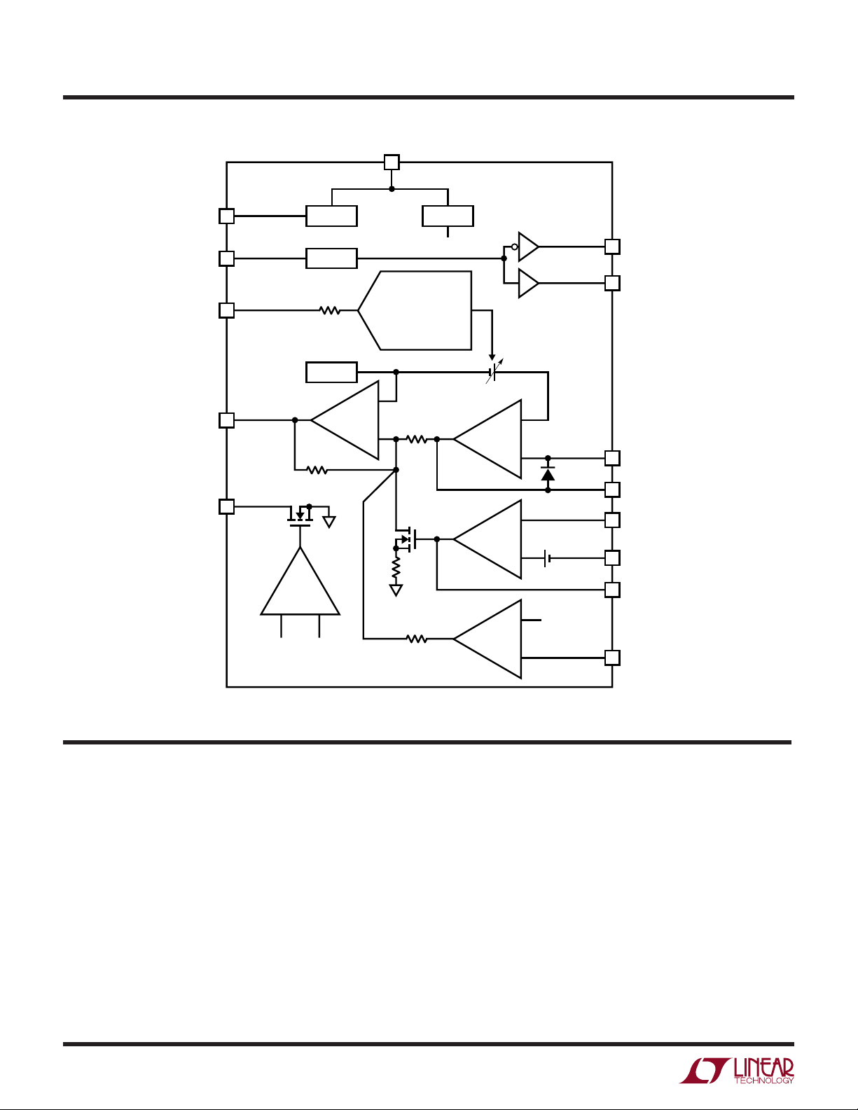
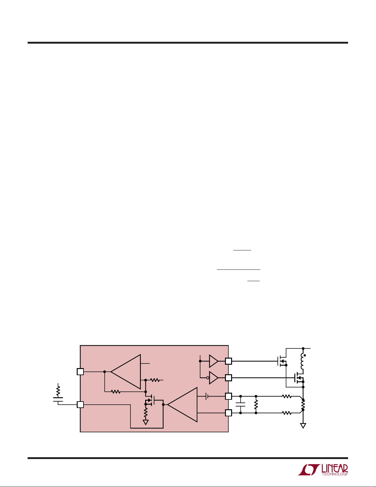
BLOCK DIAGRA
V
14
SYNC
15
MARGIN
7
W
AUX
1
V
DD
AUX GEN VCC GEN
V
SYNC IN
R
MARGIN
I-TO-V CONVERTER
CC
CG
FG
16
2
OPERATIO
OPTODRV
5
PWRGD
10
–
V
U
(Refer to Block Diagram)
M
PWRGD
PWRGD
FB
BANDGAP
100k
+
0.94V
REF
OPTO
V
REF
±5% V
REF
+
20k
–
M
ILIM
R
ILIM
3k
R
OVP
3k
+
ERR
–
+
I
LIM 25mV
+
–
+
OVP
–
V
FB
8
V
COMP
6
I
SNSGND
11
I
SNS
12
I
COMP
13
V
REF
OVPIN
9
1698 BD
The LTC1698 is a secondary-side synchronous rectifier
controller designed to work with the LT3781 primary-side
synchronous controller chip to form an isolated synchronous forward converter. This chip set uses a dual transistor forward topology that is predominantly used in distributed power supply systems where isolated low voltages
are needed to power complex electronic equipment. The
primary stage is a current mode, fixed frequency forward
converter and provides the typical PWM operation. A
power transformer is used to provide the functions of
input/output isolation and voltage step-down to achieve
the required low output voltage. Instead of using typical
8
Schottky diodes, synchronous rectification on the secondary offers isolation with high efficiency. It supplies
high power without the need of bulky heat sinks, which is
often a problem in any space constrained application.
The LTC1698 not only provides synchronous drivers for
the external MOSFETs, it comes with other housekeeping
functions performed on the secondary side of the power
supply, all within a single integrated controller. Figure 1
shows the typical chip-set application. Upon power up, the
LTC1698’s VDD input is low, the gate drivers TG and BG are
both at the ground potential. The secondary forward and
1698f

OPERATIO
LTC1698
U
(Refer to Block Diagram)
catch MOSFETs Q3 and Q4 are off. As soon as transistors
Q1 and Q2 turn on, the flux in the power transformer T1
forces the body diodes of Q3 and Q4 to conduct, and the
whole circuit starts like a conventional forward converter.
At the same time, the LTC1698 VDD potential ramps up
quickly through the VDD bias circuitry. Once the V
DD
voltage exceeds 4.0V, the LTC1698 enables its drivers and
enters synchronous operation.
The pulse transformer T2 synchronizes the primary and
secondary MOSFET drivers. In a typical conversion cycle,
the primary MOSFETs Q1 and Q2 turn on simultaneously.
SG goes low and generates a negative spike at the LTC1698
SYNC input through the pulse transformer. The LTC1698
forces FG to turn on and CG to turn off. Power is delivered
to the load through the transformer T1 and the inductor L1.
At the beginning of the next phase in which Q1 and Q2 turn
off, SG goes high, SYNC sees a positive spike, the MOSFET
Q3 shuts off, Q4 conducts and allows continuous current
to flow through the inductor L1. The capacitor C
OUT
filters
the switching waveform to provide a steady DC output
voltage for the load.
The LTC1698 error amplifier ERR senses the output voltage through an external resistor divider and regulates the
VFB pin potential to the 1.233V internal bandgap voltage.
An external RC network across the VFB and V
COMP
pins
frequency compensates the error amplifier feedback. The
opto driver amplifies the voltage difference between the
V
pin and the bandgap potential, driving the external
COMP
optocoupler diode with an inverting gain of 5. The
optocoupler feeds the amplified output error signal to the
primary controller and closes the forward converter voltage feedback loop. Under start-up conditions, the internal
diode across the LTC1698 error amplifier clamps the
V
pin. This speeds up the opto driver recovery time by
COMP
reducing the negative slew rate excursion at the COMP pin.
The forward converter output voltage can be easily ad-
justed. The potential at the MARGIN pin is capable of
forcing the error amplifier reference voltage to move
linearly by ±5%. The internal R
MARGIN
resistor converts
the MARGIN voltage to a current and linearly controls the
offset of the error amplifier. Connecting the MARGIN pin
to 3.3V increases the VFB voltage by 5%, and connecting
the MARGIN pin to 0V reduces VFB by 5%. With the
MARGIN pin floating, the VFB voltage is regulated to the
internal bandgap voltage.
The current limit transconductance amplifier I
provides
LIM
the secondary side average current limit function. The
average voltage drops across the R
SECSEN
resistor is
sensed and compared to the –25mV threshold set by the
internal I
amplifier. Once I
LIM
detects high output
LIM
current, the current amplifier output pulls high, overrides
the error amplifier, injects more current into the photo
diode and forces a lower duty cycle. An RC network
connected to the I
pin is used to stabilize the second-
COMP
ary current limit loop. Alternatively, if only overcurrent
fault protection is required, I
COMP
can float.
If under abnormal conditions the feedback path is broken,
OVPIN provides another route for overvoltage fault protection. If the voltage at OVPIN is higher than the bandgap
voltage, the OVP comparator forces OPTODRV high immediately. A simple external RC filter prevents a momentary overshoot at OVPIN from triggering the OVP
comparator. Short OVPIN to ground if this pin is not used.
The LTC1698 provides an open-drain PWRGD output. If
VFB is less than 94% of its nominal value for more than
1ms, the PWRGD comparator pulls the PWRGD pin low.
If VFB is higher than 94% of its nominal value for more than
2ms, the transistor M
shuts off, and an external
PWRGD
resistor pulls the PWRGD pin high.
The LTC1698 provides an auxiliary 3.3V logic power
supply. This auxiliary power supply is externally compensated with a minimum 0.1µF bypass capacitor. It supplies
up to 10mA of current to any external devices.
1698f
9

LTC1698
WUUU
APPLICATIO S I FOR ATIO
Undervoltage Lockout
In UVLO (low VDD voltage) the drivers FG and CG are shut
off and the pins OPTODRV, V
, PWRGD and I
AUX
COMP
are
forced low. The LTC1698 allows the bandgap and the
internal bias currents to reach their steady-state values
before releasing UVLO. Typically, this happens when V
DD
reaches approximately 4.0V. Beyond this threshold, the
drivers start switching. The OPTODRV, V
I
pins return to their normal values and the chip is
COMP
, PWRGD and
AUX
fully functional. However, if the VDD voltage is less than 7V,
the OPTODRV and V
current sourcing capabilities are
AUX
limited. See the OPTO driver graphs in the Typical Performance Characteristics section.
VDD Regulator
The bias supply for the LTC1698 is generated by peak
rectifying the isolated transformer secondary winding. As
shown in Figure 2, the zener diode Z1 is connected from
base of Q5 to ground such that the emitter of Q5 is
regulated to one diode drop below the zener voltage. RZ is
selected to bring Z1 into conduction and also provide base
current to Q5. A resistor (on the order of a few hundred
ohms), in series with the base of Q5, may be required to
surpress high frequency oscillations depending on Q5’s
selection. A power MOSFET can also be used by increasing
the zener diode value to offset the drop of the gate-tosource voltage. VDD supply current varies linearly with the
supply voltage, driver load and clock frequency. A 4.7µF
bypass capacitor for the VDD supply is sufficient for most
applications. This capacitor must be large enough to
provide a stable DC voltage to meet the LTC1698 V
DD
supply requirement. Under start-up conditions, it must be
small enough to power up instantaneously, enabling the
LTC1698 to regulate the feedback loop. Using a larger
capacitor requires evaluation of the start-up performance.
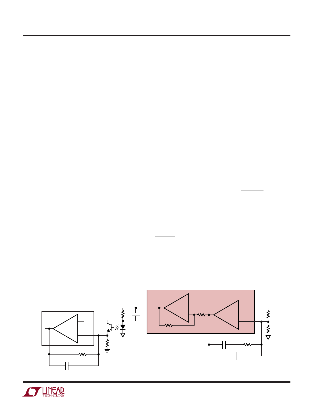
SYNC Input
Figure 3 shows the synchronous forward converter application. The primary controller LT3781 runs at a fixed
frequency and controls MOSFETs Q1 and Q2. The secondary controller LTC1698 controls MOSFETs Q3 and Q4. An
inexpensive, small-size pulse transformer T2 synchronizes the primary and the secondary controllers. Figure 4
shows the pulse transformer timing waveforms. When the
LT3781 synchronization output SG goes low, MOSFET
V
IN
PRIMARY
CONTROLLER
LT3781
SG
TG
BG
Q1
D1
Q2 Q3
C
SG
ISOLATION BARRIER
••
D2
••
T2
Q4
T1
C
SYNC
R
CG
FG
SYNC
Figure 3. Synchronization Using Pulse Transformer
L1
SECONDARY
CONTROLLER
LTC1698
SYNC
1698 F03
SECONDARYPRIMARY
V
OUT
C
OUT
10
V
SECONDARY
1Ω
D3
0.47µF
*RB IS OPTIONAL, SEE TEXT
Figure 2. VDD Regulator
TG
BG
SG
R
Z
2k
*
R
B
Q5
FZT690
Z1
10V
4.7µF
1698 F02
V
DD
SYNC
FG
CG
1698 F04
Figure 4. Primary Side and Secondary Side
Synchronization Waveforms
1698f

WUUU
APPLICATIO S I FOR ATIO
LTC1698
drivers TG and BG go high. The pulse transformer T2
generates a negative slew at the SYNC pin and forces the
secondary MOSFET driver FG to go high and CG to go low.
When TG and BG go low, SG goes high and the secondary
controller forces CG high and FG low.
For a given pulse transformer, a bigger capacitor C
SG
generates a higher and wider SYNC pulse. The peak of this
pulse should be much higher than the SYNC threshold.
Amplitudes greater than ±5V help to speed up the SYNC
comparator and reduce the SYNC to FG and CG drivers
propagation delay. The minimum pulse width is 75ns.
Overshoot during the pulse transformer reset interval
must be minimized and kept below the minimum comparator thresholds of ±1V. The amount of overshoot can
be reduced by having a smaller reset resistor R
SYNC
. For
nonisolated applications, the SYNC input can be driven
directly by a square pulse. To reduce the propagation
delay, make the positive and negative magnitude of the
square wave much greater than the ±2.2V maximum
threshold.
In addition to the simple driver synchronization, the secondary controller requires a driver disable signal. Loss of
synchronization while CG is high will cause Q4 to discharge the output capacitor. This produces a negative
output voltage transient and possible damage to the load
circuitry connected to V
. To overcome this problem,
OUT
the LTC1698 comes with a unique adaptive time-out
circuit. It works well within the 50kHz to 400kHz frequency
range. At every positive SYNC pulse, the internal timer
resets. If the SYNC signal is missing, the internal timer
loses its reset command, and eventually exceeds the
internal time-out limit. This forces both the FG and CG
drivers to go low immediately.
The time-out duration varies linearly with the LT3781
primary controller clocking frequency. Upon power up,
the time-out circuitry takes a few clock cycles to adapt to
the input clock frequency. During this time interval, the
drivers pulse width might be prematurely terminated, and
the inductor current flows through the MOSFETs body
diode. Once the LTC1698 timer locks to the clocking
frequency, the LTC1698 drivers follow the SYNC signal
without fail. Figure 5 shows the SYNC time-out wave-
SG
SYNC
FG
CG
RESET
(INTERNAL)
DISDRI
(INTERNAL)
Figure 5. SYNC Time-Out Waveforms
1698 F05
forms. The time-out circuit guarantees that if the SYNC
pulse is missing for more than one period, both the
drivers will be shut down preventing the output voltage
from going below ground. The wide synchronization
frequency range adds flexibility to the forward converter
and allows this converter chip set to meet different
application requirements.
Under normal operating conditions, the time-out circuitry
adapts to the switching frequency within a few cycles.
Once synchronized, internal circuitry ensures the maximum time that the Catch FET (Q4) could be left turned on
is typically just over one switching period. This is particularly important with high output voltages that can generate
significant negative output inductor currents if the Catch
FET Q4 is left on. Poor feedback loop performance including output voltage overshoot can cause the primary controller to interrupt the synchronization pulse train. While
this generally is not a problem, it is possible that low
frequency interruptions could lead to a time-out period
longer than a switching period, limited only by the internal
timer clamp (50µs typical).
Output Voltage Programming
The switching regulator output voltage is programmed
through a resistor feedback network (R1 and R2 in
Figure 1) connected to VFB. If the output is at its nominal
value, the divider output is regulated to the error amplifier
threshold of 1.233V.
The output voltage is thus set according to the relation:
V
= 1.233 • (1 + R2/R1)
OUT
1698f
11

LTC1698
WUUU
APPLICATIO S I FOR ATIO
MARGIN Adjustment
The MARGIN input is used for adjusting the programmed
output voltage linearly by varying the current flowing into
and out of the pin. Forcing 100µA into the pin moves the
output voltage 5% higher. Forcing 100µA out of the pin
moves the output voltage 5% lower. With the MARGIN pin
floating, the VFB pin is regulated to the bandgap voltage of
1.233V. The MARGIN pin is a high impedance input. It is
important to keep this pin away from any noise source like
the inductor switching node. Any stray signal coupled to
the MARGIN pin can affect the switching regulator output
voltage.
This pin is internally connected to a 16.5k resistor that
feeds the I-V converter. The I-V converter output linearly
controls the error amplifier offset voltage. The input of the
I-V converter is biased at 1.65V. This allows the ±100µA
current to be obtained by connecting the MARGIN pin to
the V
3.3V supply (+5%) or GND (– 5%). For output
AUX
voltage adjustment smaller than ±5%, an external resistor
R
as shown in Figure 6 is added in series with the
EXT
internal resistor to lower the current flowing into or out of
the MARGIN pin. The value of R
R
=
EXT
5
%
REQUIRED
%
is calculated as follow:
EXT
1165
–•.
k
VFB loop causes the error amplifier to drive the OPTODRV
pin low, forcing the primary controller to increase the duty
cycle. This causes the output voltage to increase to a
dangerously high level. To eliminate this fault condition,
the OVP comparator monitors the output voltage with a
resistive divider at OVPIN. A voltage at OVPIN higher than
the V
potential forces the OPTODRV pin high and
REF
reduces the duty cycle, thus preventing the output voltage
from increasing further.
The OVPIN senses the output voltage through a resistor
divider network (R4 and R5 in Figure 1). The divider is
ratioed such that the voltage at OVPIN equals 1.233V when
the output voltage rises to the overvoltage level. The
overvoltage level is set following the relation:
V
OVERVOLTAGE
= 1.233 • (1 + R5/R4)
The OVP comparator is designed to respond quickly to an
overvoltage condition. A small capacitor from OVPIN to
ground keeps any noise spikes from coupling to the OVP
pin. This simple RC filter prevents a momentary overshoot
from triggering the OVP comparator.
The OVP comparator threshold is independent of the
potential at the MARGIN pin. If the OVP function is not
used, connect OVPIN to ground.
Power Good
R
REDUCE
V
FB
V
AUX
3.3V
EXT
(OPTIONAL)
INCREASE
V
FB
0.1µF
Figure 6. Output Voltage Adjustment
7
14
MARGIN
V
AUX
R
MARGIN
V
AUX GEN
DD
I-V CONVERTER
BANDGAP
ERR
V
REF
±5% V
REF
+
V
FB
V
COMP
8
6
1698 F06
–
Overvoltage Function
The OVPIN is used for overvoltage protection and is
designed to protect against an open VFB loop. Opening the
12
The PWRGD pin is an open-drain output for power good
indication. PWRGD floats if VFB is above 94% of the
nominal value for more than 2ms. An external pull-up
resistor is required for PWRGD to swing high. PWRGD
pulls low if VFB drops below 94% of the nominal value for
more than 1ms. The PWRGD threshold is referenced to the
1.233V bandgap voltage, which remains unchanged if the
MARGIN pin is exercised.
Opto Feedback and Frequency Compensation
For a forward converter to obtain good load and line
regulation, the output voltage must be sensed and compared to an accurate reference potential. Any error voltage
must be amplified and fed back to the supply’s control
circuitry where the sensed error can be corrected. In an
isolated supply, the control circuitry is frequently located
on the primary. The output error signal in this type of
1698f
WUUU
APPLICATIO S I FOR ATIO
LTC1698
supply must cross the isolation boundary. Coupling this
signal requires an element that will withstand the isolation
potentials and still transfer the loop error signal.
Optocouplers are widely used for this function due to their
ability to couple DC signals. To properly apply them, a
number of factors must be considered. The gain, or
current transfer ratio (CTR) through an optocoupler is
loosely specified and is a strong function of the input
current through the diode. It changes considerably as a
function of time (aging) and temperature. The amount of
aging accelerates with higher operating current. This
variation directly affects the overall loop gain of the system. To be an effective optical detector, the output transistor of the optocoupler must have a large base area to
collect the light energy. This gives it a large collector to
base capacitance which can introduce a pole into the
feedback loop. This pole varies considerably with the
current and interacts with the overall loop frequency
compensation network.
The common collector optocoupler configuration removes
the miller effect due to the parasitic capacitance and
increases the frequency response. Figure 7 shows the
optocoupler feedback circuitry using the common collector approach. Note that the terms RD, CTR, CDE and rπ vary
from part to part. They also change with bias current. The
dominant pole of the opto feedback is due to RF and CF. The
feedforward capacitor CK at the optocoupler creates a low
frequency zero. This zero should be chosen to provide a
phase boost at the loop crossover frequency. The parallel
combination of RK and RD form a high frequency pole with
CK. For most optocouplers, RD is 50Ω at a DC bias of 1mA,
and 25Ω at a DC bias of 2mA. The CTR term is the small
signal AC current transfer ratio. For the QT Optoelectronics MOC207 optocoupler used here, the AC CTR is around
1, even though the DC CTR is much lower when biased at
1mA or 2mA. The first denominator term in the VC/V
OUT
equation has been simplified and assumes that CFB<<CC.
The actual term is:
sR C C sR
••( )• ••
21++
CFB C
CC
CFB
CC
CFB
•
+
+
(••)
V
C
=
–
V
OUT
wherewhere
R Optocoupler diode equivalentsmall signalresis ce
D
CTR Optocoupler current transferratio
C Optocoupler nonlinearcapacitor acrossbase to emitter
DE
r Optocoupler small signalresis ce across the base emitter
π
(••)•( •• )
sR C sR C
:
=−
=
=
=−
LT3781
1
sC R
21
CCFB
+
–
V
C
C
F
CC
+
V
REF
V
FB
R
F
••
5
tan
V
CC
R
E
+
(••)
1
sR C
KK
+
••
1
sC
C
K
K
RR
OPTODRV
R
K
MOC207
•
RR
KD
+
KD
tan
100k
R CTR
•
RR srC sRC
+
–
•
F
+
DK DE FF
•
(••)•(••)
V
REF
20k
V
COMP
1
++
1
π
LTC1698
V
+
REF
V
FB
–
C
C
R
C
C
FB
1698 F07
1
1
V
OUT
R2
R1
Figure 7. Error Signal Feedback
1698f
13
LTC1698
WUUU
APPLICATIO S I FOR ATIO
A series RC network can be added in parallel with R2
(Figure 7) to provide a zero for the feedback loop frequency compensation.
The opto driver will drive a capacitive load up to 0.1µF. For
optocouplers with a base pin, switching signal noise can
get into this high impedance node. Connect a large resistor, 1M or 2M between the base and the emitter. This
increases the diode current and the overall feedback
bandwidth slightly, and decreases the optocoupler gain.
When designing the resistor in series with the optocoupler
diode, it is important to consider the part to part variations
in the current transfer ratio and its reduction over temperature and aging. The bigger the biasing current, the
faster the aging. The LTC1698 opto driver is designed to
source up to 10mA of current and swing between 0.4V to
(V
– 2.5V). This should meet the design consideration
DD
of most optocouplers.
Besides the voltage feedback function, the LTC1698 opto
driver couples fault signals to the primary controller and
prevents catastrophic damage to the circuit. Upon current
limit or an overvoltage fault, the I
or OVP comparator
LIM
overrides the error amplifier output and forces the
OPTODRV pin high. This sources maximum current into
the external optodiode and reduces the forward converter
duty cycle.
Average Current Limit
The secondary current limit function is implemented by
measuring the negative voltage across the current sense
resistor R
SECSEN
. The current limit transconductance
amplifier I
Figure 8, if the secondary current is small, the I
goes low and the transistor M
at V
COMP
ary current is large, I
sistor M
has a –25mV threshold. As shown in
LIM
pin
COMP
shuts off. The potential
ILIM
determines the OPTODRV output. If the second-
pulls high and forces the tran-
COMP
to turn on hard. Thus the current limit circuit
ILIM
overrides the voltage feedback and forces OPTODRV high
and injects maximum current into the external optocoupler.
The R
resistor provides a linear relationship between
ILIM
the current sensed and the OPTODRV output.
The I
SNS
and I
SNSGND
pins allow a true Kelvin current
sense measurement and offer true differential measurement across the sense resistor. A differential lowpass
filter formed by R6 and C2 removes the pulse-to-pulse
inductor current ripple and generates the average secondary current which is equal to the load current. The
lowpass corner frequency is typically set to 1 to 2 orders
of magnitude below the switching frequency and follows
the relationship:
mV
R
SECSEN
6
R
=
25
=
I
LMAX
1
f
π
22
•• •
SW
C
10
where:
R
I
LMAX
f
SW
= Secondary current sense resistor
SECSEN
= Maximum allowed secondary current
= Forward converter switching frequency
14
DRIVE
V
+
OPTODRV
5
V
OUT
R
CILM
C
CILM
I
COMP
13
LTC1698
OPTO
100k
M
REF
20k
–
ILIM
Figure 8. Secondary Average Current Limit
V
COMP
–
I
LIM
R
ILIM
3k
+
25mV
+
I
I
SNSGND
CG
SNS
2
FG
16
12
11
C2
R
DIV
(OPTIONAL)
R6
R6
T1
Q4
Q3
R
SECSEN
1698 F08
1698f

WUUU
APPLICATIO S I FOR ATIO
LTC1698
If the application generates a bigger current sense voltage,
a potential divider can be easily obtained by adding a
resistor across C2. With this additional resistor, the voltage sensed by the current comparator becomes:
R
DIV
+(• )
RR
DIV
26
An RC network formed by R
and V
can be used to stabilize the current limit loop.
OUT
Connecting the compensation network to V
•
V
RSENSE
CILM
and C
between I
CILM
minimizes
OUT
COMP
output overshoot during start-up or short-circuit recovery. The R
CILM
and C
zero should be chosen to be well
CILM
within the closed-loop crossover frequency. This pin can
be left floating if current loop compensation is not required. The forward converter secondary current limit function can be disabled by shorting I
SNS
and I
SNSGND
to ground.
Auxiliary 3.3V Logic Power Supply
An internal P-channel LDO (low dropout regulator) produces the 3.3V auxiliary supply that can power external
devices or drive the MARGIN pin. This supply can source
up to 10mA of current and the current limit is provided
internally. The pin requires at least a 0.1µF bypass
capacitor.
MOSFET Selection
Two logic-level N-channel power MOSFETs (Q3 and Q4 in
Figure 1) are required for most LTC1698 circuits. They are
selected based primarily on the on-resistance and body
diode considerations. The required MOSFET R
DS(ON)
should
be determined based on input and output voltage, allowable power dissipation and maximum required output
current.
The average inductor (L1) current is equal to the output
load current. This current is always flowing through either
Q3 or Q4 with the power dissipation split up according to
the duty cycle:
DC Q
() •
() – •
DC Q
V
3
=
41
=
N
OUTINP
V
N
V
OUTINP
V
S
N
N
S
The R
required for a given conduction loss can now
DS(ON)
be calculated by rearranging the relation P = I2R.
PIRDCQ
MAX Q MAX DS ON Q
⇒=
PIRDCQ
MAX Q MAX DS ON Q
⇒=
where I
=
() ()
3
R
()
DS ON Q
=
() ()
4
R
()
DS ON Q
is the maximum load current and P
MAX
2
••()
P
3
4
MAX Q
2
IDCQ
MAX
2
••()
P
MAX Q
2
IDCQ
MAX
3
()
3
•()
•()
4
()
4
3
4
3
4
is the
MAX
allowable conduction loss.
In a typical 2-transistor forward converter circuit, the duty
cycle is less than 50% to prevent the transformer core
from saturating. This results in the duty cycle of Q4 being
greater than that of Q3. Q4 will dissipate more power due
to the higher duty cycle. A lower R
MOSFET can be
DS(ON)
used for Q4. This will slow down the turn-on time of Q4
since a lower R
MOSFET will have a larger gate
DS(ON)
capacitance.
The next consideration for the MOSFET is the characteris-
tic of the body diode. The body diodes conduct during the
power-up phase, when the LTC1698 VDD supply is ramping up and the time-out circuit is adapting to the SYNC
input frequency. The CG and FG signals terminate prematurely and the inductor current flows through the body
diodes. The body diodes must be able to take the comparable amount of current as the MOSFETs. Most power
MOSFETs have the same current rating for the body diode
and the MOSFET itself.
The LTC1698 CG and FG MOSFET drivers will dissipate
power. This will increase with higher switching frequency,
higher VDD or larger MOSFETs. To calculate the driver
dissipation, the total gate charge Qg is used. This parameter is found on the MOSFET manufacturers data sheet.
The power dissipated in each LTC1698 MOSFET driver is:
P
DRIVER
= Qg • VDD • f
SW
where fSW is the switching frequency of the converter.
where NP/NS is the turns ratio of the transformer T1.
1698f
15

LTC1698
t
DC MIN
f
OFF MAXSW()
–()
=
()
1
DC MIN
N
NVV
P
S
OUT
IN MAX
() •
()
=
WUUU
APPLICATIO S I FOR ATIO
Power Transformer Selection
The forward transformer provides DC isolation and delivers energy from the primary to the secondary. Unlike the
flyback topology, the transformer in the forward converter
is not an energy storage device. As such, ungapped ferrite
material is typically used. Select a power material rated
with low loss at the switching frequency. Many core
manufacturers have selection guides and application notes
for transformer design. A brief overview of the more
important design considerations is presented here.
For operating frequencies greater than 100kHz, the flux
in the core is usually limited by core loss, not saturation.
It is important to review both criteria when selecting the
trans
former. The AC operating flux density for core loss is
given by:
VDC
••
B
AC
IN
=
NAf
•••
2
PeSW
10
8
where:
BAC is the AC operating flux density (gauss)
The core must be sized to provide sufficient window area
for the amount of wire and insulation needed. The best
performance is achieved by making each winding a single
layer evenly distributed across the width of the bobbin.
Multiple layers may be used to increase the copper area.
Interleaving the primary and secondary windings will
decrease the leakage inductance.
In a single-ended forward converter, much of the energy
stored in the leakage inductance is dissipated in the
primary-side MOSFET during turn-off. It is good design
practice to sandwich the secondary winding between two
primary windings.
For the 2-transistor forward converter shown in Figure 1,
energy stored in the leakage inductance is returned to the
input by diodes D1 and D2. With this topology, additional
insulation for higher isolation can be used without significant penalty.
For a more detailed discussion on transformer core and
winding losses, see Application Note AN19.
Inductor Selection
DC is the operating duty cycle
Ae is the effective cross sectional core area (cm2)
fSW is the switching frequency
To prevent core saturation during a transient condition,
the peak flux density is:
V DC MAX
=
IN MAX
B
PK
•( )•
()
NAf
••
PeSW
10
8
The minimum secondary turns count is:
VV
+
NN
S MIN P
()
•
=
OUT D
V DC MAX
IN MIN
()
•( )
where:
V
is the secondary output voltage
OUT
VD is the voltage drop across the rectifier in the secondary
V
is the minimum input voltage
IN(MIN)
DC(MAX) is the maximum duty cycle
The output inductor in a typical LTC1698 circuit is chosen
for inductance value and saturation current rating. The
output inductor in a forward converter operates the same
as in a buck regulator. The inductance sets the ripple
current, which is commonly chosen to be 40% of the full
load current. Ripple current is set by:
Vt
•
I
RIPPLE
OUT OFF MAX
=
()
L
where:
and DC(MIN) is calculated based on the maximum input
voltage.
16
1698f

WUUU
APPLICATIO S I FOR ATIO
LTC1698
Once the value of the inductor has been determined, an
inductor with sufficient DC current rating is selected. Core
saturation must be avoided under all operating conditions.
Under start-up conditions, the converter sees a short
circuit while charging the output capacitor. If the inductor
saturates, the peak current will dramatically increase. The
current will be limited only by the primary controller
minimum on time and the circuit impedances.
High efficiency converters generally cannot afford the core
loss found in low cost iron powder cores, forcing the use
of more expensive ferrite, molypermalloy, or Kool Mµ
®
cores. As inductance increases, core loss goes down.
Increased inductance requires more turns of wire so
copper losses will increase. The optimum inductor will
have equal core and copper loss.
Ferrite designs have very low core losses and are preferred
at higher switching frequencies. Therefore, design goals
concentrate on minimizing copper loss and preventing
saturation. Kool Mµ is a very good, low-loss powder
material with a “soft” saturation characteristic.
Molypermalloy is more efficient at higher switching frequencies, but is also more expensive. Surface mount
designs are available from many manufacturers using all
of these materials.
Output Capacitor Selection
The output capacitor selection is primarily determined by
the effective series resistance (ESR) to minimize voltage
ripple. In a forward converter application, the inductor
current is constantly flowing to the output capacitor,
therefore, the ripple current at the output capacitor is
small. The output ripple voltage is approximately given by:
V I ESR
RIPPLE RIPPLE
≈+
•
fC
••
8
SW OUT
1
The output ripple is highest at maximum input voltage
since I
the ESR requirement for C
increases with input voltage. Typically, once
RIPPLE
has been satisfied the
OUT
capacitance is adequate for filtering and has the required
RMS current rating.
Fast load current transitions at the output will appear as a
voltage across the ESR of the output capacitor until the
feedback loop can change the inductor current to match
the new load current value. As an example: at 3.3V out, a
10A load step with a 0.01Ω ESR output capacitor would
experience a 100mV step at the output, a 3% output
change. In surface mount applications, multiple capacitors may have to be placed in parallel to meet the ESR
requirement.
PC Board Layout Checklist
When laying out the printed circuit board, the following
checklist should be used to ensure proper operation of the
LTC1698. These items are also illustrated graphically in
Figure 9. Check the following for your layout:
1. Keep the power circuit and the signal circuit segregated. Place the power circuit, shown in bold, so that
the two MOSFET drain connections are made directly at
the transformer. The two MOSFET sources should be as
close together as possible.
2. Connect PGND directly to the sense resistor with as
short a path as possible. The MOSFET gate drive return
currents flow through this connection.
3. Connect the 4.7µF ceramic capacitor directly between
VDD and PGND. This supplies the FG and CG drivers and
must supply the gate drive current.
4. Bypass the V
supply with a 0.1µF ceramic capacitor
AUX
returned to GND.
5. Place all signal components in close proximity to their
associated LTC1698 pins. Return all signal component
grounds directly to the GND pin. One common connection can be made to V
+
from R2, R5 and C
OUT
CILM
.
6. Make the connection between GND and PGND right at
the LTC1698 pins.
7. Use a Kelvin-sense connection from the I
SNS
and I
SNSGND
pins to the secondary-side current-limit resistor
R
Kool Mµ is a registered trademark of Magnetics, Inc.
SECSEN
.
1698f
17

LTC1698
WUUU
APPLICATIO S I FOR ATIO
T1
•
•
Q3
MOC207
Q4
C4
T2
•
•
BOLD LINES INDICATE HIGH CURRENT PATHS
1Ω
R
D3
R2R7
R
K
R1
C
K
R
Figure 9. LTC1698 Layout Diagram
L1
SECSEN
C
4.7µF
C
+
V
OUT
+
C
OUT
–
V
OUT
SYNC
V
I
COMP
I
SENSGND
PWRGD
OVPIN
16
FG
15
14
AUX
13
12
I
SNS
11
10
9
0.1µF
R
C
CILM
CILM
0.1µF
0.1µF
R5
1k
1k
R4
1698 F09
1
V
DD
LTC1698
2
CG
3
PGND
GND
4
5
OPTODRV
6
V
COMP
C
7
C
MARGIN
FB
8
V
FB
36V
TO 72V
+
220Ω
V
OUT1
3.3V
AT 10A
V
OUT2
1.8V
AT 10A
C
OUT2
1698 F10
L1
V
IN
••
BG
TG
V
C
LT3781
SG
V
REF
+
V
FB
–
ISOLATION
BOUNDARY
••
V
BIAS
CC
V
DD
V
CG
FG
I
SNS
LTC1698
SYNC
OPTODRV
GND
COMP
10k
V
BOOST
GBIAS
SW
VA
OUT
V
CMDSH-3
4.7µF
L2
TG
0.1µF
BG
3.3k
33nF
FB
+
Q1
1.8µH
Q2 B340A
0.006Ω
4700pF
3.01k
2.32k
CC
10pF
V
FB
180pF
680pF
10k
C
OUT2
L2: SUMIDA CEP125-IR8MC-H
Q1, Q2: SILICONIX Si7440DP
SYNC
CSET
C
S
ILCOMP
SS
0.01µF
BGS
PGND
CL–CL
: POSCAP, 680µF/4V
LT3710
Figure 10. Simplified Single Secondary Winding 3.3V and 1.8V Output Isolated DC/DC Converter
18
1698f

TYPICAL APPLICATIO S
V
CC
13
2
1
5
1µF
0.01µF
82pF
OVLO
SHDN
1.24k
1%
10k
4.7µF
16V
1000pF
5V
REF
6
F
SET
0.1µF
8
SS
10
12
T2
PULSE ENG
P2033
BAS21
BAS21
BAT54
BAT54S
ZVN3310F
9
V
C
PGND
14
V
FB
37
4
THERM
LT3781
SYNC SGND
52.3k
1%
10Ω
1k
3k
1k
3.3k
FZT690B
0.22µF
50V
1
10k
220pF
MOC207
143
1
4
8
7
5
14
15
8
5
6
7
2
3300pF
2200pF
4700pF
5V
REF
5V
REF
SG
11
SENSE
15
BG
18
BSTREF
19
TG
20
BAS21
0.1µF
100V
1mH
DO1608C-105
COILCRAFT
V
BST
1.5µF
100V
1.5µF
100V
0.56µH
DO1813P-561HC
0.022µF
1000pF
••
SYNC V
FB
OVPIN
MARGIN
I
COMP
V
DD
OPTODRV
V
AUX
0.1µF
1612 11
I
SNS
I
SNSGND
FG
2
CG
PGND GND
LTC1698
PWRGD
6
8
9
7
13
1.24k
1%
976Ω
1%
4.22k
1%
3.01k
1%
1043
V
COMP
1698 F11
MMBZ5240B
0.008Ω
1%, 1W
1000pF
100V
2200pF
250V
AC
•
•••
T1
PULSE
PA0285
PULSE
PA0265
100Ω
10Ω
V
IN
+
36V TO 72V
V
IN
–
V
OUT
+
5V /30A
V
OUT
–
RTN
10Ω
1/4W
1000pF
100V
10Ω
1/4W
330pF
+
+
+
+
3.3Ω
V
IN
V
IN
V
CC
V
CC
V
OUT
V
CC
V
OUT
V
CC
V
IN
V
CC
0Ω
2.43k
1%
RT1
100k
1µF
ON/OFF
V
OUT
TRIM
4.7µF
16V
470Ω
V
OUT
FZT853
B0540W
100Ω
0.25W
2k
0.25W
5241B
11V
20k
FMMT619
FMMT718
Si7456DP
Si7456DP
Si7456DP
Si7884DP Si7884DP Si7884DP Si7884DP Si7884DP
Si7456DP
0.047µF
B2100
B2100
470µF
6.3V
POSCAP
470µF
6.3V
POSCAP
470µF
6.3V
POSCAP
470µF
6.3V
POSCAP
22µF
6.3V
1µF
16V
0Ω
B0540W
MMBD4148
0Ω
270k
0.25W
73.2k
1%
1
2
3
4
5
7
LTC1698
U
to 5V/30A Isolated Synchronous Forward Converter
IN
-72V
IN
Figure 11. 36V
1698f
19

LTC1698
V
CC
13
2
1
5
1µF
0.01µF
82pF
OVLO
SHDN
1.24k
1%
10k
270k
1/4W
100µF
20V
1000pF
5V
REF
6
F
SET
4700pF
8
SS
10
BAT54
BAT54
PULSE ENG
PA0184
BAS21
BAS21
BAT54
ZETEX
ZVN3310F
9
V
C
PGND
12
V
FB
37 4
THERM
LT3781
SYNC SGND
52.3k
1%
10Ω
1k
3k
1k
1k
2k
FZT690B
4.7µF
0.22µF
1
10k
5V
REF
MOC207
7
143
8
1
5
4
5
14
15
6
5
8
2
3300pF
4700pF
220pF
5V
REF
14
SG
+
11
SENSEBG
18
BSTREF
19 1617
TG NC NC
15 20
BAS21
0.1µF
1mH
DO1608C-105
COILCRAFT
V
BST
3.3µH
D01608C-332
COILCRAFT
0.022µF
1000pF
••
SYNC V
FB
OVPIN
MARGIN
I
COMP
V
DD
OPTODRV
V
AUX
0.1µF
1612 11
FG
2
CG
PGND GND
LTC1698
PWRGD
6
8
9
7
13
1.78k
1%
1.24k
1%
3.01k
1%
2.43k
1%
3410
V
COMP
1698 F12
1k
0.22µF
MBR0540
0.03Ω
Si7456DP
Si7456DP
1000pF
100V
1000pF
100V
2200pF
250V
MURS120
MURS120
10Ω
•
••
T1
38431
SCHOTT
10Ω
MMBT3906
MMBD914
MMBT3906
V
IN
+
V
IN
–
0.82µF
100V
0.82µF
100V
×2
V
OUT
+
V
OUT
–
330pF
+
+
+
330µF
6.3V
KEMET
T520
330µF
6.3V
KEMET
T520
330µF
6.3V
KEMET
T520
330µF
6.3V
KEMET
T520
+
3.3Ω
V
CC
V
IN
V
CC
V
CC
10k
2.43k
1%
RT1
100k
0.1µF
ON/OFF
TRIM
V
OUT
+
4.7Ω
10V
MMBZ5240B
470Ω
–
+
3.01k
1%
3.01k
1%
3.01k
1%
3.01k
1%
100Ω
1/4W
100Ω
1/4W
9V
V
OUT
V
OUT
+
3
4
2
1
LT1783CS5
+SENSE
–SENSE
OPTIONAL DIFFERENTIAL SENSE**
V
CC
V
IN
5V
REF
FQT7N10L
100Ω
1/4W
100Ω
1/4W
47k
62k
1/4W
4.7µF
MMBT3904
OPTIONAL FAST START*
V
IN
18V
MMBZ5248B
•
0.1µF
100Ω
9V
5
I
SNS
I
SNSGND
0.1µF
1k
1k
Si7892DP
Si7892DP Si7892DP Si7892DP
10Ω
1/4W
10Ω
1/4W
R
OUT
(OPTIONAL)
73.2k
1%
3300pF
R
IN
(OPTIONAL)
1
2
3
4
5
6
78
TYPICAL APPLICATIO S
U
20
to 3.3V/15A Isolated Synchronous Forward Converter-Quarter Brick
IN
-72V
IN
Figure 12. LT3781/LTC1698 36V
1698f

TYPICAL APPLICATIO S
V
CC
14
2
1
5
1µF
25V
82pF
OVLO
SHDN
1.24k
1%
73.2k
1%
24k
10k
270k
0.25W
68µF
25V
1000pF
56k
5V
REF
6
F
SET
4700pF
8
SS
10
13
BAT54
BAT54
T2
MIDCOM, INC
31264R
BAS21LT1
BAS21LT1
BAT54
ZVN3310F
9
V
C
PGND
12
I
MAX
V
FB
37 4
THERM
LT3781
SYNC SGND
52.3k
1%
10Ω
1k
3k
1k
3.3k
20k
0.25W
100Ω
0.25W
FZT603
ZETEX
4.7µF
16V
0.22µF
50V
1
10k
5V
REF
ISO1
MOC207
7
143
3
1
4
6
5
14
15
6
5
8
2
3300pF
4700pF
47Ω
0.01µF
50V
5V
REF
15
SG
+
11
SENSE
16
BG
18
BSTREF
19
TG
17 20
BAS21LT1
0.1µF
100V
1mH
DO1608C-105
COILCRAFT
BLKSENS
V
BST
220pF
1.5µF
100V
4.7µH
DO1608C-472
COILCRAFT
0.022µF
1000pF
•
•
SYNC V
FB
OVPIN
MARGIN
I
COMP
V
DD
OPTODRV
V
AUX
0.1µF
50V
0.1µF
50V
16
I
SNS
I
SNSGND
FG
2
CG
PGND GND
LTC1698
PWRGD
6
8
9
7
13
909Ω
0.1%
8.25k
0.1%
3411 1012
V
COMP
1698 F13
1k
0.01µF
MURS120T3
0.025Ω
1/2W
3
675
4
SUD40N10-25
SUD40N10-25
SUD40N10-25
470pF
100V
470pF
100V
2200pF
250V
MURS120T3
MURS120T3
10Ω
1
8
11
12
10
9
•
••
2
T1
EFD25
10Ω
V
IN
+
V
IN
–
1.5µF
100V
1.5µF
100V
V
OUT
+
V
OUT
–
68µF
25V
AVX
68µF
25V
AVX
68µF
25V
AVX
68µF
25V
AVX
22Ω
0.25W
22Ω
0.25W
25µH
MAG INC CORE
55380-A2 18T #18AWG
330pF
+
+
+
+
V
TOP
3.3Ω
V
IN
V
CC
V
IN
V
CC
V
TOP
V
TOP
V
OUT
–
V
OUT
+
V
CC
15V
MMBZ5245BLT1
20k
0.1µF
50V
0.33µF
50V
V
OUT
+
BAT54
10Ω
0.25W
10V
MMBZ5240BLT1
10k
1k
UNLESS NOTED:
ALL PNPs MMBT39O6LT1
NC
0.015Ω
100pF
200Ω
18V
MMBZ5248BLT1
110Ω
0.1µF
T1 EFD25-3F3
LP = 120µH
2mil GAP EACH LEG
2M
POLYESTER
FILM
SQUARE 0.031 INCH
MARGIN TAPE
PINS 9-10 5T BIFILAR 33AWG
PINS 2-5 12T BIFILAR 33AWG
PINS 4-3 7T QUADFILAR 26AWG
PINS 7,8-11,12 12T BIFILAR 24AWG
PINS 6-4 8T QUADFILAR 26AWG
Si4486EY
×2
Si4486EY
×2
•
215Ω215Ω
0.033µF
LTC1698
U
to 12V/5A Isolated Synchronous Forward Converter
IN
-72V
IN
Figure 13. 36V
1698f
21

LTC1698
PACKAGE DESCRIPTIO
U
GN Package
16-Lead Plastic SSOP (Narrow .150 Inch)
(Reference LTC DWG # 05-08-1641)
.045 ±.005
.254 MIN
RECOMMENDED SOLDER PAD LAYOUT
.007 – .0098
(0.178 – 0.249)
.016 – .050
NOTE:
1. CONTROLLING DIMENSION: INCHES
2. DIMENSIONS ARE IN
3. DRAWING NOT TO SCALE
*DIMENSION DOES NOT INCLUDE MOLD FLASH. MOLD FLASH
SHALL NOT EXCEED 0.006" (0.152mm) PER SIDE
**DIMENSION DOES NOT INCLUDE INTERLEAD FLASH. INTERLEAD
FLASH SHALL NOT EXCEED 0.010" (0.254mm) PER SIDE
(0.406 – 1.270)
INCHES
(MILLIMETERS)
.150 – .165
.0250 TYP.0165 ±.0015
.015
(0.38 ± 0.10)
0° – 8° TYP
± .004
× 45°
.229 – .244
(5.817 – 6.198)
.053 – .068
(1.351 – 1.727)
.008 – .012
(0.203 – 0.305)
16
15
12
.189 – .196*
(4.801 – 4.978)
12 11 10
14
13
5
4
3
678
.0250
(0.635)
BSC
.009
(0.229)
9
.004 – .0098
(0.102 – 0.249)
REF
.150 – .157**
(3.810 – 3.988)
GN16 (SSOP) 0502
22
1698f

PACKAGE DESCRIPTIO
.050 BSC
N
U
S Package
16-Lead Plastic Small Outline (Narrow .150 Inch)
(Reference LTC DWG # 05-08-1610)
.386 – .394
.045 ±.005
16
15
(9.804 – 10.008)
13
14
NOTE 3
LTC1698
12
11
10
9
.245
MIN
.030 ±.005
TYP
.008 – .010
(0.203 – 0.254)
.160 ±.005
123 N/2
RECOMMENDED SOLDER PAD LAYOUT
.010 – .020
(0.254 – 0.508)
NOTE:
1. DIMENSIONS IN
2. DRAWING NOT TO SCALE
3. THESE DIMENSIONS DO NOT INCLUDE MOLD FLASH OR PROTRUSIONS.
MOLD FLASH OR PROTRUSIONS SHALL NOT EXCEED .006" (0.15mm)
×
°
45
.016 – .050
(0.406 – 1.270)
(MILLIMETERS)
0° – 8° TYP
INCHES
.228 – .244
(5.791 – 6.197)
.053 – .069
(1.346 – 1.752)
.014 – .019
(0.355 – 0.483)
TYP
N
.150 – .157
(3.810 – 3.988)
NOTE 3
N/2
4
5
.050
(1.270)
BSC
3
2
1
7
6
8
.004 – .010
(0.101 – 0.254)
S16 0502
Information furnished by Linear Technology Corporation is believed to be accurate and reliable.
However, no responsibility is assumed for its use. Linear Technology Corporation makes no representation that the interconnection of its circuits as described herein will not infringe on existing patent rights.
1698f
23

LTC1698
TYPICAL APPLICATIO S
LT3781/LTC1698 Isolated 3.3V/15A Converter
U
LT3781/LTC1698 Isolated 5V/30A Converter
Efficiency vs Load Current
95
VIN = 36V
90
85
80
EFFICIENCY (%)
75
70
VIN = 72V
VIN = 48V
LT3781/LTC1698 Isolated 3.3V/15A Converter
BOTTOM
RELATED PARTS
TOP
65
0
10 15 20
5
LOAD CURRENT (A)
25 30
1698 TA01
LT3781/LTC1698 Isolated 3.3V/15A Converter
Efficiency vs Load Current
95
90
85
80
EFFICIENCY (%)
75
70
0
VIN = 72V
3
VIN = 36V
VIN = 48V
6
I
(XX)
OUT
9
12
15
1698 TA02
PART NUMBER DESCRIPTION COMMENTS
LT1339 High Power Synchronous DC/DC Controller Operation Up to 60V Maximum
LT1425 Isolated Flyback Switching Regulator General Purpose with External Application Resistor
LT1431 Programmable Reference 0.4% Initial Voltage Tolerance
LT1680 High Power DC/DC Step-Up Controller Operation Up to 60V Maximum
LT1681 Dual Transistor Synchronous Forward Controller Operation Up to 72V Maximum
LT1725 General Purpose Isolated Flyback Controller Drives External Power MOSFET with External I
SENSE
Resistor
LT1737 High Power Isolated Flyback Controller Sense Output Voltage Directly from Primary-Side Winding
LT3710 Secondary Side Synchronous Post Regulator Generates a Regulated Auxiliary Output in Isolated DC/DC Converters, Dual
N-Channel MOSFET Synchronous Drivers
LT3781 Dual Transistor Synchronous Forward Controller Operation up to 72V Maximum
1698f
LT/TP 0203 2K • PRINTED IN THE USA
LINEAR TECHNOLOGY CORPORATION 2000
24
Linear Technology Corporation
1630 McCarthy Blvd., Milpitas, CA 95035-7417
(408) 432-1900 ● FAX: (408) 434-0507
●
www.linear.com
 Loading...