

查询LT1210CS供应商
FEATURES
LTC1657/LTC1657L
Parallel 16-Bit Rail-to-Rail
Micropower DAC
U
DESCRIPTIO
■
16-Bit Monotonic Over Temperature
■
Deglitched Rail-to-Rail Voltage Output: 8nV•s
■
ICC: 650µA Typ
■
Maximum DNL Error: ±1LSB
■
Settling Time: 20µs to ±1LSB
■
Built-In Reference: 2.048V (LTC1657)
1.25V (LTC1657L)
■
Internal Power-On Reset to Zero Volts
■
Asynchronous CLR Pin
■
Output Buffer Configurable for Gain of 1 or 2
■
Parallel 16-Bit or 2-Byte Double Buffered Interface
■
Narrow 28-Lead SSOP Package
■
Multiplying Capability
U
APPLICATIO S
■
Instrumentation
■
Digital Calibration
■
Industrial Process Control
■
Automatic Test Equipment
■
Communication Test Equipment
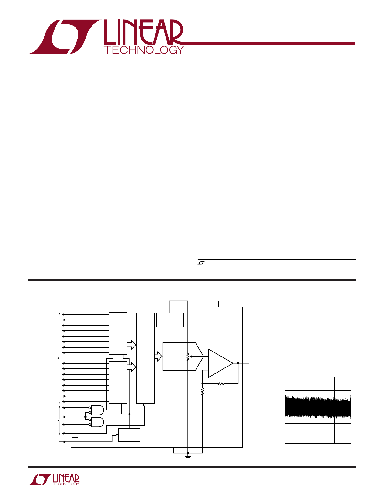
The LTC®1657/LTC1657L are complete single supply, railto-rail voltage output, 16-bit digital-to-analog converters
(DAC) in a 28-pin SSOP or PDIP package. They include a
rail-to-rail output buffer amplifier, an internal reference
and a double buffered parallel digital interface.
The LTC1657/LTC1657L have separate reference input
pins that can be driven by an external reference. The fullscale output can be 1 or 2 times the reference voltage
depending on how the X1/X2 pin is connected. The LTC1657
operates from a 4.5V to 5.5V supply and has an onboard
2.048V reference. The LTC1657L operates from a 2.7V to
5.5V supply and has an onboard 1.25V reference.
The LTC1657/LTC1657L are similar to Linear Technol-
ogy Corporation’s LTC1450/LTC1450L 12-bit V
OUT
DAC
family, allowing an upgrade path. They are the only
buffered 16-bit parallel DACs in a 28-lead SSOP package
and include an onboard reference for stand alone
performance.
, LTC and LT are registered trademarks of Linear Technology Corporation.
BLOCK DIAGRA
D15 (MSB)
19
18
17
16
15
14
13
FROM
12
11
10
28
27
9
8
7
6
5
4
3
1
2
D8
D7
D0 (LSB)
CSMSB
WR
CSLSB
LDAC
CLR
DATA IN FROM
MICROPROCESSOR
DATA BUS
MICROPROCESSOR
DECODE LOGIC
FROM
SYSTEM RESET
W
MSB
8-BIT
INPUT
REGISTER
LSB
8-BIT
INPUT
REGISTER
POWER-ON
RESET
16-BIT
DAC
REGISTER
REFERENCE
LTC1657: 2.048V
LTC1657L: 1.25V
16-BIT
DAC
LTC1657: 4.5V TO 5.5V
LTC1657L: 2.7V TO 5.5V
22 2423
REFHIREFOUT
R
REFLOGND
X1/X2
2120 26
V
CC
+
–
R
V
OUT
1657 TA01
LTC1657:
25
0V TO 4.096V
LTC1657L:
0V TO 2.5V
Differential Nonlinearity
vs Input Code
1.0
0.8
0.6
0.4
0.2
0
–0.2
–0.4
–0.6
DIFFERENTIAL NONLINEARITY (LSB)
–0.8
–1.0
0 16384 32768 49152 65535
DIGITAL INPUT CODE
1657 TA02
1
LTC1657/LTC1657L
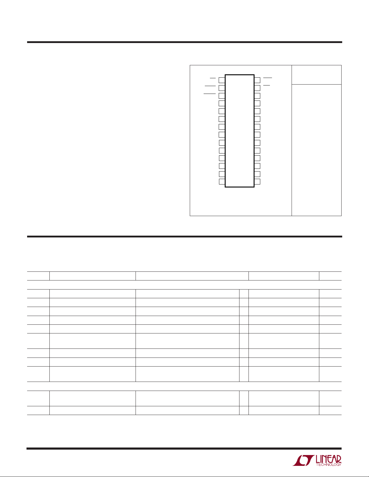
PACKAGE/ORDER I FOR ATIO
UU
W
WWWU
ABSOLUTE AXI U RATI GS
(Note 1)
VCC to GND .............................................. –0.5V to 7.5V
TTL Input Voltage, REFHI, REFLO,
X1/X2....................................................... –0.5V to 7.5V
V
, REFOUT ............................ –0.5V to (VCC + 0.5V)
OUT
Operating Temperature Range
LTC1657C/LTC1657LC .......................... 0°C to 70°C
LTC1657I/LTC1657LI ...................... –40°C to 85°C
Maximum Junction Temperature ..........................125°C
Storage Temperature Range ................ –65°C to 150°C
Lead Temperature (Soldering, 10 sec)................. 300°C
WR
CSLSB
CSMSB
(LSB) D0
D10
TOP VIEW
1
2
3
4
5
D1
6
D2
7
D3
8
D4
9
D5
10
D6
11
D7
12
D8
13
D9
14
28
27
26
25
24
23
22
21
20
19
18
17
16
15
LDAC
CLR
X1/X2
V
OUT
V
CC
REFOUT
REFHI
REFLO
GND
D15 (MSB)
D14
D13
D12
D11
ORDER PART
NUMBER
LTC1657CGN
LTC1657CN
LTC1657IGN
LTC1657IN
LTC1657LCGN
LTC1657LCN
LTC1657LIGN
LTC1657LIN
GN PACKAGE
28-LEAD PLASTIC SSOP
ELECTRICAL CHARACTERISTICS
N PACKAGE
28-LEAD PDIP
T
= 125°C, θJA = 95°C/ W (GN)
JMAX
T
= 125°C, θJA = 58°C/ W (N)
JMAX
Consult factory for parts specified with wider operating temperature ranges.
The ● denotes specifications which apply over the full operating
temperature range, otherwise specifications are at TA = 25°C. VCC = 4.5V to 5.5V (LTC1657), VCC = 2.7V to 5.5V (LTC1657L),
V
unloaded, REFOUT tied to REFHI, REFLO tied to GND, X1/X2 tied to GND, unless otherwise noted.
OUT
SYMBOL PARAMETER CONDITIONS MIN TYP MAX UNITS
DAC (Note 2)
Resolution ● 16 Bits
Monotonicity ● 16 Bits
DNL Differential Nonlinearity Guaranteed Monotonic (Note 3) ● ±0.5 ±1 LSB
INL Integral Nonlinearity (Note 3) ● ±4 ±12 LSB
ZSE Zero Scale Error ● 02mV
V
OS
VOSTC Offset Error Tempco ±5 µV/°C
Power Supply
V
CC
I
CC
Offset Error Measured at Code 200 (LTC1657) ● ±0.3 ±3mV
Measured at Code 200 (LTC1657L)
Gain Error ● ±2 ±16 LSB
Gain Error Drift LTC1657 0.5 ppm/°C
LTC1657L 1.0 ppm/°C
Positive Supply Voltage For Specified Performance (LTC1657) ● 4.5 5.5 V
For Specified Performance (LTC1657L)
Supply Current (Note 4) ● 650 1200 µA
● ±0.4 ±4mV
● 2.7 5.5 V
2
LTC1657/LTC1657L
ELECTRICAL CHARACTERISTICS
The ● denotes specifications which apply over the full operating
temperature range, otherwise specifications are at TA = 25°C. VCC = 4.5V to 5.5V (LTC1657), VCC = 2.7V to 5.5V (LTC1657L),
V
unloaded, REFOUT tied to REFHI, REFLO tied to GND, X1/X2 tied to GND, unless otherwise noted.
OUT
SYMBOL PARAMETER CONDITIONS MIN TYP MAX UNITS
Op Amp DC Performance
Short-Circuit Current Low V
Short-Circuit Current High V
Output Impedance to GND Input Code = 0 (LTC1657) ● 40 120 Ω
Output Line Regulation Input Code = 65535, LTC1657: VCC = 4.5V to 5.5V ● 4 mV/V
AC Performance
Voltage Output Slew Rate (Note 5) ● ±0.3 ±0.7 V/µs
Voltage Output Settling Time (Note 5) to 0.0015% (16-Bit Settling Time) 20 µs
Digital Feedthrough (Note 6) 0.3 nV•s
Midscale Glitch Impulse DAC Switch Between 8000H and 7FFF
Output Voltage Noise Using X1/X2 Tied to V
Internal Reference at 1kHz LTC1657 165 nV/√Hz
Output Voltage Noise Using X1/X2 Tied to V
External Reference at 1kHz
Output Voltage Noise Density Using X1/X2 Tied to V
Internal Reference from 0.1Hz to 10Hz
Refererence Input Multiplying BW 700 kHz
Reference Output (REFOUT)
Reference Output Voltage LTC1657 ● 2.036 2.048 2.060 V
Reference Output 15 ppm/°C
Temperature Coefficient
Reference Line Regulation LTC1657: VCC = 4.5V to 5.5V ● ±1.5 mV/V
Reference Load Regulation Measured at I
Short-Circuit Current REFOUT Shorted to GND ● 50 100 mA
Reference Output Voltage Noise at 1kHz LTC1657 150 nV/√Hz
Reference Output Voltage Noise Density 6 µV
from 0.1Hz to 10Hz
Reference Input
REFHI, REFLO Input Range (Note 7) See Applications Information
REFHI Input Resistance LTC1657 ● 16 25 kΩ
Shorted to GND ● 70 120 mA
OUT
Shorted to V
OUT
Input Code = 0 (LTC1657L)
Input Code = 65535, LTC1657L: V
(Note 5) to 0.012% (13-Bit Settling Time) 10 µs
LTC1657L 105 nV/√Hz
LTC1657L
LTC1657L: V
Measured at I
LTC1657L 90 nV/√Hz
X1/X2 Tied to V
X1/X2 Tied to GND
LTC1657L (Relative to REFLO)
CC
= 2.7V to 5.5V ● 3 mV/V
CC
H
(Notes 8, 9)
OUT
(Notes 8, 9, 10) 50 nV/√Hz
OUT
(Notes 8, 9) 8 µV
OUT
= 2.7V to 5.5V ● ±1.0 mV/V
CC
= 100µA (LTC1657) ● 5 mV/A
OUT
= 100µA (LTC1657L) ● 3 mV/A
OUT
OUT
● 80 140 mA
● 120 275 Ω
8nV•s
P-P
● 1.240 1.250 1.260 V
P-P
● 0V
● 0V
● 16 23 kΩ
– 1.5 V
CC
/2 V
CC
3
LTC1657/LTC1657L
ELECTRICAL CHARACTERISTICS
temperature range TA = T
SYMBOL PARAMETER CONDITIONS MIN TYP MAX MIN TYP MAX UNITS
Digital I/O
V
IH
V
IL
I
LEAK
C
IN
Switching Characteristics
t
CS
t
WR
t
CWS
t
CWH
t
DWS
t
DWH
t
LDAC
t
CLR
Note 1: Absolute Maximum Ratings are those values beyond which the life
of a device may be impaired.
Note 2: External reference REFHI = 2.2V. V
Note 3: Nonlinearity is defined from code 128 to code 65535 (full scale).
See Applications Information.
Note 4: Digital inputs at 0V or V
Note 5: DAC switched between all 1s and all 0s. V
Digital Input High Voltage ● 2.4 2.0 V
Digital Input Low Voltage ● 0.8 0.6 V
Digital Input Leakage VIN = GND to V
Digital Input Capacitance (Note 7) ● 10 10 pF
CS (MSB or LSB) Pulse Width ● 40 60 ns
WR Pulse Width ● 40 60 ns
CS to WR Setup ● 00ns
CS to WR Hold ● 00ns
Data Valid to WR Setup ● 40 60 ns
Data Valid to WR Hold ● 00ns
LDAC Pulse Width ● 40 60 ns
CLR Pulse Width ● 40 60 ns
External reference REFHI = 1.3V. V
MIN
to T
CC
. VCC = 5V (LTC1657), VCC = 3V (LTC1657L), unless otherwise noted.
MAX
= 5V (LTC1657).
CC
= 3V (LTC1657L).
CC
.
= 4.096V.
FS
The ● denotes specifications which apply over the full operating
LTC1657 LTC1657L
CC
● ±10 ±10 µA
Note 6: D0 to D15 toggle between all 0s and all 1s with REFHI = 0V,
CSMSB = CSLSB = WR = LDAC = High
Note 7: Guaranteed by design. Not subject to test.
Note 8: DAC inputs all 1s.
Note 9: X1/X2 tied to GND, the voltage noise will be a factor of 2 greater.
Note 10: Using 2.048V (1.25V) external reference with 3nV/√Hz noise at
1kHz for LTC1657/(LTC1657L).
4
UW
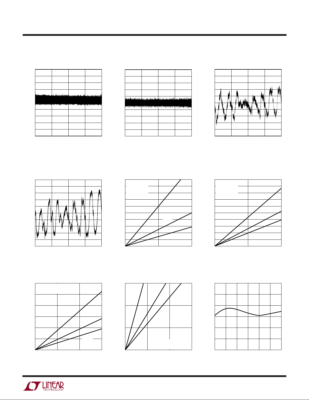
TYPICAL PERFOR A CE CHARACTERISTICS
LTC1657/LTC1657L
LTC1657 Differential Nonlinearity
2.0
1.6
1.2
0.8
0.4
0
–0.4
–0.8
–1.2
DIFFERENTIAL NONLINEARITY (LSB)
–1.6
–2.0
0 16384 32768 49152 65535
5
4
3
2
1
0
–1
–2
–3
INTEGRAL NONLINEARITY (LSB)
–4
–5
0
DIGITAL INPUT CODE
16384
32768
DIGITAL INPUT CODE
49152
1657 G01
65535
1657 G04
LTC1657L Differential Nonlinearity
2.0
1.6
1.2
0.8
0.4
0
–0.4
–0.8
–1.2
DIFFERENTIAL NONLINEARITY (LSB)
–1.6
–2.0
16384
0
32768
DIGITAL INPUT CODE
49152
65535
1657 G02
LTC1657 Minimum Supply
Headroom for Full Output Swing
vs Load CurrentLTC1657L Integral Nonlinearity
2.0
CODE ALL 1s
(V)
OUT
– V
CC
V
1.8
1.6
1.4
1.2
1.0
0.8
0.6
0.4
0.2
≤ 1LSB
∆V
OUT
= 4.096V
V
OUT
125°C
25°C
–55°C
0
0510
LOAD CURRENT (mA)
1657 G05
LTC1657 Integral Nonlinearity
5
4
3
2
1
0
–1
–2
–3
INTEGRAL NONLINEARITY (LSB)
–4
–5
0 16384 32768 49152 65535
DIGITAL INPUT CODE
1657 G03
LTC1657L Minimum Supply
Headroom for Full Output Swing
vs Load Current
2.0
CODE ALL 1s
(V)
OUT
– V
CC
V
1.8
1.6
1.4
1.2
1.0
0.8
0.6
0.4
0.2
0
≤ 1LSB
∆V
OUT
= 2.5V
V
OUT
125°C
25°C
–55°C
0510
LOAD CURRENT (mA)
1657 G06
LTC1657 Minimum Output
Voltage vs Output Sink Current
1.2
CODE ALL 0s
≤ 1LSB
∆V
OUT
1.0
0.8
0.6
0.4
0.2
OUTPUT PULL-DOWN VOLTAGE (V)
0
0
51015
OUTPUT SINK CURRENT (mA)
125°C
25°C
–55°C
1657 G07
LTC1657L Minimum Output
Voltage vs Output Sink Current
0.6
125°C 25°C –55°C
0.4
0.2
OUTPUT PULL-DOWN VOLTAGE (V)
0
0
51015
OUTPUT SINK CURRENT (mA)
CODE ALL 0s
≤ 1LSB
∆V
OUT
1657 G08
LTC1657 Full-Scale Voltage
vs Temperature
4.110
4.105
4.100
4.095
4.090
FULL-SCALE VOLTAGE (V)
4.085
4.080
–55 –25 5 35 65 95 125
TEMPERATURE (°C)
1657 G09
5

LTC1657/LTC1657L
TEMPERATURE (°C)
–55 –35 –15 5 25 45 65 85 105 125
SUPPLY CURRENT (µA)
1657 G15
700
680
660
640
620
600
580
560
540
520
500
VCC = 5.5V
VCC = 5V
VCC = 4.5V
TIME (20µs/DIV)
0
OUTPUT VOLTAGE (V)
2
4
1
3
5
1657 G18
V
OUT
UNLOADED
T
A
= 25°C
UW
TYPICAL PERFOR A CE CHARACTERISTICS
LTC1657L Full-Scale Voltage
vs Temperature
2.510
2.505
2.500
2.495
FULL-SCALE VOLTAGE (V)
2.490
–55
–25 5 35 65
TEMPERATURE (°C)
LTC1657 Supply Current
vs Logic Input Voltage
8
VCC = 5V
7
6
5
4
3
SUPPLY CURRENT (mA)
2
1
0
1 2 3 4 5
0
LOGIC INPUT VOLTAGE (V)
95 125
1657 G10
1657 G13
LTC1657 Offset Error
vs Temperature
1.0
0.9
0.8
0.7
0.6
0.5
0.4
OFFSET (mV)
0.3
0.2
0.1
0
–55
–10 35 80 125
TEMPERATURE (°C)
LTC1657L Supply Current
vs Logic Input Voltage
2.0
VCC = 3V
1.8
1.6
1.4
1.2
1.0
0.8
SUPPLY CURRENT (mA)
0.6
0.4
0.2
0
13
LOGIC INPUT VOLTAGE (V)
LTC1657L Offset Error
vs Temperature
1.0
0.8
0.6
0.4
0.2
0
–0.2
OFFSET (mV)
–0.4
–0.6
– 0.8
1657 G11
–1.0
–55
–10 35 80 125
TEMPERATURE (°C)
1657 G12
LTC1657 Supply Current
vs Temperature
2
1657 G14
LTC1657L Supply Current
vs Temperature
560
550
540
530
520
6
510
SUPPLY CURRENT (µA)
VCC = 3V
500
490
480
470
460
–55 –35 –15 5 25 45 65 85 105 125
VCC = 3.3V
TEMPERATURE (°C)
VCC = 2.7V
1657 G16
LTC1657
Large-Signal Transient Response
5
V
UNLOADED
OUT
T
= 25°C
A
4
3
2
OUTPUT VOLTAGE (V)
1
0
TIME (20µs/DIV)
LTC1657L
Large-Signal Transient Response
1657 G17

UW
TYPICAL PERFOR A CE CHARACTERISTICS
LTC1657/LTC1657L
LTC1657 0.1Hz to 10Hz
Voltage Noise
1µV/DIV
8
1659 G19
U
246 107135 9
0
TIME (SEC)
UU
PI FU CTIO S
WR (Pin 1): Write Input (Active Low). Used with CSMSB
and/or CSLSB to control the input registers. While WR and
CSMSB and/or CSLSB are held low, data writes into the
input register.
CSLSB (Pin 2): Chip Select Least Significant Byte (Active
Low). Used with WR to control the LSB 8-bit input registers. While WR and CSLSB are held low, the LSB byte
writes into the LSB input register. Can be connected to
CSMSB for simultaneous loading of both sets of input
latches on a 16-bit bus.
CSMSB (Pin 3): Chip Select Most Significant Byte (Active
Low). Used with WR to control the MSB 8-bit input
registers. While WR and CSMSB are held low, the MSB
byte writes into the MSB input register. Can be connected
to CSLSB for simultaneous loading of both sets of input
latches on a 16-bit bus.
D0 to D7 (Pins 4 to 11): Input data for the Least Significant
Byte. Written into LSB input register when WR = 0 and
CSLSB = 0.
D8 to D15 (Pins 12 to 19): Input data for the Most Significant Byte. Written into MSB input register when WR = 0
and CSMSB = 0.
LTC1657L 0.1Hz to 10Hz
Voltage Noise
1µV/DIV
246 107135 9
0
TIME (SEC)
8
1659 G20
REFLO (Pin 21): Lower input terminal of the DAC’s internal resistor ladder. Typically connected to Analog Ground.
An input code of (0000)H will connect the positive input of
the output buffer to this end of the ladder. Can be used to
offset the zero scale above ground.
REFHI (Pin 22): Upper input terminal of the DAC’s internal
resistor ladder. Typically connected to REFOUT. An input
code of (FFFF)H will connect the positive input of the
output buffer to 1LSB below this voltage.
REFOUT (Pin 23): Output of the internal reference is
2.048V (LTC1657), 1.25V (LTC1657L). Typically connected to REFHI to drive internal DAC resistor ladder.
VCC (Pin 24): Positive Power Supply Input. 4.5V ≤ VCC ≤
5.5V (LTC1657), 2.7V ≤ VCC ≤ 5.5V (LTC1657L). Requires
a 0.1µF bypass capacitor to ground.
V
(Pin 25): Buffered DAC Output.
OUT
X1/X2 (Pin 26): Gain Setting Resistor Pin. Connect to GND
for G = 2 or to V
tied to a low impedance source, such as ground or V
for G = 1. This pin should always be
OUT
OUT
,
to ensure stability of the output buffer when driving
capacitive loads.
GND (Pin 20): Ground.
7

LTC1657/LTC1657L
U
UU
PI FU CTIO S
CLR (Pin 27): Clear Input (Asynchronous Active Low). A
low on this pin asynchronously resets all input and DAC
registers to 0s.
U
DIGITAL INTERFACE TRUTH TABLE
CLR CSMSB CSLSB WR LDAC FUNCTION
L X X X X Clears input and DAC registers to zero
H X X X L Loads DAC register with contents of input registers
H X X X H Freezes contents of DAC register
H L H L X Writes MSB byte into MSB input register
H H L L X Writes LSB byte into LSB input register
H L L L X Writes MSB and LSB bytes into MSB and LSB input registers
H X X H X Inhibits write to MSB and LSB input registers
H H X X X Inhibits write to MSB input register
H X H X X Inhibits write to LSB input register
H L L L L Data bus flows directly through input and DAC registers
LDAC (Pin 28): Load DAC (Asynchronous Active Low).
Used to asynchronously transfer the contents of the input
registers to the DAC register which updates the output
voltage. If held low, the DAC register loads data from the
input registers which will immediately update V
OUT
.
WUW
TIMING DIAGRAM
CSLSB
CSMSB
WR
LDAC
DATA
t
CWS
t
CS
t
CS
t
t
WR
t
CWH
t
DWH
DWS
DATA VALID DATA VALID
t
WR
t
LDAC
DAC UPDATE
1657 TD
8

UU
DEFI ITIO S
LTC1657/LTC1657L
Resolution (n): Resolution is defined as the number of
digital input bits (n). It defines the number of DAC output
states (2n) that divide the full-scale range. Resolution does
not imply linearity.
Full-Scale Voltage (VFS): This is the output of the DAC
when all bits are set to 1.
Voltage Offset Error (VOS): Normally, the DAC offset is the
voltage at the output when the DAC is loaded with all zeros.
The DAC can have a true negative offset, but because the
part is operated from a single supply, the output cannot go
below zero. If the offset is negative, the output will remain
near 0V resulting in the transfer curve shown in Figure 1.
OUTPUT
VOLTAGE
NEGATIVE
OFFSET
0V
Figure 1. Effect of Negative Offset
DAC CODE
1657 F01
The offset of the part is measured at the code that corresponds to the maximum offset specification:
VOS = V
– [(Code)(VFS)/(2n – 1)]
OUT
Least Significant Bit (LSB): One LSB is the ideal voltage
difference between two successive codes.
LSB = G • V
G = 1 for X1/X2 connected to V
REF
/65536
OUT
G = 2 for X1/X2 connected to GND
Nominal LSBs: (V
REFOUT
tie to V
, REFLO tie to GND,
REFHI
G = 2)
LTC1657 LSB = 4.096V/65536 = 62.5µV
LTC1657L LSB = 2.5V/65536 = 38.1µV
DAC Transfer Characteristic:
VG
OUT
REFHI REFLO
=
–
65536
G = 1 for X1/X2 connected to V
CODE REFLO
()
OUT
+•
G = 2 for X1/X2 connected to GND
CODE = Decimal equivalent of digital input
(0 ≤ CODE ≤ 65535)
Zero-Scale Error (ZSE): The output voltage when the
DAC is loaded with all zeros. Since this is a single supply
part, this value cannot be less than 0V.
Integral Nonlinearity (INL): End-point INL is the maximum deviation from a straight line passing through the
end points of the DAC transfer curve. Because the part
operates from a single supply and the output cannot go
below zero, the linearity is measured between full scale
and the code corresponding to the maximum offset
specification. The INL error at a given input code is
calculated as follows:
INL (In LSBs) = [V
– VOS – (VFS – VOS)
OUT
(code/65535)]
V
= The output voltage of the DAC measured at
OUT
the given input code
Differential Nonlinearity (DNL): DNL is the difference
between the measured change and the ideal one LSB
change between any two adjacent codes. The DNL error
between any two codes is calculated as follows:
DNL = (∆V
∆V
OUT
= The measured voltage difference between
– LSB)/LSB
OUT
two adjacent codes
Digital Feedthrough: The glitch that appears at the analog
output caused by AC coupling from the digital inputs when
they change state. The area of the glitch is specified in
nV • s.
9

LTC1657/LTC1657L
U
OPERATIO
Parallel Interface
The data on the input of the DAC is written into the DAC’s
input registers when Chip Select (CSLSB and/or CSMSB)
and WR are at a logic low. The data that is written into the
input registers will depend on which of the Chip Selects
are at a logic low (see Digital Interface Truth Table). If WR
and CSLSB are both low and CSMSB is high, then only
data on the eight LSBs (D0 to D7) is written into the input
registers. Similarly, if WR and CSMSB are both low and
CSLSB is high, then only data on the eight MSBs (D8 to
D15) is written into the input registers. Data is written into
both the Least Significant Data Bits (D0 to D7) and the Most
Significant Bits (D8 to D15) at the same time if WR, CSLSB
and CSMSB are low. If WR is high or both CSMSB and
CSLSB are high, then no data is written into the input
registers.
Once data is written into the input registers, it can be
written into the DAC register. This will update the analog
voltage output of the DAC. The DAC register is written by
a logic low on LDAC. The data in the DAC register will be
held when LDAC is high.
When WR, CSLSB, CSMSB and LDAC are all low, the
registers are transparent and data on pins D0 to D15 flows
directly into the DAC register.
For an 8-bit data bus connection, tie the MSB byte data
pins to their corresponding LSB byte pins (D15 to D7, D14
to D6, etc).
Power-On Reset
resistor ladder, an external reference can be used or the
resistor ladder can be driven by an external source in
multiplying applications. The external reference or source
must be capable of driving the 16k (minimum) DAC ladder
resistance.
Internal reference output noise can be reduced with a
bypass capacitor to ground. (Note: The reference does not
require a bypass capacitor to ground for nominal operation.) When bypassing the reference, a small value resistor in series with the capacitor is recommended to help
reduce peaking on the output. A 10Ω resistor in series
with a 4.7µF capacitor is optimum for reducing reference
generated noise. Internal reference output voltage noise
spectral density at 1kHz is typically 150nV/√Hz (LTC1657),
90nV/√Hz (LTC1657L)
DAC Resistor Ladder
The high and low end of the DAC ladder resistor string
(REFHI and REFLO, respectively) are not connected internally on this part. Typically, REFHI will be connected to
REFOUT and REFLO will be connected to GND. X1/X2
connected to GND will give the
scale output swing of 4.096V/2.5V.
Either of these pins can be driven up to VCC – 1.5V when
using the buffer in the gain-of-1 configuration. The resistor
string pins can be driven to VCC/2 when the buffer is in the
gain of 2 configuration. The resistance between these two
pins is typically 25k (16k min) (LTC1657), 23k (16k min)
(LTC1657L).
LTC1657/LTC1657L
a full-
The LTC1657/LTC1657L have an internal power-on reset
that resets all internal registers to 0’s on power-up and
V
pin forces to GND (equivalent to the CLR pin
OUT
function).
Reference
The
LTC1657/LTC1657L
reference, giving the
of 4.096V/2.5V in the gain-of-2 configuration. The onboard
reference in the
connected to the DAC’s reference resistor string but is
provided on an adjacent pin for flexibility. Because the
internal reference is not internally connected to the DAC
include an internal 2.048V/1.25V
LTC1657/LTC1657L
LTC1657/LTC1657L
a full-scale range
is not internally
10
Voltage Output
The output buffer for the LTC1657/LTC1657L can be
configured for two different gain settings. By tying the
X1/X2 pin to GND, the gain is set to 2. By tying the X1/X2
pin to V
The
LTC1657/LTC1657L
source or sink 5mA within 500mV of the positive supply
voltage or ground at room temperature. The output stage
is equipped with a deglitcher that results in a midscale
glitch impulse of 8nV • s. The output swings to within a few
millivolts of either supply rail when unloaded and has an
equivalent output resistance of 40Ω (LTC1657), 120Ω
(LTC1657L) when driving a load to the rails.
, the gain is set to unity.
OUT
rail-to-rail buffered output can

WUUU
APPLICATIO S I FOR ATIO
LTC1657/LTC1657L
Rail-to-Rail Output Considerations
In any rail-to-rail DAC, the output swing is limited to
voltages within the supply range.
If the DAC offset is negative, the output for the lowest
codes limits at 0V as shown in Figure 1b.
V
CC
Similarly, limiting can occur near full scale when the REF
pin is tied to VCC/2. If V
= VCC/2 and the DAC full-scale
REF
error (FSE) is positive, the output for the highest codes
limits at VCC as shown in Figure 1c. No full-scale limiting
can occur if V
is less than (VCC – FSE)/2.
REF
Offset and linearity are defined and tested over the region
of the DAC transfer function where no output limiting can
occur.
POSITIVE
FSE
V
CC
V
INPUT CODE
(c)
REF
= VCC/2
OUTPUT
VOLTAGE
= VCC/2
V
REF
327680 65535
INPUT CODE
(a)
OUTPUT
VOLTAGE
NEGATIVE
OFFSET
OUTPUT
VOLTAGE
0V
INPUT CODE
(b)
Figure 2. Effects of Rail-to-Rail Operation On a DAC Transfer Curve. (a) Overall Transfer Function (b) Effect of Negative
Offset for Codes Near Zero Scale (c) Effect of Positive Full-Scale Error for Input Codes Near Full Scale When V
= VCC/2
REF
1657 F02
11

LTC1657/LTC1657L
TYPICAL APPLICATIO S
U
This circuit shows how to make a bipolar output 16-bit
DAC with a wide output swing using an LTC1657 and an
LT1077. R1 and R2 resistively divide down the LTC1657
output and an offset is summed in using the LTC1657
onboard 2.048V reference and R3 and R4. R5 ensures that
A Wide Swing, Bipolar Output 16-Bit DAC
5V
0.1µF
R5
100k
1%
24
V
CC
V
OUT
R3
100k
1%
5:19
DATA (0:15)
2
CSLSB
3
µP
CSMSB
1
WR
28
LDAC
27
CLR
26 21 20 22 23
LTC1657
GND REFHI REFOUTREFLOX1/X2
the onboard reference is always sourcing current and
never has to sink any current even when V
is at full
OUT
scale. The LT1077 output will have a wide bipolar output
swing of – 4.096V to 4.096V as shown in the figure below.
With this output swing, 1LSB = 125µV.
25
R1
100k
1%
R2
200k
1%
5V
3
2
+
LT1077
–
–5V
7
6
4
R4
200k
1%
(2)(DIN)(4.096)
V
: – 4.096V
OUT
65536
1657 TA05
12
4.096
V
OUT
–4.096
0
TRANSFER CURVE
32768
65535
D
IN

TYPICAL APPLICATIO S
LTC1657/LTC1657L
U
This circuit shows a digitally programmable current source
from an external voltage source using an external op amp,
an LT1218 and an NPN transistor (2N3440). Any digital
word from 0 to 65535 is loaded into the LTC1657 and its
output correspondingly swings from 0V to 4.096V. This
voltage will be forced across the resistor RA. If RA is
Digitally Programmable Current Source
5V
5:19
DATA (0:15)
2
CSLSB
3
µP
CSMSB
1
WR
28
LDAC
27
CLR
22 23
REFOUTREFHI
LTC1657
GND
REFLOX1/X2
26 21 20
V
CC
V
OUT
chosen to be 412Ω, the output current will range from
0mA at zero scale to 10mA at full scale. The minimum
voltage for VS is determined by the load resistor RL and
Q1’s V
voltage. With a load resistor of 50Ω, the
CESAT
voltage source can be 5V.
5V < VS < 100V
≤ 50Ω
FOR R
L
R
7
4
L
6
Q1
2N3440
R
A
412Ω
1%
(DIN)(4.096)
I
=
OUT
(65536)(R
≈ 0mA TO 10mA
1657 TA04
)
A
25 3
0.1µF
2
+
LT1218
–
13

LTC1657/LTC1657L
PACKAGE DESCRIPTIO
U
Dimensions in inches (millimeters) unless otherwise noted.
GN Package
28-Lead Plastic SSOP (Narrow 0.150)
(LTC DWG # 05-08-1641)
0.015
± 0.004
(0.38 ± 0.10)
0.0075 – 0.0098
(0.191 – 0.249)
0.016 – 0.050
(0.406 – 1.270)
* DIMENSION DOES NOT INCLUDE MOLD FLASH. MOLD FLASH
SHALL NOT EXCEED 0.006" (0.152mm) PER SIDE
** DIMENSION DOES NOT INCLUDE INTERLEAD FLASH. INTERLEAD
FLASH SHALL NOT EXCEED 0.010" (0.254mm) PER SIDE
0° – 8° TYP
× 45°
0.229 – 0.244
(5.817 – 6.198)
0.053 – 0.069
(1.351 – 1.748)
0.008 – 0.012
(0.203 – 0.305)
12
3
0.386 – 0.393*
(9.804 – 9.982)
5
4
678 9 10 11 12
0.0250
(0.635)
BSC
0.033
202122232425262728
19
18
16
17
13 14
(0.838)
15
(0.102 – 0.249)
REF
0.150 – 0.157**
(3.810 – 3.988)
0.004 – 0.009
GN28 (SSOP) 1098
14

PACKAGE DESCRIPTIO
U
Dimensions in inches (millimeters) unless otherwise noted.
N Package
28-Lead PDIP (Narrow 0.300)
(LTC DWG # 05-08-1510)
1.370*
(34.789)
MAX
23
2425
22
0.255 ± 0.015*
(6.477 ± 0.381)
26
27
28
LTC1657/LTC1657L
171920
151618
2
1
0.300 – 0.325
(7.620 – 8.255)
0.009 – 0.015
(0.229 – 0.381)
+0.035
0.325
–0.015
+0.889
8.255
()
–0.381
*THESE DIMENSIONS DO NOT INCLUDE MOLD FLASH OR PROTRUSIONS.
MOLD FLASH OR PROTRUSIONS SHALL NOT EXCEED 0.010 INCH (0.254mm)
(3.302 ± 0.127)
0.020
(0.508)
MIN
0.125
(3.175)
MIN
0.130 ± 0.005
0.005
(0.127)
MIN
3456
0.045 – 0.065
(1.143 – 1.651)
0.100
(2.54)
BSC
7
9
8
10 11 122113 14
0.065
(1.651)
TYP
0.018 ± 0.003
(0.457 ± 0.076)
N28 1098
Information furnished by Linear Technology Corporation is believed to be accurate and reliable.
However, no responsibility is assumed for its use. Linear Technology Corporation makes no representation that the interconnection of its circuits as described herein will not infringe on existing patent rights.
15

LTC1657/LTC1657L
TYPICAL APPLICATIO S
U
This circuit shows how to measure negative offset. Since
LTC1657/LTC1657L operate on a single supply, if their
offset is negative, the output for code 0 limits at 0V. To
Negative Offset Measurement
5:19
DATA (0:15)
2
CSLSB
3
µP
CSMSB
1
WR
28
LDAC
27
CLR
LTC1657/LTC1657L
REFLOX1/X2
26 21 20
Although LTC1657 output is up to 4.096V with its internal
reference, higher voltages can be achieved with the help of
another op amp. The following circuit shows how to
increase the output swing of LTC1657 by using an LT1218.
A Higher Voltage Output DAC
5V
measure this negative offset, a negative supply is needed,
connect resistor R1 as shown in the figure. The output
voltage is the offset when code 0 is loaded in.
5V
22 23 24
V
REFOUTREFHI
CC
GND
V
OUT
0.1µF
25
R1
100k
–5V
1657 TA06
As shown in the configuration, the output of LTC1657 is
amplified by 8 for an output swing of 0V to 32.768V, or a
convenient 0.5mV/LSB.
5:19
DATA (0:15)
2
CSLSB
3
µP
CSMSB
1
WR
28
LDAC
27
CLR
22 23 24
REFOUTREFHI
LTC1657
GND
REFLOX1/X2
26 21 20
V
CC
V
OUT
0.1
325
2
R1
1k
1%
µF
+
LT1218
–
36V
0.1µF
7
6
(DIN)(4.096)
V
=1 +
4
R2
6.98k
1%
OUT
65536
RELATED PARTS
PART NUMBER DESCRIPTION COMMENTS
LTC1446(L) Dual 12-Bit V
LTC1450(L) Single 12-Bit V
LTC1458(L) Quad 12-Bit Rail-to-Rail Output DACs with Added Functionality VCC = 5V (3V), V
LTC1650 Single 16-Bit V
LTC1654 Dual 14-Bit V
LTC1655(L) Single 16-Bit V
LTC1658 Single 14-Bit V
DACs in SO-8 Package VCC = 5V (3V), V
OUT
DACs with Parallel Interface VCC = 5V (3V), V
OUT
Industrial DAC in 16-Pin SO VCC = ±5V, Low Power, Deglitched, 4-Quadrant Multiplying V
OUT
DAC Programmable Speed/Power, SO-8 Footprint
OUT
DAC with Serial Interface in SO-8 VCC = 5V (3V), Low Power, Deglitched, V
OUT
(0V to 2.5V)
DAC in MSOP Package 2.7V to 5.5V Operation, Low Power
OUT
OUT
0
TRANSFER CURVE
D
IN
= 0V to 4.096V
OUT
65535
1657 TA07
32.768 (V)
V
R2
R1
()
= 0V to 4.095V (0V to 2.5V)
OUT
= 0V to 4.095V (0V to 2.5V)
OUT
= 0V to 4.095V (0V to 2.5V)
OUT
OUT
16
Linear Technology Corporation
1630 McCarthy Blvd., Milpitas, CA 95035-7417
(408) 432-1900 ● FAX: (408) 434-0507
●
www.linear-tech.com
1657lf LT/TP 0201 4K • PRINTED IN USA
LINEAR TECHNOLOGY CORPORATION 1999
 Loading...