

Linear Technology LTC1535 Datasheet
Final Electrical Specifications
FEATURES
LTC1535
Isolated RS485 Transceiver
August 1999
U
DESCRIPTIO
■
UL Rated Isolated RS485: 2500V
■
Half- or Full-Duplex
■
Eliminates Ground Loops
■
350kBd Maximum Data Rate
■
Self-Powered with 400kHz Converter
■
Fail-Safe Output High for Open or
RMS
Shorted Receiver Inputs
■
Short-Circuit Current Limit
■
Slow Slew Rate Control
■
68kΩ Input Impedance Allows Up to 128 Nodes
■
Thermal Shutdown
■
8kV ESD Protection On Driver Outputs and Receiver
Inputs
U
APPLICATIO S
■
Isolated RS485 Receiver/Driver
■
RS485 with Large Common Mode Voltage
■
Breaking RS485 Ground Loops
■
Multiple Unterminated Line Taps
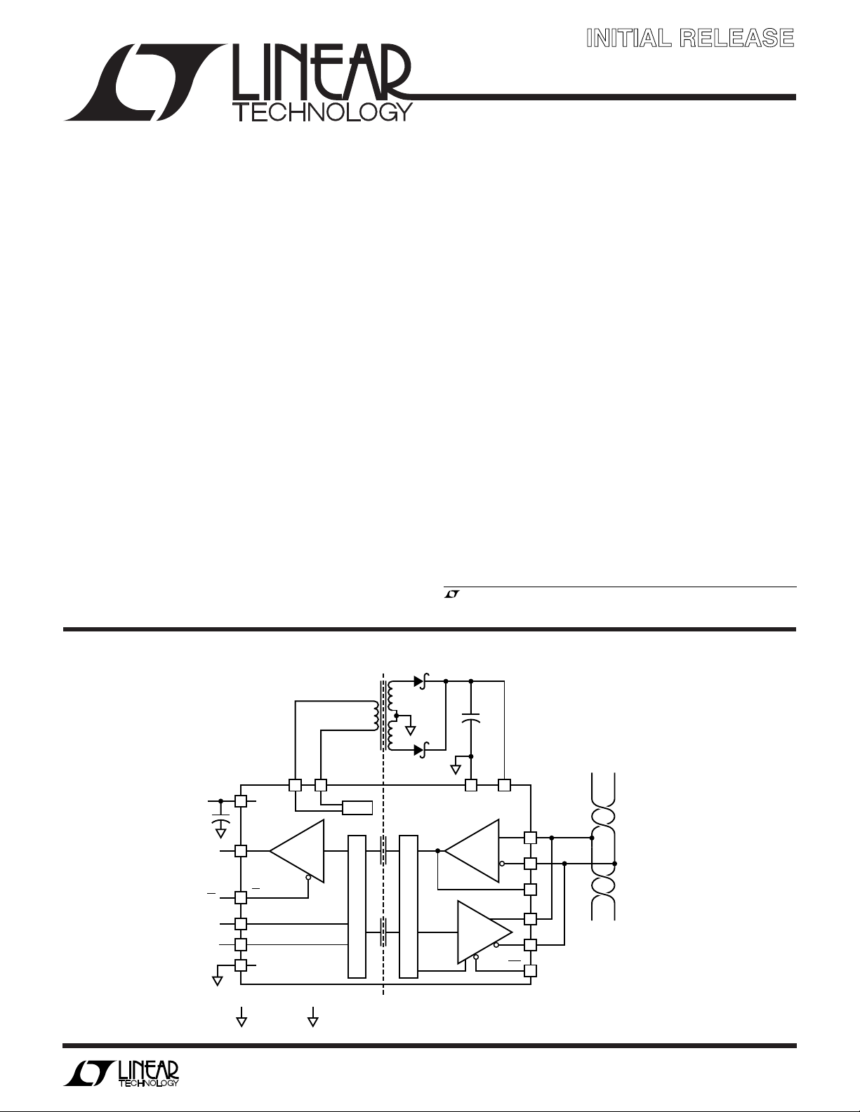
The LTC®1535 is an isolated RS485 full-duplex differential
line transceiver. Isolated RS485 is ideal for systems where
the ground loop is broken to allow for much larger common mode voltage ranges. An internal capacitive isolation
barrier provides 2500V
of isolation between the line
RMS
transceiver and the logic level interface. The powered side
contains a 400kHz push-pull converter to power the isolated RS485 transceiver. Internal full-duplex communication occurs through the capacitive isolation barrier. The
transceiver meets RS485 and RS422 requirements.
The driver and receiver feature three-state outputs, with
the driver maintaining high impedance over the entire
common mode range. The drivers have short-circuit current limits in both directions and a slow slew rate select to
minimize EMI or reflections. The 68kΩ receiver input
allows up to 128 node connections. A fail-safe feature
defaults to a high output state when the receiver inputs are
open or shorted.
, LTC and LT are registered trademarks of Linear Technology Corporation.
TYPICAL APPLICATIO
1
1
28
27
26
25
4
1
V
RO
RE
DE
DI
GND
LOGIC COMMON
1
V
CC
10µF
+
RO
RE
DE
DI
U
ST1 ST2
CC
**
CTX02-14659
32
400kHz
FLOATING RS485 COMMON ** TRANSFORMER
2
1/2 BAT54C
2
1/2 BAT54C
2
COILTRONICS (561) 241-7876
+
GND2
10µF
1411
V
CC2
A
R
D
B
RO2
Y
Z
SLO
1535 TA01
16
15
17
13
12
18
TWISTED-PAIR
CABLE
Information furnished by Linear Technology Corporation is believed to be accurate and reliable.
However, no responsibility is assumed for its use. Linear Technology Corporation makes no representation that the interconnection of its circuits as described herein will not infringe on existing patent rights.
1
LTC1535
WW
W
U
ABSOLUTE AXI U RATI GS
(Note 1)
VCC to GND ................................................................ 6V
V
to GND2 ............................................................ 8V
CC2
Control Input Voltage to GND ...... –0.3V to (VCC + 0.3V)
Driver Input Voltage to GND ........ –0.3V to (VCC + 0.3V)
Driver Output Voltage
(Driver Disabled) to GND2 ..............(V
Driver Output Voltage
(Driver Enabled) to GND2 ............... (V
Receiver Input Voltage to GND2 ............................ ±14V
Receiver Output Voltage .............. –0.3V to (VCC + 0.3V)
Operating Temperature Range ..............0°C ≤ TA ≤ 70°C
Lead Temperature (Soldering, 10 sec)..................300°C
– 13V) to 13V
CC2
– 13V) to 10V
CC2
UUW
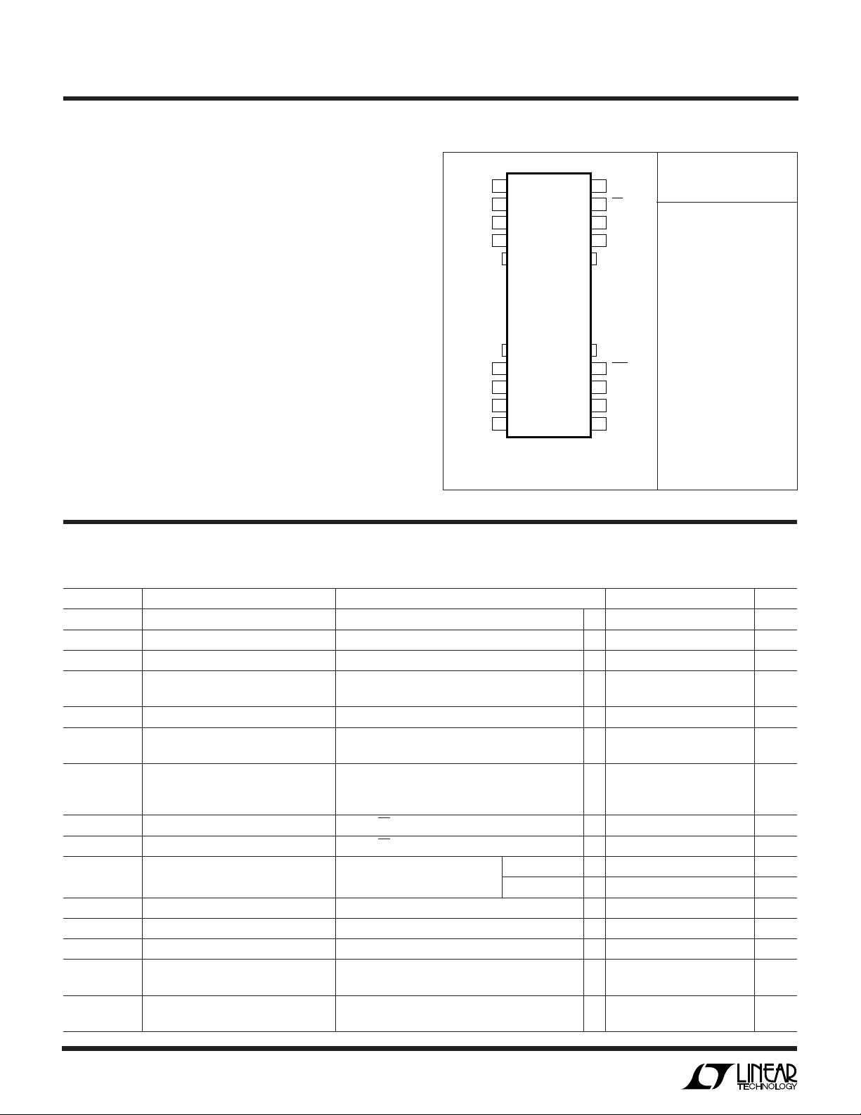
PACKAGE/ORDER I FOR ATIO
TOP VIEW
1
V
CC
2
ST1
3
ST2
4
GND
11
GND2
12
Z
13
Y
14
V
CC2
SW PACKAGE
28-LEAD PLASTIC SO WIDE
T
= 125°C, θJA = 125°C/W
JMAX
Consult factory for Industrial and Military grade parts.
28
RO
27
RE
26
DE
25
DI
18
SLO
17
RO2
16
A
15
B
ORDER PART
NUMBER
LTC1535CSW
ELECTRICAL CHARACTERISTICS
temperature range, otherwise specifications are at T
SYMBOL PARAMETER CONDITIONS MIN TYP MAX UNITS
V
CC
V
CC2
I
CC
I
CC2
V
OD1
V
OD2
I
OSD1
V
IH
V
IL
I
IN
V
TH
∆V
R
IN
V
OH
V
OL
TH
VCC Supply Range ● 4.5 5.5 V
V
Supply Range ● 4.5 7.5 V
CC2
VCC Supply Current No Load ● 13 18 mA
V
Supply Current R = 27Ω, Figure 1 ● 63 73 mA
CC2
Differential Driver Output No Load ● 5V
Differential Driver Output R = 50Ω (RS422) Note 2 ● 2V
Driver Short-Circuit Current
= HIGH –7V ≤ VCM ≤ 10V ● 75 100 135 mA
V
OUT
V
= LOW –7V ≤ VCM ≤ 10V ● 75 100 135 mA
OUT
Logic Input High Voltage DE, DI, RE VCC = 4.5V ● 2V
Logic Input Low Voltage DE, DI, RE VCC = 4.5V ● 0.8 V
Input Current (A, B) Note 3 VIN = 12V ● 0.25 mA
Receiver Input Threshold –7V ≤ VCM ≤ 12V, Note 4 ● –200 –90 –10 mV
Receiver Input Hysteresis –7V ≤ VCM ≤ 12V ● 10 30 70 mV
Receiver Input Impedance ● 50 68 85 kΩ
RO Output High Voltage IRO = –4mA, VCC = 4.5V ● 3.7 4.0 V
RO Output Low Voltage IRO = 4mA, VCC = 4.5V ● 0.4 0.8 V
No Load
R = 27Ω(RS485), Figure 1
I
I
The ● denotes the specifications which apply over the full operating
= 25°C. 0°C ≤ TA ≤ 70°C, V
A
= –10mA, VCC = 4.5V 3.4 V
RO
= 10mA, VCC = 4.5V 0.9 V
RO
= 5V, V
CC
VIN = –7V ● –0.20 mA
= 5V unless otherwise noted.
CC2
● 712 mA
● 1.5 2 V
2
LTC1535
ELECTRICAL CHARACTERISTICS
temperature range, otherwise specifications are at T
The ● denotes the specifications which apply over the full operating
= 25°C. 0°C ≤ TA ≤ 70°C, V
A
= 5V, V
CC
= 5V unless otherwise noted.
CC2
SYMBOL PARAMETER CONDITIONS MIN TYP MAX UNITS
I
V
V
f
R
R
I
I
V
V
V
OZ
OH2
OL2
SW
SWH
SWL
REL
REH
UVL
UVH
ISO
Driver Output Leakage 1 µA
RO2 Output High Voltage I
RO2 Output Low Voltage I
= –4mA, VCC = 4.5V ● 3.7 3.9 V
RO2
I
= –10mA, VCC = 4.5V 3.4 V
RO2
= 4mA, VCC = 4.5V ● 0.4 0.8 V
RO2
I
= 10mA, VCC = 4.5V 0.9 V
RO2
DC Converter Frequency ● 290 420 520 kHz
DC Converter R High VCC = 4.5V ● 46 Ω
DC Converter R Low VCC = 4.5V ● 2.5 5 Ω
RE Output Low Current RE Sink Current, Fault = 0 ● –40 –50 –80 µA
RE Output High Current RE Source Current, Fault = 1 ● 80 100 130 µA
Undervoltage Low Threshold RE Fault = 1, Note 5 ● 3.90 4.00 4.25 V
Undervoltage High Threshold RE Fault = 0, Note 5 ● 4.05 4.20 4.40 V
Isolation Voltage 1 Minute, Note 6 2500 V
1 Second 3000 V
RMS
RMS
U
SWITCHI G CHARACTERISTICS
temperature range, otherwise specifications are at T
otherwise noted.
The ● denotes the specifications which apply over the full operating
= 25°C. 0°C ≤ TA ≤ 70°C, V
A
= 5V, V
CC
= 5V, R = 27Ω (RS485) unless
CC2
SYMBOL PARAMETER CONDITIONS MIN TYP MAX UNITS
t
SJ
f
MAX
t
PLH
t
PHL
tr, t
t
ZH
t
ZL
t
LZ
t
HZ
t
PLH
t
PHL
t
PLH
t
PHL
tr, t
t
LZ
t
HZ
t
START
t
TOF
f
f
Data Sample Jitter Figure 8, Note 7 ● 250 285 ns
Max Baud Rate Jitter = 10% Max, SLO = 1, Note 8 ● 350 kBd
Driver Input to Output DE = 1, SLO = 1, Figure 3, Figure 5 ● 600 855 ns
DE = 1, SLO = 0, Figure 3, Figure 5
● 1300 1560 ns
Driver Input to Output DE = 1, SLO = 1, Figure 3, Figure 5 ● 600 855 ns
DE = 1, SLO = 0, Figure 3, Figure 5
● 1300 1560 ns
Driver Rise or Fall Time DE = 1, SLO = 1, Figure 3, Figure 5 ● 20 50 ns
DE = 1, SLO = 0
● 150 500 1000 ns
Driver Enable to Output DI = 1, SLO = 1, Figure 4, Figure 6 ● 1000 1400 ns
Driver Enable to Output DI = 0, SLO = 1, Figure 4, Figure 6 ● 1000 1400 ns
Driver Disable to Output DI = 0, SLO = 1, Figure 4, Figure 6 ● 700 1000 ns
Driver Disable to Output DI = 1, SLO = 1, Figure 4, Figure 6 ● 700 1000 ns
Receiver Input to RO RE = 0, Figure 2, Figure 7 ● 600 855 ns
Receiver Input to RO RE = 0, Figure 2, Figure 7 ● 600 855 ns
Receiver Input to RO2 RE = 0, Figure 2, Figure 7 30 ns
Receiver Input to RO2 RE = 0, Figure 2, Figure 7 30 ns
Receiver Rise or Fall Time RE = 0, Figure 2, Figure 7 20 ns
Receiver Disable to Output Figure 2, Figure 8 30 ns
Receiver Disable to Output Figure 2, Figure 8 30 ns
Initial Start-Up Time Note 9 1200 ns
Data Time-Out Fault Note 9 1200 ns
3

LTC1535
ELECTRICAL CHARACTERISTICS
Note 1: Absolute Maximum Ratings are those values beyond which the
life of a device may be impaired.
Note 2: RS422 50Ω specification based on RS485 27Ω test.
Note 3: IIN is tested at V
V
= GND2 ≤ 5.25V.
CC2
Note 4: Input fault conditions on the RS485 receiver are detected with a
fixed receiver offset. The offset is such that an input short or open will
result in a high data output.
Note 5: The low voltage detect faults when V
and reenables when greater than 4.4V. The fault can be monitored
through the weak driver output on RE.
Note 6: Value derived from 1 second test.
= 5V, guaranteed by design from
CC2
or VCC drops below 4.2V
CC2
UUU
PI FU CTIO S
POWER SIDE
V
(Pin 1): 5V Supply. Bypass to GND with 10µF capaci-
CC
tor.
ST1 (Pin 2): DC Converter Output 1 to DC Transformer.
ST2 (Pin 3): DC Converter Output 2 to DC Transformer.
GND (Pin 4): Ground.
Note 7: The input signals are internally sampled and encoded. The internal
sample rate determines the data output jitter since the internal sampling is
asynchronous with respect to the external data. Nominally, a 4MHz
internal sample rate gives 250ns of sampling uncertainty in the input
signals.
Note 8: The maximum baud rate is 350kBd with 10% sampling jitter.
Lower baud rates have lower jitter.
Note 9: Start-up time is the time for communication to recover after a fault
condition. Data time-out is the time a fault is indicated on RE after data
communication has stopped.
ISOLATED SIDE
GND2 (Pin 11): Isolated Side Power Ground.
Z (Pin 12): Differential Driver Inverting Output.
Y (Pin 13): Differential Driver Noninverting Output.
V
(Pin 14): 5V to 7.5V Supply from DC Transformer.
CC2
Bypass to GND with 10µF capacitor.
DI (Pin 25): Transmit Data TTL Input to the Isolated Side
RS485 Driver. Do not float.
DE (Pin 26): Transmit Enable TTL Input to the Isolated
Side RS485 Driver. A high level enables the driver. Do not
float.
RE (Pin 27): Receive Data Output Enable TTL Input. A low
level enables the receiver. This pin also provides a fault
output signal. (See Applications Information.)
RO (Pin 28): Receive Data TTL Output.
B (Pin 15): Differential Receiver Inverting Input.
A (Pin 16): Differential Receiver Noninverting Input.
RO2 (Pin 17): Isolated Side Receiver TTL Output.
SLO (Pin 18): Slow Slew Rate Control of RS485 Driver. A
low level forces the driver outputs into slow slew rate
mode.
4
 Loading...